ISSN(Online): 2319-8753 ISSN (Print): 2347-6710
I
nternational
J
ournal of
I
nnovative
R
esearch in
S
cience,
E
ngineering and
T
echnology
(A High Impact Factor, Monthly, Peer Reviewed Journal) Visit: www.ijirset.com
Vol. 6, Issue 10, October 2017
Design & Implementation of UTMI with USB
2.0 Specifications
K.Chandra Sekhar1 , M.Pavan Kumar2 , P.Pydi Reddy3 , D.Mounika4
Assistant Professor, Department of ECE, Raghu Institute of Technology, Vizag, AP, India1
Assistant Professor, Department of ECE, Raghu Institute of Technology, Vizag, AP, India2
Assistant Professor, Department of ECE, Raghu Institute of Technology, Vizag, AP, India3
Assistant Professor, Department of ECE, Raghu Engineering College, Vizag, AP, India4
ABSTRACT: The UTMI has been developed into a Common code (Generalized USB Transceiver) which can be used for developing the complete USB device stack. Most of the Low speed and High speed USB devices, which are presently available like Optical Mouse, Printer, Scanner, Joy Stick, Flash Memory, Video cameras uses this UTMI Module. UTMI (Universal Serial Bus Transceiver Macro Cell Interface ) in general is a two wire, Bi-directional Serial interface. Based on the Data Transmission Rates USB 2.0 can be implemented into the following Specifications like Low Speed (1.5 MHz) only (LS), Full Speed (12 MHz) only (FS) and High Speed (480 MHz)/Full speed (12 MHz). UTMI Transmitter sends data to different USB devices through D+ and D- lines where- as the UTMI Receiver gets data on the Same lines. FPGA implementation of UTMI with HS/FS transmission rate with USB 2.0 specifications are mentioned in this Paper. Further UTMI has been designed using VHDL code. It is Simulated, Synthesized and Programmed to the targeted Spartan 3E FPGA Device using Xilinx ISE tool.
KEYWORDS: UTMI, USB, SIE, DSL
I. INTRODUCTION
ISSN(Online): 2319-8753 ISSN (Print): 2347-6710
I
nternational
J
ournal of
I
nnovative
R
esearch in
S
cience,
E
ngineering and
T
echnology
(A High Impact Factor, Monthly, Peer Reviewed Journal) Visit: www.ijirset.com
Vol. 6, Issue 10, October 2017
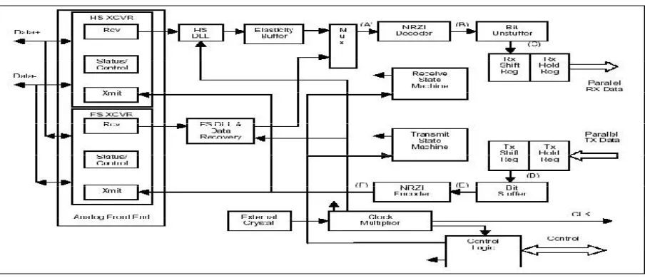
FIGURE 1 : Major Functional Block Diagram of UTMI Transceiver
II. DESIGN ASPECTS
Based on the above specifications provided by the USB 2.0 protocol the present UTMI has been designed . Further the UTMI is divided into two important modules which are the Transmitter module and the Receiver module. The design Specifications of these modules have been explained and integrated to get the top level Transceiver (UTMI) module.
II A. The Transmitter Module
The Transmitter is initiated by the Serial Interface Engine and SYNC pattern “01111110” is transmitted immediately . After six consecutive ‘1’s occur in the data stream a ‘0’ has to be inserted in the bit stream . Non Return to Zero Invert on 1 (NRZI -1) encoding technique is applied on the data[3]. At the End Of Pattern (EOP) two single ended zeroes (D+ and D lines are carrying zero for two clock cycles) and a bit ‘1’ have to be transmitted after each packet or after Serial Interface Engine suspends the transmitter[7]. The transmitter logic design facilitates the following functions like Sync transmission, holding the 8- bit Parallel data from SIE, Parallel to Serial conversion of data, Bit stuffing, NRZI encoding , Transmission of the data and EOP transmission on to the Serial bus.
II B. The Receiver Module
When the SYNC pattern is detected an intimation is send to the SIE. An error should be reported to the SIE when a ‘0’ is not detected after six consecutive 1’s . When EOP pattern is detected that should be intimated to the SIE[4] . The receiver logic design facilitates the following Functions Like SYNC detection, NRZI decoding, Bit un-stuffing, Serial to Parallel conversion of data, Receive error reporting and EOP detection[6].
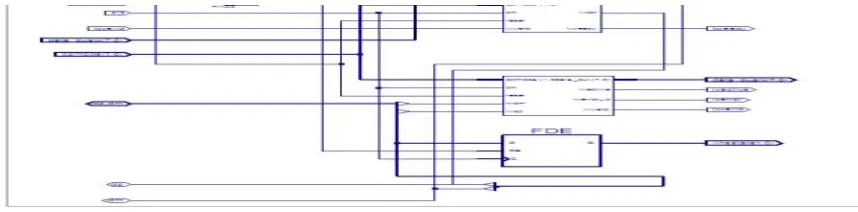
II C. The Transceiver Module
ISSN(Online): 2319-8753 ISSN (Print): 2347-6710
I
nternational
J
ournal of
I
nnovative
R
esearch in
S
cience,
E
ngineering and
T
echnology
(A High Impact Factor, Monthly, Peer Reviewed Journal) Visit: www.ijirset.com
Vol. 6, Issue 10, October 2017
the required UTMI Transceiver module logic has been verified with the functional Simulation then Synthesized and it is then Programmed to the targeted FPGA Device.
III. SIMULATON RESULTS
The three Major modules of the UTMI which are designed using VHDL as stated above are Simulated within the Xilinx based Model Simulator Environment.
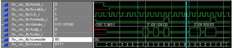
III A. The Transmitter Module
The Simulation results of UTMI transmitter Module which is designed using USB 2.0 Specifications is Shown in Figure 2. When TX valid signal goes high, encoded SYNC pattern “01010100”is transmitted and the signal Tx-ready is asserted. The data “10110100” present on the data ln bus is NRZI encoded and then transmitted on to the Tx-dp, Tx-dm lines. The signal Tx-ready goes low when the data is sampled by the TX hold register.
Figure 2: Simulation Result of UTMI Transmitter Module
III B. The Receiver Module
The Simulation result of UTMI Receiver Module which is designed using USB 2.0 Specifications is Shown in Figure 3 . When SYNC is detected Receive ( Rx) active is asserted. The data present on Rx dp, Rx dm lines are decoded, Converted from Serial to Parallel form and then sent to the SIE through data out bus by asserting Rx valid signal.
Figure 3: UTMI Receiver Module
III C. The Transceiver Module
ISSN(Online): 2319-8753 ISSN (Print): 2347-6710
I
nternational
J
ournal of
I
nnovative
R
esearch in
S
cience,
E
ngineering and
T
echnology
(A High Impact Factor, Monthly, Peer Reviewed Journal) Visit: www.ijirset.com
Vol. 6, Issue 10, October 2017
then sent to the SIE through rx data_bus by asserting Rx valid signal. Rx data_bus contains “00000000” since the transmitted data is fed back to the receiver.
Figure 4: Transceiver (UTMI) Module.
IV. FPGA IMPLEMENTATION
The Top order module, UTMI is Synthesized within the Xilinx Environment and it is programmed to the targeted SPARTAN 3E family of FPGA Device. The various levels of implementation such as Synthesis report, RTL View, Place and Route Report and Device Programming has been explained and visualized in the following sub sections.
Figure 5. Register Transistor Logic (RTL ) View of UTMI
V. CONCLUSION
The individual modules of UTMI have been designed using VHDL and verified functionally with the Model Sim . The UTMI Transmitter is capable of converting parallel data into serial bits, performing bit stuffing and NRZI encoding. The UTMI Receiver is capable of performing NRZI decoding bit un-stuffing and converting serial bits into parallel data. The functional simulation has been successfully carried out. The design has been synthesized using FPGA technology of Xilinx. This design is targeted to the device family_spartan3E,. The device belongs to the Vertex-E group of FPGAs from Xilinx. The UTMI is designed to support HS/FS, FS Only and LS Only UTMI implementations. The three options allow a single SIE implementation to be used with any speed USB transceiver. A vendor can choose the transceiver performance that best meets their needs.
VI. FUTURE SCOPE
ISSN(Online): 2319-8753 ISSN (Print): 2347-6710
I
nternational
J
ournal of
I
nnovative
R
esearch in
S
cience,
E
ngineering and
T
echnology
(A High Impact Factor, Monthly, Peer Reviewed Journal) Visit: www.ijirset.com
Vol. 6, Issue 10, October 2017
REFERENCES
[1] Charles H Roth “Digital system using VHDL”.2nd edition, Thomson publication
[2] Jayaram Bhasker “A VHDL Primer” 2nd edition, Prentice Hall publications
[3]Stephen Brown, Zvonko Vranesic “Fundamentals Digital logic with VHDL design”. 2nd edition, McGraw- Hill, Hardcover, Published July 2004 [4] Zainalabedin Navabi “Vhdl Analysis and Modeling of Digital Systems” 2nd edition, McGraw- Hill, Hardcover, Published January 1998 [5] William Stallings, “Data and Computer Communications” ,McGraw-Hill Publications.
[6] Andrew S.Tannenbaum, “Computer Networks”, Pearson publications.