IJEDR1502199
International Journal of Engineering Development and Research (www.ijedr.org)1202
Design, Simulation and Development of Bandpass
Filter at 2.5 GHz
Dipak C.Vaghela, A. K. Sisodia, N. M. Prabhakar Communication Engineering,
LJIET, Ahmedabad
________________________________________________________________________________________________________
Abstract - This paper is to design bandpass filter suitable with center at 2.5 GHz. This application is in the S band range at 2.5 GHz center frequency currently being used for Indian Regional Navigation Satellite System (IRNSS) receiver. The filter covers the centre frequency 2.5 GHz and the bandwidth is 80 MHz. This project was initiated with theoretical understanding of various types of filter and their applications. And suitable type was selected. It functions to pass through the desired frequencies within the range and block unwanted frequencies. In addition, filters are also needed to remove out harmonics that are present in the communication system. It was design and simulated using ADS (Advanced Design System) software
Keywords- Bandpass Filter, Chebyshev, Fractional Bandwidth, Advanced Design System (ADS)
________________________________________________________________________________________________________
I. INRODUCTION
Filter design depended on application requirnment. Application play very important role for filter design like which type of bandwidth require, ripple in passband, attenuation in stopband and center frequency. In this paper Filter is design for IRNSS application at 2.5GHz center frequency with 80MHz bandwidth with 0.1dB ripple level. Chebychev filter design type is used because it provide shaper cutoff in passbad.
II. CALCULATE FRACTION BANDWIDTH, NORMALIZED FREQUENCY AND NUMBER OF ORDER OF FILTER The centre operating frequency for the filter is 2.5 GHz with a bandwidth of 3.2%.The maximum ripple allowed in the pass band is 0.1 dB, and -20dB attenuation at 2.6GHz.According to the filter design specifications, Chebyshev response with a passband ripple of 0.1 dB can satisfy these requirements
Here, We have, 𝑓1= 2.46 GHz, 𝑓2= 2.54 GHz, so
△ = 𝜔2− 𝜔1 𝜔0
(1)
△= 0.032 Normalized frequency given by following method
𝜔 𝜔𝑐
= 1
△(
𝜔 𝜔𝑐
−𝜔𝑐
𝜔)
(2)
𝜔 𝜔𝑐
= 2.451923
Next step for designing any Chebychev filter is to determine the order of the filter. The filter order is number of inductive and capacitive elements that should be included in the filter design. This can be done by following formulation
𝑛 =
cosh−1√10
𝐿𝑇
10−1
𝐾 − 1
cosh−1(𝜔
𝜔0)
(3)
𝑛 ≅ 3
IJEDR1502199
International Journal of Engineering Development and Research (www.ijedr.org)1203
III. CALCULATE LOW-PASS FILTER PROTOTYPES AND LUMPED ELEMENTS VALUES OF THE BANDPASS FILTERThe following equations are used to calculate the Element values for equal-ripple low-pass filter prototypes (0.1 dB ripple)
𝑎𝑘 = sin (
(2𝑘 − 1)𝜋
2 ∗ 𝑛 )
(4)
𝑏𝑘= 𝛾2+ 𝑠𝑖𝑛2(
𝑘𝜋
𝑛)
(5)
𝛽 = ln [coth ( 𝐿𝑎𝑟 17.37)]
(6)
𝛾 = sinh ( 𝛽
2 ∗ 𝑛)
(7)
𝑔0= 1
(8)
𝑔1=
2 ∗ 𝑎1
𝛾
(9)
𝑔𝑘 =
4 ∗ 𝑎𝑘−1∗ 𝑎𝑘
𝑏𝑘−1∗ 𝑔𝑘−1
(10)
gn+1= 1
(11) In above equetions k = 1,2,3,4……
Now we can get following table for 0.1 dB ripple level with the help of equation (4) to (11) for various
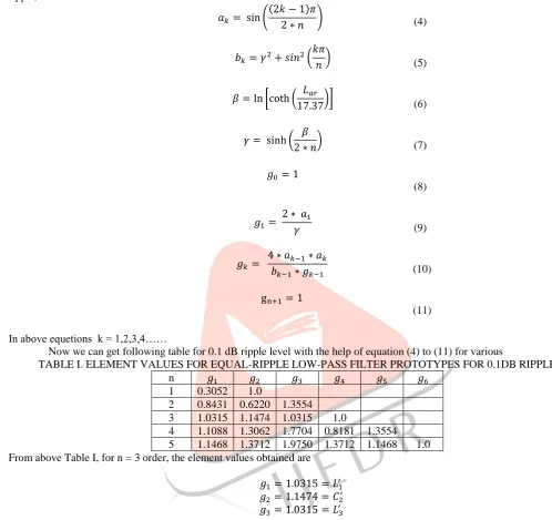
TABLE I. ELEMENT VALUES FOR EQUAL-RIPPLE LOW-PASS FILTER PROTOTYPES FOR 0.1DB RIPPLE
n 𝑔1 𝑔2 𝑔3 𝑔4 𝑔5 𝑔6
1 0.3052 1.0
2 0.8431 0.6220 1.3554 3 1.0315 1.1474 1.0315 1.0
4 1.1088 1.3062 1.7704 0.8181 1.3554 5 1.1468 1.3712 1.9750 1.3712 1.1468 1.0 From above Table I, for n = 3 order, the element values obtained are
𝑔1= 1.0315 = 𝐿1′
𝑔2= 1.1474 = 𝐶2′
𝑔3= 1.0315 = 𝐿3′
Lumped Values of the Bandpass Filter calculate as following method. Now we can calculate L and C component value as following parameter. The Lumped values of the Band pass filter after frequency and impedance scaling are given by
For Series L&C
LK=
Z0∗ L′K
ω0∗△
(12)
𝐶𝐾=
△ 𝑍0∗ 𝐿′𝐾∗ 𝜔0
(13)
IJEDR1502199
International Journal of Engineering Development and Research (www.ijedr.org)1204
𝐿𝐾=
△∗ 𝑍0
𝜔0∗ 𝐶𝐾′
(14)
𝐶𝐾=
𝐶𝐾′
𝑍0∗ 𝜔0 ∗△
(15)
Where𝑍0= 50 Ω, Δ = 0.032 and 𝑓0= 2.5 GHz
IV.ADS SIMULATION OF LC COMPONENTS AND RESULT
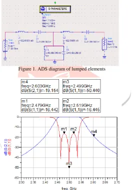
Now put all values if Series and Shunt elements value in Following Bandpass filter design in ADS (Advanced Design System)
Figure 1. ADS diagram of lumped elements
Figure 2. S-parameter simulation schematic of filter
Practically, it is not possible to design this bandpass filter at high frequency in such LC components, for that we can used Microstrip line as a transmission line
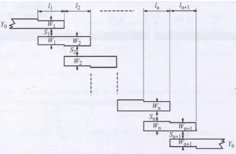
V. PARALLEL COUPLED MICROSTRIP FILTER
IJEDR1502199
International Journal of Engineering Development and Research (www.ijedr.org)1205
Figure 3. Common structure of microstrip parallel coupled line bandpass filterThe strips are arranged parallel close to each other, so that they are coupled with certain coupling factors. We use the following equations for designing the parallel-coupled filter
𝐽01
𝑌0
= √𝜋 ∗ 𝐹𝐵𝑊
2 ∗ 𝑔0∗ 𝑔1
(16)
For j=1 to n-1:
𝐽𝑗,𝑗+1
𝑌0
=𝜋 ∗ 𝐹𝐵𝑊
2
1
√𝑔𝑗∗ 𝑔𝑗+1
(17)
𝐽𝑛,𝑛+1
𝑌0
= √ 𝜋 ∗ 𝐹𝐵𝑊
2 ∗ 𝑔𝑛∗ 𝑔𝑛+1
(18)
Where 𝑔0,𝑔1… 𝑔𝑛 are the element of a ladder-type low-pass prototype with a normalized cut-off Ω𝑐 = 1, and FBW is the
fractional bandwidth of band-pass filter. 𝐽𝐽,𝐽+1 are the characteristic admittances of J-inverters and 𝑌0 is the characteristic admittance
of the terminating lines. The equation above will be used in end-coupled line filter because the both types of filter can have the same low-pass network representation. However, the implementation will be different. To realize the J-inverters obtained above, the even- and odd-mode characteristic impedances of the coupled microstrip line resonators are determined by
For j=0 to n
(𝑍0𝑒)𝑗,𝑗+1=
1 𝑌0
[1 +𝐽𝑗,𝑗+1 𝑌0
+ (𝐽𝐽,𝐽+1 𝑌0
)2]
(19)
(𝑍0𝑜)𝑗,𝑗+1=
1 𝑌0
[1 −𝐽𝑗,𝑗+1 𝑌0
+ (𝐽𝐽,𝐽+1 𝑌0
)2]
(20)
TABLE II. CALCULATED VALUES OF EVEN AND ODD RESISTANCES
Stage(i,i+1) 𝑍0𝑒Ω 𝑍0𝑜Ω
1,4 63.4729 41.3994
2,3 52.4178 47.7975
The next step of the filter design is to find the dimensions of coupled microstrip lines that exhibit the desired even mode and odd-mode impedances. Firstly, we determine the equivalent single microstrip shape ratios 𝑊
𝐻 essentially responsible to relate
IJEDR1502199
International Journal of Engineering Development and Research (www.ijedr.org)1206
𝑍0𝑠𝑜=(𝑍0𝑜)𝑗,𝑗+1
2
(21)
𝑍0𝑠𝑒=
(𝑍0𝑒)𝑗,𝑗+1
2
(22)
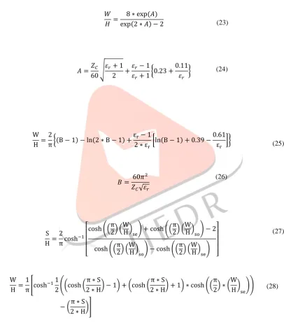
For a single microstrip line, The approximate expressions for W/h (Figure 1) in terms of 𝑍𝑐 and 𝜀𝑟, derived by Wheeler
and Hammerstad, are available For 𝑊
𝐻≤ 2
𝑊
𝐻 =
8 ∗ exp (𝐴) exp(2 ∗ 𝐴) − 2
(23)
Where
𝐴 =𝑍𝐶
60√
𝜀𝑟+ 1
2 +
𝜀𝑟− 1
𝜀𝑟+ 1
{0.23 +0.11
𝜀𝑟
}
(24)
For 𝑊
𝐻≥ 2
W
H =
2
π{(B − 1) − ln(2 ∗ B − 1) +
εr− 1
2 ∗ εr
[ln(B − 1) + 0.39 −0.61
εr
]} (25)
Where
𝐵 = 60𝜋
2 𝑍𝐶√𝜀𝑟 (26) S H= 2 πcosh −1 [
cosh ((π2) (WH)
se) + cosh ((
π 2) (
W
H)so) − 2
cosh ((π2) (WH)
so) − cosh ((
π 2) (
W H)se) ]
(27) W H = 1 π[cosh −11
2((cosh (
π ∗ S
2 ∗ H) − 1) + (cosh (
π ∗ S
2 ∗ H) + 1) ∗ cosh (( π 2) ∗ (
W H)se
))
− (π ∗ S 2 ∗ H)]
(28)
TABLE III. CALCULATED DIMENSIONS OF TRANSMISSION LINE SECTIONS Line
Description W(mm) L(mm) S(mm)
50 ohm-line 2.2910 16.4079 - Coupled line
1 and 4 2.0253 16.5025 0.6110 Coupled line
IJEDR1502199
International Journal of Engineering Development and Research (www.ijedr.org)1207
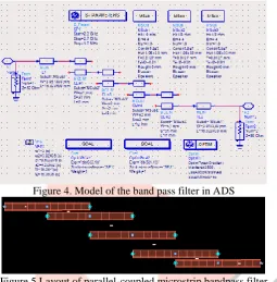
VI. DESIGN SPECIFICATIONThe filter was modelled in ADS as shown in Figure 4. Using LineCalc tool in ADS, the dimension of the microstrip line viz. length (L), width (W) and gap(S) To match with the 50 ohm circuit, MLIN (Microstrip Line) components are added to both sides of the filter whose characteristic impedance is 50 ohm The Parameters of the substrate set in MSub controller are:
1) H: substrate thickness (1.2 mm)
2) Er: substrate relative dielectric constant (4.4) 3) Cond: metal conductivity (5.8e7)
4) Hu: upper ground substrate spacing (1.0E+33mm) 5) T: the thickness of metal layer (0.0127 mm) 6) TanD: dielectric loss tangent (0.01)
Figure 4. Model of the band pass filter in ADS
IJEDR1502199
International Journal of Engineering Development and Research (www.ijedr.org)1208
Figure 6. Momentum simulation resultsVII. Fabrication Results Analysis
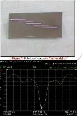
Fabrication is done by Etching technique with FR4 substrate material, and its model is following
Figure 7. Fabricate bandpass filter model
IJEDR1502199
International Journal of Engineering Development and Research (www.ijedr.org)1209
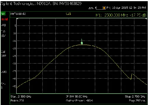
Figure 9. Hardware result of S(2,1)In Figure 9, while measurement of S(2,1) using VNA also consider both cables loss which is -14.606dB cable loss.so we can compare schematic and practical results as following Table IV
TABLE IV. COMPARISON OF SCHEMATIC AND PRACTICAL RESULTS Index Return Loss
S(1,1)dB
Insertion loss S(2,1)dB
Schematic Result -20.64 -4.780
Practical Result -20.63 -3.144
VIII. CONCLUSION
Designing a Parallel-Coupled Bandpass filter for IRNSS Application, has been presented. For the selected center frequency of 2.5 GHz and on a substrate, we select FR4 with dielectric constant 4.4, because it is easily available in market, less cost and get very good result. We get result as insertion loss around -4.87dB and return loss is -20.64dB in passband with 80 MHz bandwidth in schematic, and insertion loss is around -3.144dB and return loss is -20.63dB in hardware and which is desirable.
REFERENCES
[1] Min Zhang; Yimin Zhao; Wei Zhang, "The simulation of microstrip Band Pass Filters based on ADS," Antennas, Propagation & EM Theory (ISAPE), 2012 10th International Symposium, pp. 909-912, Oct. 2012, ISBN: 978-1-4673-1799-3
[2] Seghier, S.; Benahmed, N.; Bendimerad, F.T.; Benabdallah, N.,"Design of parallel coupled microstrip bandpass filter for FM Wireless applications," Sciences of Electronics, Technologies of Information and Telecommunications (SETIT), 2012 6th International Conference, pp.207-211, March.2012,ISBN: 978-1-4673-1657-6
[3] Ma, Jun; Sun, Zhengwen; Chen, Yong, "Design and simulation of L-band wideband microstrip filter," Information Science and Technology (ICIST), 2013 International Conference, pp. 183-186, March 2013,ISBN: 978-1-4673-5137-9
[4] Bey-Ling Su; Ray Yueh-Ming Huang, "5.8 GHz bandpass filter design using planar couple microstrip lines," Communications, Circuits and Systems, 2004.ICCCAS 2004. 2004 International Conference on, vol.2, pp. 1204-1207, June 2004, ISBN: 0-7803-8647-7
[5] Naghar, A.; Aghzout, O.; Vazquez Alejos, A.; Garcia Sanchez, M.; Essaaidi, M., "Development of a calculator for Edge and Parallel Coupled Microstrip band pass filters," Antennas and Propagation Society International Symposium (APSURSI), 2014 IEEE , pp. 2018-2019, July 2014, ISBN: 978-1-4799-3538-3
[6] Lolis, L.; Pelissier, M.; Bernier, C.; Dallet, D.; Begueret, J-B, "System design of bandpass sampling RF receivers," Electronics, Circuits, and Systems, 2009. ICECS 2009. 16th IEEE International Conference, pp. 691-694, Dec.2009,ISBN: 978-1-4244-5090-9
[7] E. O. Hammerstard, “Equations for microstrip circuit design,” in Proceedings of the European Microwave Conference, Hamburg, Germany, pp. 268–272, 1975
[8] H. Wheeler, “Transmission line properties of parallel strips separated by a dielectric sheet”, IEEE Trans., MTT-13, pp. 172-185, 1965, ISSN: 0018-9480
[9] D. M. Pozar, Microwave Engineering, 3rd Ed. New York: Wiley, pp. 389-426, 2005
[10] Annapurna Das and Sisir K Das, “Microwave Engineering”, Mac Graw Hill, pp. 279-310, 2001
[11] J. S. Hong, M. J. Lancaster, “Microstrip Filter for RF/Microwave Applications”, A Wiley Interscience Publication, Canada, pp. 29-158, 2001.