University of Windsor University of Windsor
Scholarship at UWindsor
Scholarship at UWindsor
Electronic Theses and Dissertations Theses, Dissertations, and Major Papers
2016
DESIGN OF MULTI-VALUED LOGIC CELLS USING
DESIGN OF MULTI-VALUED LOGIC CELLS USING
SINGLE-ELECTRON DEVICES
ELECTRON DEVICES
Lin Li
University of Windsor
Follow this and additional works at: https://scholar.uwindsor.ca/etd
Recommended Citation Recommended Citation
Li, Lin, "DESIGN OF MULTI-VALUED LOGIC CELLS USING SINGLE-ELECTRON DEVICES" (2016). Electronic Theses and Dissertations. 5743.
https://scholar.uwindsor.ca/etd/5743
DESIGN OF MULTI-VALUED LOGIC CELLS
USING SINGLE-ELECTRON DEVICES
By
Lin Li
A Thesis
Submitted to the Faculty of Graduate Studies
through Electrical and Computer Engineering
in Partial Fulfillment of the Requirements for
the Degree of Master of Applied Science at the
University of Windsor
Windsor, Ontario, Canada
DESIGN OF MULTI-VALUED LOGIC CELLS
USING SINGLE-ELECTRON DEVICES
By
Lin Li
APPROVED BY:
______________________________________________
Dr. Y. Wang, Department of Economics
______________________________________________ Dr. E. Abdel-Raheem,
Department of Electrical and Computer Engineering
______________________________________________ Dr. Chunhong Chen, Advisor
Department of Electrical and Computer Engineering
Author‘s Declaration of Originality/Previous
Publication
I. Co-Authorship Declaration
I hereby declare that this thesis incorporates material that is result of joint research, as
follows:
In all cases, the primary contributions, derivations, experimental setup, data analysis and
interpretation were performed by the author through the supervision of Dr. C. Chen. In
addition to supervision, Dr. C. Chen provided the author with the project idea, guidance,
and financial support.
I am aware of the University of Windsor Senate Policy on Authorship and I certify that I
have properly acknowledged the contribution of other researchers to my thesis, and have
obtained written permission from each of the co-author(s) to include the above material(s)
in my thesis.
I certify that, with the above qualification, this thesis, and the research to which it refers,
is the product of my own work.
II. Declaration of Previous Publication
This thesis includes 3 original papers that have been previously published/ submitted for
publication in peer reviewed journals, as follows:
Chapter
Chapter 3 L. Li and C. Chen, “An analytical
model for NDC blocks with
single-electron tunneling,” in
Proceedings of the IEEE International
Conference on Nanotechnology, July
2015, pp. 448-451.
“published”
Chapter 4 L. Li and C. Chen,” Modeling and
Application for
Negative-Differential-Conductance
Devices with Single-Electron
Technology”
"Submitted"
Chapter 5 L. Li and C. Chen, ” An Area-Efficient
Ternary Full Adder Using Hybrid
SET-MOS Technology”
"Submitted"
I certify that I have obtained a written permission from the copyright owner(s) to
include the above published material(s) in my thesis. I certify that the above material
describes work completed during my registration as graduate student at the University of
Windsor.
anyone’s copyright nor violate any proprietary rights and that any ideas, techniques,
quotations, or any other material from the work of other people included in my thesis,
published or otherwise, are fully acknowledged in accordance with the standard
referencing practices. Furthermore, to the extent that I have included copyrighted material
that surpasses the bounds of fair dealing within the meaning of the Canada Copyright Act,
I certify that I have obtained a written permission from the copyright owner(s) to include
such material(s) in my thesis.
I declare that this is a true copy of my thesis, including any final revisions, as
approved by my thesis committee and the Graduate Studies office, and that this thesis has
Abstract
This thesis proposes a new single-electron tunneling based NDC block and develops an
analytical model which can be used for related circuit designs and/or their performance
optimization. A piece-wise model is used to describe the I-V characteristics of the
proposed NDC block. Four applications based on this NDC block are proposed: (1)
Multiple-valued logic static memory cell (2) Schmitt trigger (3) Three-stage ring
oscillator (4) ternary full adder using hybrid single-electron transistor and MOS
technology. Simulation was done using Cadence Spectre simulator with 180nnm CMOS
A Sincere Dedication
Acknowledgements
I would like to express my gratitude to my supervisor Dr. Chunhong Chen for his
useful comments, remarks and engagement through the learning process of this Master
thesis. I have learned many thing since I became Dr. Chunhong Chen‘s student. He
spends very much time instructing me how to write a paper, how to search literature and
how to collect data. My thanks also go to Dr. E. Abdel-Raheem and Dr Y Wang for their
constructive comments. Furthermore I would like to thank Ran Xiao for introducing me
to the topic as well for the support on the way. Special thanks are given to Department of
Electrical and Computer Engineering. Most of my theoretical foundations are built in here.
Also, I like to thank the participants in my survey, who have willingly shared their
precious time during the process of interviewing. I would like to thank my loved ones,
including my parents and brother, who have supported me throughout entire process, both
by keeping me harmonious and helping me put pieces together. I will be grateful forever
for your love. Without their support, it would have been impossible for me to finish my
Table of Contents
Author‘s Declaration of Originality/Previous Publication... iii
Abstract... vi
A Sincere Dedication... vii
Acknowledgements ... viii
List of Tables... xii
List of Figures... xiii
List of Abbreviations... xv
CHAPTER I. Introduction 1.1 Background and Motivation...1
1.2 Thesis organization...5
II. Background of nano electronic Design 2.1 CMOS Scaling Limits ………...7
2.2 Coulomb blockade effect ...8
2.3 Orthodox Theory ………...9
2.4 Monte Carlo Simulation...………...10
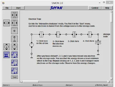
2.5 SIMON—A Simulator for Single-Electron Tunnel Devices and Circuits ...11
III. An Analytical Model for NDC Blocks with Single-Electron Tunneling 3.1 Previous Works ………...14
3.1.1 Three-Junction NDC Block ...14
3.2.1 Four-Junction NDC Block ...15
3.2.2 Piece-Wise Model ...16
3.3 Impacts of Circuit Parameters and Temperature ………...21
3.4 Simulation Results and Discussion ……….25
IV. Modeling and Application for Negative-Differential-Conductance Devices with Single-Electron Technology 4.1 Previous Works …...27
4.1.1 G4-FET Voltage-Controlled NDR Device ...27
4.1.2 LC Oscillator ...28
4.1.3 Schmitt Trigger...29
4.2 Multiple-Valued Logic Memory Cells ...30
4.2.1 Schematic Circuit………...30
4.2.2 Write Operation for Memory Cell...32
4.2.3 Impacts of Circuit Parameters …...32
4.2.4Temperature Effects ……….…………..………34
4.3 Schmitt trigger ………...36
4.4 Oscillator Using NDC Inverter ...40
V. An Area-Efficient Ternary Full Adder Using Hybrid SET-MOS Technology 5.1 Previous works ...42
5.1.1 TFA based on CNTFET………...42
5.1.2 TFA using the Ternary Adiabatic Logic (TAL)...43
5.3 T-Gate ...44
5.4 Proposed TFA ...47
5.5 Simulation Results with Discussions...49
VI. Conclusion and Future Work 6.1 Conclusion …...55
6.2 Future work ...55
References ...57
Appendix A: Code of NDC Model…...60
Permission to Use Previously Published /Submitted Papers ……….76
List of Tables
5.1 Examples of ternary functions using T-gate …...49
List of Figures
1.1 A plot of CPU transistor counts...2
1.2 A plot of new technology generation introductions (1975–2005)...3
1.3 Negative Differential resistance characteristic curve…...5
2.1 Coulomb blockade in a single tunnel junction ………...8
2.2 Interface of SIMON …...12
3.1 The three junctions SET-based NDC block …...14
3.2 The five junctions SET-based NDC block …...15
3.3 The proposed multiple-peak SET-based NDC block …...16
3.4 The state transition diagram for Fig 3.3 ………...17
3.5 Simulation results of Fig 3.3 …...21
3.6 Curves of tunnel rate when T=0 and T>0 …...22
3.7 Simulation results of Fig 3.3 (T=0) …...23
3.8 Simulation results of Fig 3.3 (T>0) …...25
3.9 Simulation results of Fig 3.3 (T>0 and Cg2=35Cj) …...26
4.1 Conventional 2-terminal JFET NDR device and 4-terminal G4-NDR …...28
4.2 Schematic of LC oscillator …...29
4.3 Schematic of Schmitt Trigger …...30
4.4 Schematic for the memory cell and simulation results …...31
4.5 Logic voltages for the memory cell using two-peak NDC elements …...33
4.6 Impacts of parameters on the memory’s I-V characteristics …...34
4.8 Schematic circuit of Schmitt trigger and its voltage transfer characteristic…...37
4.9 Simulation results of the proposed Schmitt trigger …...39
4.10 Schematic circuit of ring oscillator with feedback and Output waveform…...40
5.1 A SET-MOS literal gate and its circuit symbol …...44
5.2 The proposed multiple-peak SET-based NDC block …...46
5.3 Schematic of the proposed ternary full adder ……….…...48
5.4 Simulation results of the proposed TFA …...51
5.5 The average power vs frequency …...52
List of Abbreviations
CMOS – Complementary Metal Oxide Semiconductor
MOSFET – Metal Oxide Semiconductor Field Effect Transistor
MVL – Multiple-Valued Logic
NDC – Negative Differential Conductance
PVCR – Peak to Valley Current Ratio
CB- Coulomb blockade
RTD -- Resonant Tunneling Diode
SED – Single Electron Device
SET -- Single Electron Transistor
TAL- ternary adiabatic logic
TFA-ternary full adder
Chapter 1
Introduction
1.1 Motivation and background
Complementary metal–oxide–semiconductor (CMOS) technology is predicted to
confront significant technology limitations, which can slow the development of the
integrate circuits, and the CMOS technology will reach to the crisis by the year 2020. Due
to these limits, it is probable that CMOS will share its domination on the future integrated
circuits (ICs) with the fundamentally new devices that use a few electrons, such as single
electron transistors (SETs). In the past few decades, reducing power consumption used to
be the primary task in chip designs to meet Moore’s law. Figure.1.1 shows a plot of CPU
transistor counts against dates of introduction. To deal with this issue, many
ultralow-power devices have been explored. The power dissipation of single-electron
transistors is ultralow; since it works with only one or a few electrons during switching
operations. The drain current of SET is approximately three to four orders of magnitude
lower than the traditional CMOS technology, which gets further reduction because of
energy quantization effects. Hence, the practical implementation of SETs in modern very
large scale integration (VLSI) technology necessitates hybrid CMOS-SET circuit logic.
Therefore, we cannot use only single electron transistor with semiconductor technique as
Fig 1.1 a plot of CPU transistor counts [17]
On the other hand, rapid progress in the fabrication technology of Silicon nano
devices has pushed the device dimension toward 1-100nm length scale, which renders the
basic working principles of the CMOS devices more dependent upon quantum effects and
doping fluctuations. When device dimensions are scaled down to a few nanometers,
quantum effects such as single electron tunneling and energy quantization lead to
interesting new device characteristics that can be exploited to create extremely compact
Fig 1.2 a plot of new technology generation introductions (1975–2005) [17]
The SET is one type of nanoscale electronic devices based on quantum tunneling
and coulomb blockade effect, where one or more coulomb islands are sandwiched
between two tunnel junctions which connect respectively with the drain electrode and the
source electrode, and capacitive coupled with one or more gate electrodes.
Coulomb blockade of SETs is based on the controllable transfer of single electrons
through small conducting, which called "islands". By taking advantage of the Coulomb
blockade effect in controlling the transfer of individual electrons, the SET could lead to
single-electron logic devices. Most single electron devices, such as Single-electron
transistor models, are based on the orthodox theory of the single-electronics.
From the discussions of above, we can find that the SET has attracted attention as a
candidate for future VLSI mainly due to these three reasons: nanoscale size, ultralow
SET is a promising candidate device to substitute the CMOS, it also has its disadvantages,
such as a poor driving capability, poor threshold control due to the involvement of only
one or a few electrons in the switching process. Therefore, the conduction mechanism of
the conventional CMOS-based logic is not applicable to SETs [1].
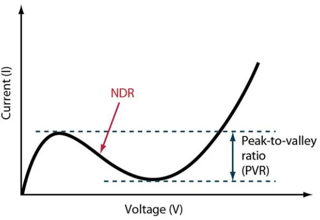
Negative differential conductance (NDC) block is a subcircuit that shows both
positive and negative differential conductance in its I-V characteristics (Fig.1.3) [2, 3].
NDC blocks have been widely used for applications that essentially require signal
amplification, hysteresis and/or memory (such as Schmitt triggers, amplifiers, oscillators,
and logic memory circuits) [4]. NDC blocks can be implemented using traditional CMOS
technology, emerging nano-scale devices such as SET, or hybrid CMOS-SET framework.
However, research shows that SET-based implementations are desirable due to their high
integration density and/or low power consumption. This is especially true for applications
that require multiple-peak NDC characteristics (such as multiple-valued memory cells) as
SET devices demonstrate their unique Coulomb blockade oscillations. Indeed, recent
work reported NDC implementations using three tunnel junctions for binary logic or five
Fig 1.3 Negative Differential resistance characteristic curve
1.2 Organisation of this thesis
This thesis is organized as follows. Chapter 2 provides a background on the Nano
electronic design and discusses the key concerns of SET technology. Later some basic
information is presented for the Monte Carlo simulator for SET.
Chapter 3 presents a new single-electron tunneling based NDC block, and develops
an analytical model which can be used for related circuit designs and/or their performance
optimization. Simulation results are provided to show the effectiveness of the model with
considerations of temperature effects.
Chapter 4 deals with different applications for SET-based NDC devices. A
shown to verify the effectiveness of the proposed approach with considerations of
temperature effects. In chapter 5, we propose a novel design of ternary full adder (TFA)
using hybrid SET and MOS technology. The proposed circuit is evaluated using the
Cadence Spectre simulator with 180nm CMOS technology and SET macro models under
various test conditions. Results show that the proposed TFA dramatically reduces the
number of transistors required with little or no loss in energy efficiency.
Chapter 6 concludes the thesis along with some future research works. The appendix
Chapter 2
Background of Nano electronic Design
2.1 CMOS Scaling Limits
The continuous shrinking of MOSFET device dimensions has been the main catalyst
for the stunning growth of the modern microelectronic industry. The minimum feature
size is fast approaching 100nm in the next decade with switching charges containing 1000
or less electrons. Moore’s law is expected to break down for conventional
microelectronics for a variety of reasons [8].
Physical limit:
1) Thermal limit: E >>kBT or E ~ 100 kBT
Where E is Energy necessary to write a bit, kBT is thermal energy.
2) Quantum limit: ΔEΔt >> h or E/f ~ 100 h (h – Planck’s constant = 6.6×10⁻³⁴ J· S, f –
circuit frequency).
Technological limit:
1) Power dissipation limit: E· f· n ~ 100W/cm2 (maximum tolerable ΔEΔt >> h) where n
- device density.
2) Process variations, second-order effects and design complexity.
Economic limit:
The increasing costs of new semiconductor fabrication is making questionable the future
2.2
Coulomb
blockade effect
The Coulomb blockade effect is a phenomenon in which electrons cannot tunnel into
the junction when the charging energy of a single electron is much larger than the thermal
energy. Figure 2.1 shows the coulomb blockade in a single tunnel junction [9].
Coulomb blockade
I
U -e/2c
e/2c
U
Rt,Ct
Fig 2.1 coulomb blockade in a single tunnel junction
The electron addition energy (EA —the amount of work that has to be done in order to add
one extra electrone into it) is measured as
(2.1)
Where C is a small spherical electro neutral conductor of capacitanceECis the charging energy
(e2/C for a spherical conductor) and EKis the quantum kinetic energy (usually neglected if
the feature size is more than 1 nm).
Therefore, in a single-electron system, the electrons need a minimum energy for
electron can tunnel through the junction, which means the device enters into off state;
such a situation is the Coulomb blockade.
2.3
Orthodox Theory
Throughout the history of single electronics, a unique guiding role has been played
by a simple but very effective “orthodox” theory. For a particular case, this theory was
developed by Kulik and Shekhter. The theory makes the following major assumptions.
First of all, the electron energy quantization inside the conductors is ignored. It
means that this assumption is valid when Ek >>kBT or Ec>>Ek .
Then, the time of electron tunneling through the barrier also can be ignored
comparing with other time scales (including the interval between neighboring tunneling
events).
Coherent quantum processes consisting of several simultaneous tunneling events are
ignored. This assumption is valid if the resistance of all the tunnel barriers of the system
is much higher than the quantum unit of resistance RQ
2.4
Monte Carlo
Simulation
The orthodox single-electron theory yields a tunnel rate equation for any junction in
a large circuit [11]:
) 1
( )
(
2 kT
F j n B
e
R
e
F
V (2.3)
Where kBT is the thermal energy, e is the electron charge, and ΔF is the change in free
energy when an electron tunnels through the junction, which can be written as ΔF = e (Vj
– Vc), where Vj is the junction voltage and Vc is the critical voltage given by Vc = e/
(2Ctotal) with Ctotal being the total capacitance seen from the tunnel junction [9].
If this tunnel rate is coupled into a Poisson process the fundamental building blocks
for a Monte Carlo based simulation are assembled. The Poisson distribution can be
rearranged to yield
(2.4)
Where r is an evenly distributed random number from the interval [0, 1] and t is the time
at which an electron tunnels through the junction.
The Monte Carlo procedure is as follows. Step one, all possible tunnel events with
their particular tunnel rates concreting random tunnel times are computed for all
events. Then, the event with the smallest t will happen first and is taken as the winner of
the Monte Carlo step. At same time, charges and voltages are updated on all circuit nodes.
New tunnel rates are calculated and a new winner is determined through stochastic
can be calculated.
Monte Carlo method is superior to other approaches due to it gives better transient
and dynamic characteristics of SET circuits. The master equation deals with average
probabilities and transition rates, which paint a more macroscopic picture [8]. In that
method, it is not required to find the relevant states before one can start with the actual
simulation as in the case of a master equation. Monte Carlo method is easy to trade
accuracy with simulation time, and therefore, one can quickly achieve approximate
results of very large circuits.
Nevertheless, there is one major disadvantage of the Monte Carlo method. When it
comes to simulating tunneling, a plain Monte Carlo approach has its limitations.
Tunneling is a very rare process which is difficult to resolve by a Monte Carlo method. It
demands very long simulation times. We tackled this problem by implementing a new
algorithm that combines the Monte Carlo and master equation methods.
2.5 SIMON—A Simulator for Single-Electron Tunnel Devices
and Circuits
SIMON is a single-electron tunnel device and circuit simulator that is based on a
Monte Carlo method. Transient and stationary simulation is offered by SIMON for
arbitrary circuits consisting of tunnel junctions, capacitors, and voltage sources of three
kinds: constant, piecewise linearly time dependent, and voltage controlled. Tunneling can
be simulated either with a plain Monte Carlo method or with a combination of the Monte
we discuss the essential problem of random background charge and present possible
solutions [8].
Chapter 3
An Analytical Model for NDC Blocks with Single-
Electron Tunneling
Negative differential conductance block is a subcircuit that shows both positive and
negative differential conductance in its I-V characteristics. NDC blocks have been widely
used for applications that essentially require signal amplification, hysteresis and/or
memory (such as Schmitt triggers, amplifiers, oscillators, and logic memory circuits).
NDC blocks can be implemented using traditional CMOS technology, emerging
nano-scale devices such as single-electron tunneling, or hybrid CMOS-SET framework.
However, research shows that SET based implementations are desirable due to their high
integration density and/or low power consumption. This is especially true for applications
that require multiple-peak NDC characteristics (such as multiple-valued memory cells) as
SET devices demonstrate their unique Coulomb blockade oscillations. Indeed, recent
work reported NDC implementations using three tunnel junctions for binary logic or five
junctions for multiple-valued logic. However, there is a lack of analytical models for
NDC blocks so far, making it very difficult to perform circuit analysis and/or
3.1 Previous Works
3.1.1 Three-junction NDC block
The schematic circuit diagram of the NDC device based on a SET is shown in Fig
3.1. The right island forms a SET, allowing a current to flow between voltage source and
ground through the left island, which acts as an electron box. The capacitors CG are
capacitances coupled with islands and CD, CN and CS are the capacitances of tunnel
junctions [5].
CG
CG
CD,RD CM,RM CS,RS
Drain Source
Fig 3.1 the three junctions SET-based NDC block
3.1.2 Three-junction NDC block
Fig 3.2 shows the proposed multiple-peak NDC structure, which consists of four
islands. The islands 1 and 3 form two cross-coupled single-electron transistors (SET 1
and SET 2). The capacitors Cg and Coare capacitances coupled with the islands, and Cd,
Cg
Cg
Cd,Rd Ca,Ra Cm,Rm
Drain Source
Cb,Rb
Cs,Rs
Co
Fig 3.2 the five junctions SET-based NDC block
3.2 The Proposed Model
3.2.1Four-Junction NDC Block
Fig 3.3 shows a four-junction NDC block with symmetric structure, where Cjand Rj
are the capacitance and resistance of each tunnel junction, and Cg1and Cg2can be
adjusted to obtain a different number of peaks in the NDC I-V characteristic.
Cg2
Cg1
Cj1 Cj2 Cj3 Cj4
Island 1
Island 2 Island 3
Island 4
Island 5
3.2.2 Piece-Wise Model
To calculate the island voltages in Fig 3.3, we first define an island capacitance
matrix as follows:
C (3.1)
where the diagonal element cii (i = 1~4) represents the total capacitance of island i, while
the cij (i, j = 1~4 and i ≠ j) represents the negative value of capacitance between islands i
and j. Assume the charges on islands 1 through 4 are q1, q2, q3 and q4, respectively.
For a given input voltage V1 at island 1, the voltages on other islands (i.e., V2, V3 and
V4) are determined by
Q = CV (3.2)
Where Q = [q1q2 q3 q4] T and V = [V1V2 V3 V4] T.
If we further define a specific charge distribution on islands 2, 3 and 4 (i.e., { q2 q3
q4}) as a state {n}, then the tunnel rate for the tunneling that causes the state transition
from state n to the next state is given by [7]
2 ( )
(1 B )
n F
k T j
F
e R e
V (3.3)
where Rj is the tunnel junction resistance, kBT is the thermal energy, e is the electron
charge, and ∆F is the change in free energy when an electron has tunneled through the
tunnel junction, and can be written as ∆F = e (Vjun – Vcr), where Vjun is the junction
voltage and Vcr is the critical voltage given by Vcr = e/ (2Ctotal) with Ctotal being the total
Fig 3.4 the state transition diagram
If a certain voltage V1 causes a continuous state transition, there will be a static
current flowing through the NDC block. Otherwise, the block will enter a Coulomb
blockade (CB) with no current. It is found that when the continuous state transition occurs,
the following state transition cycles will occur: {7e, 0, −3e} → {8e, 0, −3e} → {7e, e,
−3e} → {7e, 0, −2e} → {7e, 0, −3e}, or {7e, 0, −3e} → {8e, 0, −3e} → {7e, e, −3e} →
{7e, 0, −2e} → {8e, 0, −2e} → {8e, 0, −3e} → {7e, 0, −3e}. This process is described by
the state transition diagram shown in Fig 3.4. Using Markov chain analysis on Fig 3.4
[11], the state probabilities (denoted by P1~P5) can be found using the following
1 1 4 4 _1
2 2 1 1 5 5
3 3 2 2
3 3 4 4 _1 4 _ 2
5 1 * * * * * * * * * ( ) 1 i i P P
P P P
P P P P P
(3.4)Then the islands’ state probabilities are derived by using Markov chain analysis [8].
P1= (3.5)
P3= (3.6)
P5= (3.7)
P4= (3.8)
P2=1-(P1+P3+P4+P5) (3.9)
The static current can be calculated at any tunnel junction (say, the first junction
between islands 1 and 2) by combining the tunnel rate(s) with state probabilities as:
I I1 ( P1* 1 P4* 4 _ 2) *e (3.10)
As V1 increases, the NDC may go through a number of CB areas. The edges of all
CB areas are denoted by threshold voltages Vth1, Vth2, and can be estimated using (3.12
and 3.14) with a specific state and tunnel condition. According to the orthodox theory,
threshold voltages will be divided into Vthi and Vthj which represent odd and even number
(3.11)
Vthi= (3.12)
Where q2 = [7+ (i−1)/2]*e, and i is an odd integer. Similarly, if i is an even integer, the
tunneling conditions are: Vc2 = Vj2and Vc3 = Vj3, and Vth,ican be expressed as:
(3.13)
Vth j= (3.14)
Where q2 = (7+i/2)*e, q4 = −3e, and i is an even integer. Our simulations show that the
static current during either positive or negative conductance portion of the block is almost
linearly proportional to the input voltage. This suggests that the current can be expressed
as a piece-wise linear function in terms of the peak currents and threshold voltages:
1
1 1 1 1 2
1 2 1 2 2
2 3
2 3 3 3 4
2 4 3 4 4
0,
(
),
(
) / 2
(
),
(
) / 2
0,
(
),
(
) / 2
(
),
(
) / 2
th
th th th th
th th th th
th th
th th th th
th th th th
if V
V
k V
V
if V
V
V
V
k V
V
if V
V
V
V
I
if V
V
V
k V
V
if V
V
V
V
k V
V
if V
V
V
V
where V = V1, k1 = 2Ipeak1/(Vth2−Vth1), k2= 2Ipeak2/(Vth4−Vth3), …, and Ipeak,j(j = 1, 2, …) is
the j-th peak current in the NDC I-V characteristic, which is the static current when V =
(Vth,2j−1+ Vth,2j)/2.
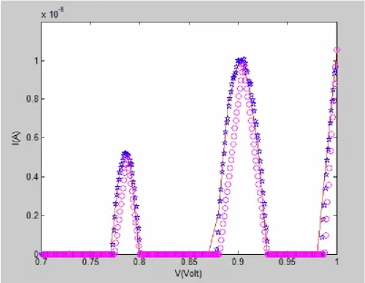
With Rj = 1MΩ, Cj = 0.1aF and T = 0K, simulation results using SIMON, MATLAB,
and the above piece-wise model are shown in Fig 3.5 for comparison, where the
MATLAB results are obtained with input voltage increments of 1mV. It can be seen from
the figure 3.5 that there is a good agreement among these results.
3.3 Impacts of Circuit Parameters and Temperature
The previous discussions are based on the parameters (Cg1 = 5Cj and Cg2 = 15Cj). If
the NDC block is operated with different parameters, its I-V characteristic will change as
well. First of all, both threshold voltages and the static current will decrease as the value
of Cj increases. For instance, simulation results with Cj = 0.2aF vs. 0.1aF are shown in
Fig 3.7 (a). Secondly, if Cg2 rises, more peaks can be expected. An example with Cg2 =
25Cj is shown in Fig 3.7 (b). Third, reducing Cg1 will lead to a remarkable growth of
even-number threshold voltages while keeping the odd-number threshold voltages almost
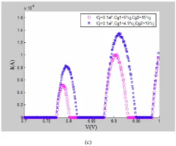
unchanged. Fig 3.7 (c) shows the results with Cg1= 4.9Cj. In general, the specific changes
in the static current and threshold voltages under different parameters can be found.
However, it should be mentioned that the parameter changes are limited by a relatively
small range. Otherwise, the negative slopes of the NDC device may disappear.
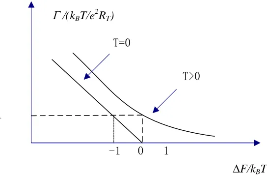
The above discussions assume the ideal temperature T = 0K. As T increases, both the
static current and threshold voltages in the device’s I-V characteristic will be shifted. As
shown in Fig 3.6, with a high temperature, the tunnel rate will not reduce to zero when ∆F
is zero. Since is almost 1 when V1 equal to Vthi, the equation of current can be
expressed as:
I= * (3.16)
1
-1 0 1
T=0
T>0
F/kBT
Г /(kBT/e 2
RT)
Fig 3.6 curves of tunnel rate when T=0 and T>0
The new threshold voltages Vth,i’ under the temperature T can be derived in the same
way as is for Vth,i, except with new tunneling conditions: Vj1 = Vc1 –VT·ln(βT) and Vj2 =
Vc2for i odd, or Vj2 = Vc2 − VT ·ln(βT) and Vj3 = Vc3 − VT·ln(βT) for i even, where VT=
kBT/e, and β is a constant depending on circuit parameters (for the original parameters, β
≈ 4). Thus, the piece-wise model considering temperature effects is expressed as (when
Vth,i’≤ Vth,i+1’for i ≥ 2):
Where Vpeak,i=(Vth,2i-1+Vth,2i)/2 for i = 1, 2, …, k0’ = Ipeak1/(Vpeak1−Vth1’),
k1’=Ipeak1/(Vpeak1−Vth2’), k2’=Ipeak2/(Vpeak2– Vth3’), k3’=Ipeak2/(Vpeak2–Vth4’), …, and Ipeak,i is
given by (5) with V = Vpeak,i.
(c)
Fig 3.7 Simulation results of Fig 3.3 with (a) Cj = 0.2aF, Cg1 = 5Cj and Cg2=15Cj, (b) Cj = 0.1aF, Cg1 = 5Cj and Cg2 = 25Cj, and (c) Cj = 0.1aF, Cg1 = 4.9Cj and Cg2=15Cj, where the circles (purple) and stars (blue) correspond to original parameters (i.e., Cj = 0.1aF, Cg1 = 5Cj and Cg2=15Cj) and new parameters, respectively.
As T keeps increasing, the even-number and odd-number threshold voltages may
overlap, resulting in Vth,i’> Vth,i+1’for i ≥ 2. In this case, (3.17) shall be modified as:
(3.18)
where k0’’=Ipeak1/(Vpeak1−Vth1’), k1’’=(Ipeak1–Ivalley1)/(Vpeak1−Vvalley1),
k2’’=(Ipeak2–Ivalley1)/(Vpeak2–Vvalley1), k3’’=(Ipeak2–Ivalley2)/(Vpeak2-Vvalley2), … , and Ivalley,iis the
(3.19) Or
Vvalley,i = (3.20)
3.4 Simulation Results and Discussion
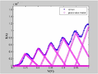
Fig 3.8 shows the simulation results of Fig 3.3 under different temperatures. To further
verify the impacts of circuit parameters on its I-V characteristic under different
temperatures, we also conducted simulations for Fig 3.3 with different parameters and
temperatures. Fig 3.9 shows the results when Cj = 0.1aF, Cg1= 5Cj, Cg2= 35Cj with T =
50K. It can be seen from the figures that the results from the proposed piecewise model
match those from SIMON simulations very well.
(b)
Fig 3.8 Simulation results of Fig 3.3 with Cj = 0.1aF under (a) T = 25K and (b) T = 77K, where the stars (blue) and circles (purple) correspond to SIMON and piece-wise model, respectively.
Chapter 4
Modeling and Application for
Negative-Differential-Conductance Devices with
Single-Electron Technology
NDC elements find many applications in both digital and analog circuits, such as
memory cells and Schmitt triggers. Research shows that single-electron tunneling
technology is especially suitable for NDC block implementations due to the unique
Coulomb oscillations with SET devices.
4.1 Previous Works
4.1.1 G
4-FET Voltage-Controlled NDR Device
The schematic of the conventional, 2-terminal NDR device is shown in Fig 4.1 (a).
The G4-NDR is obtained by replacing the JFETs in Fig 4.1 (a) with complementary
G4-FETs (Fig 4.1 (b)). The resulting structure is a 4-terminal device, the extra 2 terminals
being the front-gate (GI) of the n-channel and p-channel G4-FETs, driven by the voltages
(a)
VN VP
V
G4-NDR
(b)
Fig 4.1 (a) Conventional 2-terminal JFET NDR device (b) Symbol of the 4-terminal G4-NDR
4.1.2 LC Oscillator
As an application example, the G4-NDR loaded with an LC tank constitutes an LC
oscillator (Fig 4.2). The circuit operation is based on the cancellation of the LC circuit
Fig 4.2 schematic of LC oscillator
4.1.3
Schmitt
Trigger
The Schmitt Trigger circuit is obtained by loading the G4-NDR with a regular
inversion-mode PMOS load and connecting the gate of the PMOSFET to the n-type MOS
Fig 4.3 schematic ofSchmitt Trigger
4.2 Multiple-Valued Logic Memory Cells
4.2.1 Schematic Circuit
Multiple-valued logic static memory cell can be designed using two NDCs, as shown
in Fig 4.4 (a) where an extra NMOS switch is used for cell access. The parameters for
both NDCs are: Rj= 1 MΩ, Cj1~j4= Cj = 0.176aF, Cg1= 0.86aF, Cg2= 2.64aF. The power
supply voltage is biased at 1V. The parameters for the NMOS transistor are: W/L =
operates with three logic states: logic “0”, “1” or “2”. For the supply voltage of 1V, these
three logic voltages are approximately 0.44V, 0.5V and 0.56V.
Word line Bit line
NDC2 Load capacitance Supply voltage NDC1 (a)
0 0.2 0.4 0.6 0.8 1
waveform at memory node S
4.2.2 Write Operation for Memory Cell
In Fig 4.4 (a), when both bit line and word line are activated, the input data is written
to the memory node. Once the NMOS switch is OFF, the memory node latches to one of
three logic voltage levels, depending on the written input. Fig 4.4 (b) shows the
simulation results for the write operation. By adjusting parameters and/or supply voltage,
each logic state can be designed to take place near the valley of the NDC’s I-V
characteristics in order to minimize the current required to hold the states.Fig 4.5 shows
three logic states when NDC parameters are: Cj1~j4= Cj =0.176aF, Cg1= 0.86aF, and Cg2=
2.64aF. It should be mentioned that the two extra intersection points (i.e., A and B) in Fig
4.5 are unstable, and thus do not correspond to any logic state. This is due to the fact that
if the voltage (V) at node S increases unexpectedly from VA or VB, the current in NDC2
would be greater than that in NDC1. As a result, the load capacitance CL would be
charged, causing the VA or VB to further increase until it reaches a stable logic state (“1”
or “2”). Similarly, the operating point would leave the point A or B as well if there is a
voltage reduction/disturbance happening at the node S. Therefore, there are only three
stable points in the figure.
4.2.3 Impacts of Circuit Parameters
If NDC blocks are operated with different parameters, their I-V characteristics will
change and the above NDC-based memory cell can operate with different performance
(including the peak-to-valley current ratio, power consumption and noise margin). In Fig
the logic margin of this memory cell, an alternative set of parameters can be used. For
instance, with Cj1= Cj2 = Cj4 = Cj = 0.05aF, Cj3 = 0.35aF, Cg1 = 5.6Cj and Cg2=15.5Cj, the
operating points of the memory are shown in Fig 4.6, where stars/circles and solid curves
represent the I-V characteristics before and after parameter changes, respectively. It can
be seen from this figure that the logic margins are improved significantly to around
200mV, on average, at a cost of more static power.
440 600
400
Voltage(mV)
I
(
A
)
480 520 560
0 0.3 0.6 0.9 1.2
1.5 *10-8
Logic 0
Logic 1
Logic 2
320 800 200 Voltage(mV) I ( A )
440 560 680
0 0.7 1.4 2.1 2.7 3.5 *10-8
Fig 4.6 Impacts of parameters on the memory’s I-V characteristics, where stars/circles correspond to the parameters of Cj1~j4= Cj =0.176aF, Cg1 = 0.86aF and Cg2 = 2.64aF, and solid curves (with improved logic margins) correspond to the parameters of Cj1 = Cj2 = Cj4 = Cj = 0.05aF, Cj3 = 0.35aF, Cg1 = 5.6Cjand Cg2 = 15.5Cj.
4.2.4Temperature Effects
The above discussions assume an ideal temperature T = 0K. As T increases, both the
static current and threshold voltages in the device’s I-V characteristics will be shifted as
well. Both simulations and analytical model show that increasing Cj will reduce both
threshold voltages and the static current. This property can be used for coarse tuning at
high temperatures for a reduced static current. For example, for the parameters in Fig 4.7
(a), there is only one stable point. As Cj increases, two more stable points can be obtained,
as is seen in Fig 4.7 (b). On the other hand, changing Cg1, which only shifts the curves,
will be suitable for fine adjustment, as shown in Fig 4.7 (c) and (d). In addition, for the
logic points.
With an alternative set of parameters, the circuit can also have an improved tolerance
to a higher temperature. For instance, by choosing Cj1 = Cj2 = Cj4 = Cj =0.05aF, Cj3=
0.35aF, Cg1 = 5.6Cj, and Cg2=15.5Cj, the memory cell demonstrates three stable points at
77K, as shown in Fig 4.7 (e). This group parameter (Cj1= Cj2= Cj4= 0.05aF, Cj3=0.28aF)
can actually work even at a temperature of up to 220K, as shown in Fig 4.7 (f).
440 600
400
Voltage(mV)
I(
A)
480 520 560
0 0.3 0.6 0.9 1.2 1.5 *10-8
440 600
400
Voltage(mV)
I(
A)
480 520 560
0 0.2 0.4 0.6 0.8
1 *10-8
(a) (b)
440 600 400 Voltage(mV) I( A)
480 520 560
0 0.2 0.4 0.6 0.8
1 *10-8
Logic 0 Logic 1 Logic 2 Voltage(mV) I ( A ) 0 0.2 0.4 0.6 0.8
1 *10-8
440 600
400 480 520 560
Logic 0
Logic 1
Logic 2
320 800 200
Voltage(mV)
I(
A)
440 560 680
0 0.6 1.2 1.8 2.4
3 *10-8
Logic 1
Logic 0 Logic 2
320 800 200 Voltage(mV) I ( A )
440 560 680
0 0.4 0.8 1.2 1.6
2 *10-8
Logic 2 Logic 0
Logic 1
(e) (f)
Fig 4.7 Simulation results of memory cells with (a) Cj1~j4 = Cj = 0.176aF, Cg1= 0.86aF, Cg2 = 2.64aF at T = 77K, (b) Cj = 0.16aF, Cg1= 0.86aF, Cg2 = 2.64aF at T = 77K, (c) Cj = 0.176aF, Cg1= 0.86aF, Cg2 = 2.64aF at
T = 40K, (d) Cj = 0.176aF, Cg1= 0.9aF, Cg2 = 2.64aF at T = 40K, (e) Cj1 = Cj2 = Cj4 = Cj = 0.05aF, Cj3 = 0.35aF, Cg1 = 5.6Cj, and Cg2 = 15.5Cj at T = 77K, and (f) Cj1 = Cj2 = Cj4 = Cj = 0.03aF, Cj3 = 0.28aF, Cg1 = 5.6Cj and Cg2 = 15.5Cj at T = 220K.
4.3
Schmitt
trigger
The Schmitt trigger circuit is designed by loading a regular PMOS transistor with an
NDC, as shown in Fig 4.8 (a). The parameters for the transistor are: W/L= 0.6μm/0.2μm
with VDD = 1V. Fig 4.8(b) shows its typical voltage transfer characteristic. An important
feature with this NDC-based Schmitt trigger is that its hysteresis window can be adjusted
by using different circuit parameters. Fig 4.9 (a) and (b) show two specific cases
where the window shifts horizontally and vertically, respectively.
In terms of temperature effect, our analytical analysis shows that an ascending
temperature will increase the static current and decrease the Coulomb blockade area,
which makes the hysteresis window smaller and eventually disappear for much higher
temperature. Fig 4.9 (c) shows that the hysteresis window is shrunk almost by half as the
parameters with temperatures of 50K and 100K.
VDD
NDC
Input
Output
(a)
570 586 602 618 634 650
806 837 868 899 930
Voltage(mV)
V
o
l
t
a
g
e
(
m
V
)
775
(b)
75 90 105 120 135 150 240 280 320 360 400 Voltage(mV) V o l t a g e ( m V ) 200 (a)
90 130 170 210 250 290
750 780 810 840 870 900 408 426 444 462 480 Voltage(mV) V o l t a g e ( m V ) 390 (c)
75 90 105 120 135 150
240 280 320 360 400 Voltage(mV) V o l t a g e ( m V ) 200 (d)
Fig 4.9Simulation results of the proposed Schmitt trigger with (a) Cj1 = Cj2 = Cj4 = 0.1aF, Cj3 = 0.7aF, Cg2 = 0.9aF, Cg1 = 0.5aF (solid red curve) or 0.9aF(dotted blue curve), (b) Cj1 = Cj2 = Cj4 = 0.1aF, Cj3= 0.7aF, Cg1 = 0.55aF and Cg2 = 0.9aF (solid red curve) or Cj3= 0.2aF, Cg1= 1.1aF and Cg2= 1.8aF (dotted blue curve), (c) Cj1~j4= 0.2aF, Cg1= 1.0aF, Cg2= 1.8aF at T = 40K (solid blue curve) and 50K (dotted red one), and (d)
4.4 Oscillator Using NDC Inverter
As a high frequency application, the NDC loaded with a P-MOS constructs a
three-stage ring oscillator. The circuit operation is based on the Schmitt trigger circuit
by the four-junction NDC as an inverter (Fig 4. 10(a)). The parameters for the PMOS
are: width =960nm, length =240nm. The supply voltage and load capacitance of each
stage are 2V and 1fF, respectively. The output waveform of the ring oscillator shown
in Fig 4.10 (b), where the oscillation frequency is given by
f = (4.1)
Where N - Number of stages, Td - Delay of the design circuit in seconds
Shifting parameters and increasing temperature will cause change of output
waveform's phase showed in Fig 4.10 (c).These changes are not obviously due to the
static current of NDC block is operated by various parameters in a narrow range.
VDD
NDC 1 Input
NDC 2
NDC 3
Output
Load capacitance 1 Load capacitance 2 Load capacitance 3
(b)
(c)
Chapter 5
An Area-Efficient Ternary Full Adder Using Hybrid
SET-MOS Technology
Full adder is one of the most important arithmetic units for many digital applications.
A highly efficient and effective design for full adder is crucial for high-performance
operation of digital systems. With the single-threshold nature, traditional CMOS devices
have been shown to be less area or power-efficient for designing an MVL full adder or
ternary full adder in this particular case. With ultra-low power consumption and
nanometer size, single-electron transistors with their unique multi-threshold
characteristics are instead a promising alternative. The main problems with SET devices
are the low current drivability and reliability. Thus, an appropriate and natural solution is
to use a hybrid SET-MOS circuit design, having the best of both worlds.
5.1
PREVIOUS WORKS5.1.1 TFA based on CNTFET
In recent literature, Carbon nanotube field effect transistors (CNTFET) are utilized for
the new design methodology which is highly appropriate for MVL logic. Its various
properties, such as low-off current, unique 1-D band structure, are the attractive
features for circuit designers. And P and N type CNTFET have same size and mobility,
main drawback of this circuit is that it utilizes a larger number of transistors [2] [12]
[13] [14]. Figure 5.1 shows schematic diagram of Proposed CNTFET-based TFA cell.
5.1.2 TFA using the Ternary Adiabatic Logic (TAL)
Another logic which can be used for full adder circuit is Adiabatic Logic that
attempts to reduce the power consumption of a circuit by operating it both slowly and
reversibly. A number of Adiabatic Logic families have been proposed. They are
including 2N2P, PAL, CAL, TSEL, and SCAL. The binary logic has been dominated
majority of adiabatic logic families, but Ternary Adiabatic Logic can be considered to
be the ternary derivative for binary Adiabatic Logic [12].
5.2 SET-MOS Literal Gate
Research shows that literal gates are a fundamental block to build an MVL system.
Conventional literal gates are complex and hard to design. However, when implemented
using SET-MOS technology, a literal gate can be constructed in a compact structure using
an NMOS transistor and a SET transistor. Fig 5.2 shows the basic architecture of a
SET-MOS literal gate, where a periodic oscillating of output voltage is realized by
applying a drain voltage of the SET transistor to the gate terminal of a current-biased
MOSFET. The width and height of the output voltage waveform can be adjusted by the
parameters of Fig 5.2, one can implement some basic ternary logic functions. In particular,
a literal gate that produces logic “1” at the output if and only if the input is logic “i ”(i = 0,
1 or 2) is denoted by Xi (refer to Fig 5.2 (b)).
V
in
V
gs2
V
out
I
bais
I
c
(a)
X
i
V
in
V
out
(b)
Fig 5.1 (a) A SET-MOS literal gate, and (b) its circuit symbol where Vout = “1” if and only if Vin = “i” (i = 0, 1, or 2).
5.3
T-Gate
important building block for MVL design since it can be utilized to implement a variety
of logic functions. The schematic of a SET-MOS based T-gate and its circuit symbol are
shown in Fig 5.2, where Xi (i = 0, 1, or 2) is a literal gate, X is the input signal, and Vxi is a
specific ternary logic value depending on the required logic function. Examples of ternary
functions that can be implemented by the T-gate are shown in Table 5.1 For instance, the
successor function is implemented by choosing Vx0 = “1’, Vx1 = “2”, and Vx2 = “0” in
Fig 5.3.
SELECT
(X)
Vx1
Vx2
Vx3
X
0X
1X
2V
outT
0
1
2
X
Vx1
Vx2
Vx3
(b)
Fig 5.2 (a) Schematic of a SET-MOS ternary T-gate, and (b) its circuit symbol, where Vout = Vxi if X = “i ” (i
= 0, 1, or 2)
Table 5.1 Examples of ternary functions using T-gate
Function name Notation Function output for
X = (0, 1, 2)
identity X (0, 1, 2)
complement (2, 1, 0)
successor (1, 2, 0)
5.4 Proposed TFA
The proposed TFA is shown in Fig 5.3, which takes two ternary inputs A and B as well
as a carry-in signal Cin, and generates the sum output SUM and carry-out Cout. The SUM
generator contains T-gates that are controlled by A, B and Cin, while the Cout generator
includes three literal gates plus a binary two-input binary NAND gate and inverter (note:
For this ternary logic, both Cin and Couthave only two possible logic values of 0 and 1). In
this work, the supply voltage (Vdd) is biased at 0.7 V (unless otherwise specified), and the
ternary logic has three voltage levels of 0V (logic “0”), Vdd /2 (logic “1”), and Vdd (logic
0 1 2 A X0 X2 X1 X Y Z B Cin SUM X2 Cin A B Cout 1 1 2 0 2 0 1 0 1 2 0 1 2 0 1 T T T X1 X0
5.5 Simulation Results with Discussions
Simulation was done using Cadence Spectre simulator with 180nnm CMOS model and
SET MIB macro mode to estimate the performance of the proposed TFA under various
conditions. The results of recently published CNTFET-based TFA cells were also taken
for performance comparison. The power supply voltage of 0.7V was used (unless
otherwise stated) throughout our simulations which consider different temperatures and
operating frequencies.
A complete set of input signals (including all 18 possible input combinations) was
applied to the proposed TFA. The performance evaluations were focused on its power,
delay and power-delay product (PDP). The average power consumption is measured as
(5.1)
Where V is the power supply, I (t) is the total current drawn from the power supply, and T
is the simulation time interval.
The PDP is calculated as
PDP = Max (Delay) × Paverage (5.2)
Fig 5.4 shows the simulated results of the proposed TFA, which verifies its correct
operation. Our simulation results also show that the proposed TFA has a lower PDP than
consume more power than other implementations. Fig 5.5 shows part of these results in
comparison with [14] and [16].
The proposed TFA takes advantage of the unique oscillation characteristics of SET
transistors, which contribute to an area-efficient design. This can be seen from Table 5.2
where the transistor counts in different TFA are listed. The proposed TFA needs only 57
transistors, a number much less than all those reported in literature so far.
Simulation results on the temperature effect for the proposed TFA are shown in Fig5.6.
As expected, the power consumption decreases with the rising temperature due to the
performance degradation of MOS transistors. It can also be seen that the delay of TFA
improves as the temperature increases. This is mainly due to the fact that the static current
0 350 0 350 700 700 700 350 350 0 0 0 350 350 V o l t a g e ( m V ) Cin B A SUM Cout
35 70 105 140 180
0
Time(nS)
150
225
300
0
75
30
60
90
120
150
Frequency(MHZ)
Po
we
r(
nW
)
(a)150
225
300
0
75
30
60
90
120
150
Frequency(MHZ)
Po
we
r(
nW
)
(b)TFA Type of transistors # transistors
The proposed SET and CMOS 57
[18] CNTFET 106
[19] CNTFET 142
[20] CNTFET 214
Table 5.2 Comparison of transistor counts required for TFA
7.5
7
6.5
6
De
la
y(
nS
)
10
15
20
25
30
35
Temperature(℃)
170
160
150
140
P
o
w
e
r
(
n
W
)
10
15
20
25
30
35
Temperature(℃)
(b)
Chapter 6
Conclusion and Future Work
6.1 Conclusion
We have presented a piece-wise model for multiple-peak SET-based NDC blocks
with considerations of temperature effects. The model describes the NDC’s I-V
characteristic in terms of input voltage and circuit parameters, making it very useful for
optimization design of NDC application circuits. After the new four-junction NDC block
has been modeled, we applied it to implement multiple-valued memory cell and Schmitt
trigger. With the analytical model, circuit parameters can be adjusted to analyze their
impacts on circuit performance for potential optimization design with different
applications of NDC blocks. Finally, we have proposed a novel design of ternary full
adder based on hybrid SET-MOS technology. By taking advantage of unique Coulomb
oscillations with SET transistors, the proposed circuit structure promises to be more area-
and/or power-efficient than most existing TFA cells. This has been fully supported by
6.2 Future work
The background charge and temperature effect on SET circuit should be solved in the
future. We try to address the reliability issues with the lowest power consumption and
delay.
In chapter 5, we present a novel design of ternary full adder using hybrid
single-electron transistor and MOS technology. More work should be done in reducing
transistor number and optimizing the structure. And a ternary multiplier can be design
References
[1] H. Inokawa, A. Fujiwara, and Y. Takahashi, "A Multiple-Valued Logic and Memory
with Combined Single-Electron and Metal-OxideSemiconductor Transistors," IEEE
Trans. Electron Devices, vol. 50, February 2003.
[2] C. P. Heij, et al., “Negative differential resistance due to single-electronswitching,”
Appl. Phys. Lett., vol. 74, pp. 1042–1044, 1999.
[3] S. Mahapatra and A. M. Ionescu, “A novel single electron SRAM architecture,” Proc.
of IEEE-Nano 2004, vol. 3, pp. 287–289.
[4] K. Akarvardar, et al., “Four-gate transistor voltage-controlled negative differential
resistance device and related circuit applications,” 2006 IEEE International SOI
Conference, pp. 87-88.
[5] B. H. Lee and Y. H. Jeong, “A novel SET/MOSFET hybrid static memory cell
design,” IEEE Trans. Nanotechnology, pp. 377-382, 2004.
[6] N. Syed and C. Chen, “Low-power multiple-valued SRAM logic cells using
single-electron devices,” IEEE International Conference on Nanotechnology, pp.
1174-1177, 2012.
[7] C. Wasshuber, H. Kosina, and S. Selberherr, “SIMON—A simulator for
single-electron tunnel devices and circuits,” IEEE Trans. Computer- Aided Design,
vol. 16, pp. 937–944, Sept. 1997.
[9] K. Likharev, “Single-electron devices and their applications”, Proceedings of the
IEEE, vol. 87, no. 4, April 1999, pp. 606-632.
[10]S. M. Goodnick and J. Bird, “Quantum-effect and single-electron devices,” IEEE
Trans. on Nanotechnology, vol. 2, no. 4, December 2003, pp. 368-385.
[11]H. Suwa. “Geometrically Constructed Markov Chain Monte Carlo Study of Quantum
Spin-Phonon Complex Systems”. 2014, Springer, pp. 11-42.
[12]D. J. Willingham and I. Kale, “A ternary adiabatic logic (TAL) implementation of a
four-bit full adder,” NORCHIP, pp.1-4, 2011.
[13]S. Mahapatra and A. M. Ionescu. Hybrid CMOS single-electron-transistor device and
circuit design. Artech House, 2006.
[14]K. Navi, M. H. Moaiyeri, R. F. Mirzaee, O. Hashemipour, and B. M. Nezhad, “Two
new low-power full adders based on majority-not gates,” Microelectronics Journal of
Elsevier, vol. 40, no. 1, pp.126–130, January 2009.
[15]S. L. Murotiya and A. Gupta, “Design of CNTFET based 2-bit ternary ALU for
nanoelectronics,” International Journal of Electronics, vol. 101, no. 9, pp. 1244-1257,
2014.
[16]S. A. Ebrahimi, P. Keshavarzian, S. Sorouri, and M. Shahsavari, “Low power
CNTFET-based ternary full adder cell for nanoelectronics,” International Journal of
Soft Computing and Engineering, vol. 2, no. 2, pp. 291-295, May 2012.
Heritage Foundation. pp. 67–84. ISBN0-941901-41-6. Retrieved March 15, 2015.
[18]S. A. Ebrahimi, P. Keshavarzian, S. Sorouri, and M. Shahsavari, “Low power
CNTFET-based ternary full adder cell for nanoelectronics,” International Journal of
Soft Computing andEngineering, vol. 2, no. 2, pp. 291-295, May 2012.
[19]K. Sridharan, S. Gurindagunta, and V. Pudi, “Efficient multiternary digit adder design
in CNTFET technology,” IEEE Trans. on Nanotechnology, vol. 12, no. 3, pp.
283-287,May 2013.
[20]S. L. Murotiya and A. Gupta, “Design of CNTFET based 2-bit ternary ALU for
nanoelectronics,” International Journal of Electronics, vol. 101, no. 9, pp.
Appendix A:
Code of four junctions NDC:
MATLAB:
M-file main:
VDS=0:0.01:1;
%VJ=0;0.01;1;
ID1=zeros(1,101);
ID2=zeros(1,101);
for j=1:101
V1=VDS(j);
Icalculate;
ID1(j)=I;
%ID2(102-j)=I
%VJ(j)=Vj2;
end
%plot(VJ,ID,'g')
%hold on
plot(VDS,ID1,'r')
xlabel('V(Volt)')
ylabel('I(A)')
hold on
M-file Icalculate:
e=1.6e-19;
cj=1e-19;
cp=7e-19;
cg1=5*cj;
cg2=15*cj;
c=[cj+cg1 -cj 0 -cg1 0 -cj 2*cj+cg2 -cj 0 -cg2 0 -cj cp+cj -cp 0 -cg1 0 -cp cj+cp+cg1 -cj 0
-cg2 0 -cj cj+cg2];
C1=reshape(c,5,5);
Ce1=cg2+[(cp*cj)/(cp+cj)]*(cj+cg1)/(cg1+[(cp*cj)/(cp+cj)]+cj);
Ce2=(cg1+cj)*cp/(cg1+cj+cp)+(cg2+cj)*cj/(cg2+cj+cj);
Ce3=Ce2;
Ce4=cg1+[(cp*cj)/(cp+cj)]*(cj+cg2)/(cg2+[(cp*cj)/(cp+cj)]+cj);
Vc1=e/2/(cj+Ce1);
![Fig 1.1 a plot of CPU transistor counts [17]](https://thumb-us.123doks.com/thumbv2/123dok_us/1386342.1171321/18.612.148.512.104.378/fig-plot-cpu-transistor-counts.webp)
![Fig 1.2 a plot of new technology generation introductions (1975–2005) [17]](https://thumb-us.123doks.com/thumbv2/123dok_us/1386342.1171321/19.612.124.524.70.328/fig-plot-new-technology-generation-introductions.webp)