Abstract
Kim, Indong.
Device Fabrication and Characterization for
Alternative Gate Stack Devices.
(Under the direction of Dr.
Carlton M. Osburn)
Aggressive scaling has continued to improve MOSFET transistor performance. An effective oxide thickness (EOT) less than 1.0nm is required for future technology nodes. However, tunneling currents of SiO2 become quite prominent below 1.5nm, leading to high leakage current. High-K dielectrics are required to reduce this leakage. A thicker dielectric reduces the probability of electron and/or hole tunneling through the gate dielectric and therefore the tunneling current. The use of metal gate electrodes is one of the technologies assumed in ITRS roadmap to circumvent the high sheet resistance and depletion associated with poly-Si gates.
The objective of this research is the demonstration and evaluation of devices made with high-K dielectrics and metal gate electrodes.
out the high-K dielectric candidates were generated and several candidates were seen to meet the requirements for the most demanding node.
Secondly, NMOS and PMOS devices with alternative gate stacks were fabricated and evaluated using a new non-self aligned process, which reversed the order of junction and gate stack formation. The effect of post metallization annealing and device stability were also evaluated. NMOS and PMOS devices having high-K dielectrics such as HfO2, ZrO2, and La2O3 and metal gate electrodes such as TaN, Pt, Al, and Poly-Si were fabricated and characterized. From the various splits of alternative gate stack devices, PVD HfO2 with an equivalent oxide thickness of 1.2 nm had a channel mobility comparable to SiO2.
The effect of post metallization annealing of devices having PVD HfO2, MBE La2O3 or RPECVD Y2O3 dielectrics and poly-Si or TaN gate electrodes was studied. Forming gas (10% H2 / 90% N2) annealing at 400°C enhanced drive current and channel mobility for devices having 1.2nm HfO2 gate dielectrics by eliminating interface states. Post metal annealing using 10% deuterium for 1.2nm HfO2 gate dielectrics resulted in larger enhancement drive currents and device channel mobility as compared to forming gas anneals. Similar enhancements of the device characteristics were observed in La2O3 (300mV shift in both flatband and threshold voltage) and Y2O3 (200mV shift only in threshold voltage) materials. Annealing in pure nitrogen was found to degrade the dielectric quality of HfO2, including a decrease in device current and 50% lower capacitance.
were measured as a function of stress time and stress current over the range of 10-3 to 105 coulombs of injected charge per square centimeter. With forming gas annealed HfO2, positive shifts in the threshold voltage exhibited a power law dependence on the injected charge (∆Vt ∝ QINJ 0.1). Stressing at high current was seen to generate traps. Stressing at low current levels revealed a saturation of the threshold voltage after modest stressing times. Stressing deuterium annealed samples resulted in less Vt and gm shift (under high injection conditions), which was attributed to the effectiveness of heavier D2 in preventing trap generation under high stressing conditions. Y2O3 stressed at similar electric fields displayed negatively shifted threshold voltages, and the transconductance increased.
Finally, the properties of dilute Hf silicate were studied. A leakage minima was found at an intermediate Hf silicate (45~75% HfO2) composition. Nitirdation inhibited oxygen diffusion through Hf silicate dielectrics, and resulted in lower EOTs (10% lower) for nitrided samples. Also, interface plus surface nitridation effectively removed positive charges in silicates.
Device Fabrication and Characterization for
Alternative Gate Stack Devices
by
Indong Kim
A dissertation submitted to the Graduate Faculty of North Carolina State University
in partial fulfillment of the requirements for the Degree of
Doctor of Philosophy
ELECTRICAL AND COMPUTER ENGINEERING Raleigh, NC
May 2003
APPROVED BY:
Dr. Carlton M. Osburn Dr. John R. Hauser Chair of Advisory Committee
ii
BIOGRAPHY
Indong Kim was born on Feb 7. 1974 in Pu-san, Korea. He is the lastborn to his parents, Jae Han Kim and Kyung Ok Park. He has a sister and a brother. When he was 2 years old, his family moved to the capital of Korea, Seoul, where his father started his own business.
After graduating from Youi-Do high school, he attended Kwangwoon University (Seoul, Korea) where he started his college life in electronic materials engineering. His curiosity in electrical engineering field was inherited from his father, who is also an electrical engineer for his life. He played with many electronics parts when he was young and tried to fix appliances things when they were broken (not always successful though). As he grew up, he became to be more interested in Transistors and IC technology because he became to realize they are the major driving force for him to have more smaller and fancier electronic devices.
After finishing his 1st semester of sophomore year, he joined the army of his service to his mother nation. During 26 months of mentally and physically challenging army service, he had earned valuable experiences and was be able to become a stronger person.
Being discharged, he came to the United States of America to take an English language course at the University of Florida (Gainesville, FL). After taking the intensive English courses, he traveled through Florida, Michigan, New York City and California. During the travel, major universities in those locations were always on his ‘place to visit’ list because he already was becoming interested in studying in United States at that time.
iii
was admitted to North Carolina State University in August 1999, where he met his mentor Dr. Carlton M. Osburn. He joined Dr. Osburn’s SRC/Sematech funded research project and earned M.S. degree in 2001. In year 2001, another great thing happened. He became the husband of Jung-Hee, who has just been waiting and supporting him remotely in Korea during his first and second year of graduate study.
iv
ACKNOWLEDGEMENT
First of all, my sincere gratitude goes to my Ph.D. committee members, Dr. Carlton M. Osburn, Dr. John R. Hauser, Dr. Veena Misra and Dr. Jon-Paul Maria for their support and patience. Special thanks go to Dr. Osburn, who has served as my advisor, my committee chairman and my mentor. Without his help, I would not been able to finish my graduate study. He was always available and gave me an excellent suggestions based on his knowledge, whenever I need either technical or personal advice or help.
My Ph.D. work and all the experiments would not have been successful without help of the staff members of the Microelectronic Laboratory at North Carolina State University. It seems there is no way for me to pay off my dept with Joan O’Sullivan. Also, my sincere gratitude goes to Dr. Donna Ginger Yu, Harold Morton, Henry Taylor and John Todd.
Special thanks to the administrative staff of Advanced Electronics Materials Processing (AEMP)- Ms. Rajani Verghese and Ms. Elizabeth Bell for being supportive throughout my stay in this facility.
v
Jae-Hoon Lee, You-Seok Suh, Huicai Zhong, Zing Liu, Kam F. Yee, Indranil De, Heather Lazar, Dexter Hodge, Dwi Wicaksana, Bill Kiether, Mais Homsi, Shyam Gannavaram, Chad Young, Eric Rying and Greg Heuss.
I also thank the Semiconductor Research Corporation (SRC) and Sematech, for funding research and the research groups in many other Universities (Prof. J. Lee and D.L. Kwong and their students at University of Texas Austin, Prof. T.P. Ma and his students-Wenjuan Zhu and Zhijong Luo, Prof. Campbell and his students at University of Minnesota and Prof. Tsu-Jae King and her students at University of California at Berkeley) within the SRC/Sematech Front End Processing research center.
Personally, I owe lots of things to my friends - Jun Sung, Seung Ho, Kwang Ho, Won Tae, Do Young and Chan Kyu and friends here at NC State - Song Jun Doh, Hyungmin Bae, Dr. Manyoo Han, Dr. Jae-hwan Oh, Dong-wook Jung, Eun Chu Oh, Dr. Eun-Kyung Lee, Jisang Hwang, Jin-Ho Lee, Sung Won Ha, Young Joon Cho, Eun Kyung Cho, Woo Young Choi, and Hyun-Jik Lee. I will never forget the precious time I spent with them and the moral support they gave me. And many thanks to David Holcombe for proofreading of this thesis.
vi
my study. I must specially thank to my father for his belief in my academic achievement and mental support during my academic journey. My parents worked long and hard hours in years just for one hope-brighter future for their children. I really appreciate that.
vii
TABLE OF CONTENTS
List of Figures……….…..ix
List of Tables………...xiii
Chapter 1: Introduction 1.1. Introduction….………...…....….…………..1
1.2. Issues with gate oxide scaling……….………..……….……….…..1
1.3. High-K Gate Dielectrics……….……….………...4
1.4. Metal Gate Electrode……….………..………...………..5
1.5. Overview of Dissertation……….………...………….……….7
Chapter 1 References………...……….8
Chapter 2: Gate Leakage Requirements for Future ITRS Nodes 2.1. Introduction……….…...……….14
2.2. Gate Leakage Current for Alternative Gate Stack Devices………..……….….14
2.3. Gate Leakage Requirement for Future ITRS Nodes……….………….……….16
2.3.1. Simulation Study of the Gate Leakage for Future ITRS Nodes………...16
2.3.2. The Tradeoff between Dielectric Constant, K, and Band Offset, φn………....17
2.3.3. Validation of UTQUANT with PVD HfO2………..19
2.4. Conclusions………...………..20
Chapter 2 References………...………...21
Chapter 3: Device Fabrication and Evaluation of Alternative High-K Dielectrics and Gate Electrodes Using a Non-Self Aligned Gate Process 3.1. Introduction………...………..36
3.2. Device Fabrication………..………36
3.3. Results and Discussions………...………...38
3.3.1.Capacitance Voltage (CV) and Gate Leakage (Ig-Vg)………….………..38
3.3.2. Device Characteristics………..………40
3.3.3. Mobility Analysis………..………...41
3.4. Conclusions………..………….…..42
Chapter 3 References………...………...44
Chapter 4: Effect of Post Metallization Annealing for Alternative Gate Stack Devices 4.1. Introduction………..………..73
4.2. Experiment………..……...73
4.3. Results and Discussion………...75
4.3.1. The Effect of the 10% Hydrogen Forming Gas on PVD HfO2 with n+ Poly-Si Devices……….…………..………75
viii
4.3.4. The Effect of the 10% Hydrogen Forming Gas on
MBE La2O3 and MOCVD Y2O3 with TaN and Poly-Si gate Devices…..…...77
4.4. Conclusions……….78
Chapter 4 References………...………...80
Chapter 5: Stability of Advanced Gate Stack Devices 5.1. Introduction………...………104
5.2. Experiment………...……….105
5.2.1. Device Fabrication………..………105
5.2.2. Device Stability Evaluation…..………..105
5.3. Results and Discussion………..………...106
5.3.1. Stability of PVD HfO2 with n+ Poly-Si Device Properties and the Modeling of the Parameter Changes………..………106
5.3.1.2. Threshold Voltage Recovery………...109
5.3.1.3. Change in Gate Leakage Current during Stressing (SILC)……….110
5.3.2. Stability of RPECVD Y2O3 with n+ Poly-Si Devices………110
5.4. Conclusions………...111
Chapter 5 References………...……….113
Chapter 6: Device Fabrication and Characteristics of Hf Silicate with Poly-silicon and Metal Gate Electrodes 6.1. Introduction………...136
6.2. Experiment……...……….137
6.3. Results and Discussions………...……….138
6.3.1. Leakage Characteristics of Hf Silicate Alloys for Different Compositions...138
6.3.2. Effect of Nitridation………...……….139
6.3.3. Thermal/Chemical Effects on Hf Silicate Gate Dielectrics………140
6.4. Conclusions………...141
Chapter 6 References………...……….142
Chapter 7: Summary and Conclusions 7.1. Conclusions………...162
7.2. Gate Leakage Requirements for Future ITRS Nodes………...…162
7.3. Device Fabrication and Evaluation of Alternative High-K Dielectrics and Gate Electrodes Using a Non-Self Aligned Gate Process….……….163
7.4. Effect of Post Metallization Annealing for Alternative Gate Stack Devices………163
7.5. Stability of Advanced Gate Stack Devices………...164
7.6. Device Fabrication and Characteristics of Hf Silicate with Poly-silicon and Metal Gate Electrodes………165
ix
LIST OF FIGURES
Fig. 2.1 Band diagram of tunneling mechanisms.
(a) Direct tunneling (b) Fowler-Nordheim tunneling……….28
Fig. 2.2 (a) Direct tunneling through entire stack………..…….…………..29
Fig. 2.2 (b) Fowler Nordheim tunneling………...29
Fig. 2.2 (c) Direct tunneling through one layer into the conduction band of next layer…29 Fig. 2.3 The comparison of UTQUANT simulation of SiO2 leakage current with Lo model …….………30
Fig. 2.4 Simulated versus specified gate leakage of SiO2 for different ITRS nodes.…...31
Fig. 2.5 Measured gate leakage currents for three oxynitride films as compared to the data for three thermal SiO2 films of similar thicknesses…...……….…...32
Fig. 2.6 The leakage current of oxynitride for varied nitride composition……….…..…33
Fig. 2.7 UTQUANT Simulation for PVD HfO2 gate dielectrics……….….34
Fig. 2.8 Trade off between dielectric constant and band offset for low standby power 22nm node………...………35
Fig. 3.1 Schematic illustration of non-self aligned gate process………..52
Fig. 3.2 C-V curves of JVD HfO2. Al samples received 600˚C 20min FG post-deposition anneal, while Pt samples got 600˚C, 20min N2 annealing....….53
Fig. 3.3 C-V curves of ZrO2 with different metal gates. RTCVD samples received, 900°C, 30sec N2 annealing while JVD samples got 550°C, 20min FG post-deposition annealing…………54
Fig. 3.4 Effect of PMA on TaN gates………...55
Fig. 3.5 I-V curves of HfO2 with different metal gate electrodes...………..56
Fig. 3.6 I-V curves of ZrO2 with different metal gate electrodes ……..………..57
Fig. 3.7 (a) NMOS, subthreshold characteristics of HfO2 devices………58
Fig. 3.7 (b) PMOS subthreshold characteristics of HfO2 device………...59
Fig. 3.8 (a) NMOS, subthreshold characteristics of ZrO2 devices……….60
Fig. 3.8 (b) PMOS subthreshold characteristics of ZrO2 device………61
Fig. 3.9 Subthreshold characteristics of La2O3(NCSU) NMOS device………62
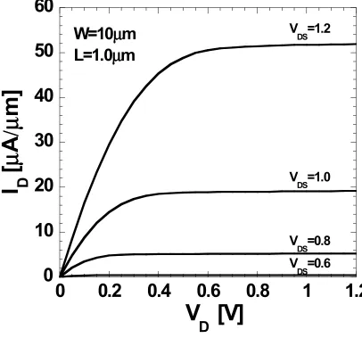
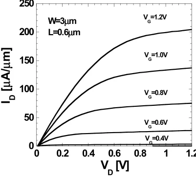
Fig. 3.10 Id-Vd characteristics of HfO2(JVD)-Al device………..63
Fig. 3.11 Id-Vd characteristics of HfO2 (RTCVD)-Poly NMOS device…….…………...64
Fig. 3.12 Id-Vd characteristics of ZrO2(JVD)-TaN device………...65
Fig. 3.13 Id-Vd characteristics of ZrO2(JVD)-Al NMOS device………..66
Fig. 3.14 Id-Vd characteristics of La2O3-TaN NMOS device………....67
Fig. 3.15 Id-Vd characteristics of HfO2(JVD)-Pt PMOS device………68
Fig. 3.16 Id-Vd characteristics of ZrO2 (JVD)-Pt PMOS device……….……..68
Fig. 3.17 Extracted NMOS mobility……….……70
Fig. 3.18 Extracted PMOS mobility………….………71
Fig. 3.19 Reliability of HfO2………72
x
electrode; (d) Pattern and etch gate electrode/gate dielectric, and deposit and pattern contact metal……….………..……83 Fig. 4.2 Jg-Vg characteristics for 1.2nm HfO2 with poly gate MOSCAPs…...….….…...84 Fig. 4.3 C-Vg characteristics for 1.2nm HfO2 with poly gate MOSCAPs……….……...85 Fig. 4.4 Id-Vg characteristics for 1.2nm HfO2 with poly MOSFETs……….…...…86 Fig. 4.5 MOSFET mobility characteristics for 1.2nm HfO2 MOSFETs………..87 Fig. 4.6 Quasi-static C-Vg characteristics of 1.2nm HfO2………....…88 Fig. 4.7 Weibull distribution of threshold voltages of 1.2nm HfO2 MOSFETs…….…..89 Fig. 4.8 (a) C-Vg characteristics for 1.2nm HfO2 with poly gate MOSCAPs
with D2 annealing……...………..………....90 Fig. 4.8 (b) C-Vg characteristics for 1.2nm HfO2 with poly gate MOSCAPs
with D2 annealing…...………..………91 Fig. 4.9 Id-Vg characteristics for 1.2nm HfO2 with poly gate MOSCAPs
with D2 annealing, in comparison with H2 annealing...………...92 Fig. 4.10 MOSFET mobility characteristics for HfO2 MOSFETs
with D2 annealing, in comparison with H2 annealing…...……….…...93 Fig. 4.11 Id-Vg characteristics for 1.2nm HfO2 with poly MOSFETs
before and after N2 anneal...………...……..……….94 Fig. 4.12 C-Vg characteristics for 1.2nm HfO2 with poly gate MOSCAPs
before and after N2 anneal………...………..………95 Fig. 4.13 MOSFET mobility characteristics for 1.2nm HfO2 MOSFETs
before and after N2 anneal……….96 Fig. 4.14 C-Vg characteristics for 5nm La2O3
with TaN gate MOSCAPs………..…………...97 Fig. 4.15 C-Vg characteristics for 3.1nm Y2O3
with poly gate MOSCAPs……….98 Fig. 4.16 Jg-Vg voltage characteristics for 5nm La2O3
with TaN gate MOSCAPs………...…..99 Fig. 4.17 Id-Vg characteristics for 5nm La2O3
with TaN gate MOSFETs……….………...100 Fig. 4.18 Id-Vg characteristics for 3.1nm Y2O3
with poly gate MOSFETs………...…………101 Fig. 4.19 Mobility characteristics for 5nm La2O3
with TaN gate MOSFETs………...………102 Fig. 4.20 Mobility characteristics for 3.1nm Y2O3
with poly gate MOSFETs……….……..103
Fig. 5.1 (a) Capacitance vs. Gate Voltage characteristics of 1.2nm HfO2
with poly-Si gate capacitor………...………...116 Fig. 5.1 (b) Leakage Current vs. Gate Voltage characteristics of 1.2nm HfO2
with poly-Si gate capacitor ……….………..………..117 Fig. 5.1 (c) Drain Current vs. Gate Voltage characteristics of 1.2nm HfO2
xi
with poly-Si gate nMOS devices after 0.8 and 8A/cm2 stressing ………119 Fig. 5.3 (a) Device current of 1.2nm HfO2 with poly-Si gate nMOS devices
under 0.8A/cm2 stressing ………120 Fig. 5.3 (b) Mobility of 1.2nm HfO2 with poly-Si gate nMOS devices
under 0.8A/cm2 stressing .…...………121 Fig. 5.4 Interface scattering and roughness of 1.2nm HfO2
with poly-Si gate nMOS devices after 0.8 and 8A/cm2 stressing ………122 Fig. 5.5 (a) Threshold voltage and transconductance shift of 1.2nm HfO2
with poly-Si gate nMOS devices after 80, 8 and 0.8mA/cm2 stressing...…123 Fig. 5.5 (b) Threshold shift and the injected charge at the onset of saturation
for different stress current …..……….124 Fig. 5.6 (a) Drain current vs. gate voltage characteristics of HfO2
with poly gate device under 8mA/cm2 stressing ….………...……….125 Fig. 5.6 (b) Mobility parameters of 1.2nm HfO2 with poly-Si gate nMOS devices
after 8mA/cm2 stressing ………..126 Fig. 5.7 (a) Comparison of threshold voltage shift of 1.2nm HfO2
with poly-Si gate nMOS devices after H2 and D2 annealing ………..127 Fig. 5.7(b) Comparison of transconductance shift of 1.2nm HfO2
with poly- Si gate nMOS devices after H2 and D2 annealing ……...……...128 Fig. 5.8 Threshold voltage shift of 1.2nm HfO2 with poly-Si gate nMOS devices
after 0.008, 0.8 and 0.8A/cm2 stressing ………...129 Fig. 5.9 Threshold voltage and transconductance shift of 1.2nm HfO2
with poly-Si gate nMOS devices after 0.8A/cm2
followed by zero stress measurement to monitor recovery………..130 Fig. 5.10 Change in gate leakage current of 1.2nm HfO2
with poly-Si gate nMOS devices after 0.8A/cm2 stressing……….…131 Fig. 5.11 (a) Capacitance vs. Gate Voltage characteristics of 3.1nm Y2O3
with poly-Si gate nMOS capacitor……..………...132 Fig. 5.11 (b) Leakage Current vs. Gate Voltage characteristics of 3.1nm Y2O3
with poly-Si gate nMOS capacitor………....….133 Fig. 5.11 (c) Drain Current vs. Gate Voltage characteristics of 3.1nm Y2O3
with poly-Si gate nMOS device………...……….134 Fig. 5.12 Threshold voltage and transconductance shift of 1.17nm Y2O3
with poly-Si gate nMOS devices under 1.2V stressing………..……135
Fig. 6.1 (a) Gate leakage current ( corrected for 1 nm EOT)
at -1V gate bias for different silicate composition……….…………..146 Fig. 6.1 (b) Thickness dependence of the leakage current of SiO2 and HfO2………….147 Fig. 6.2 (a) C-V characteristics of Hf silicate/poly-silicon gate stack
with different nitridation conditions………...148 Fig. 6.2 (b) C-V characteristics of Hf silicate/Al gate stack
with different nitridation conditions...……….149 Fig. 6.3 (a) Interfacial and surface nitridation effect on EOT
xii
(Hf silicate with Al gate)….……….151 Fig. 6.4 (a) Interfacial and surface nitridation effect on EOT
(Hf silicate with poly-silicon gate)………..152 Fig. 6.4 (b) Interfacial and surface nitridation effect on flat band volgates
(Hf silicate with poly-silicon gate)………..153 Fig. 6.5 C-V Characteristics of Al gated Hf silicate capacitors
with four different temperatures (600 ºC, 800 ºC, 900 ºC, and 1000 ºC)…….154 Fig. 6.6 Ig-Vg characteristics of MOCVD Hf silicate
with Al metal gate………...………..155 Fig. 6.7 C-V characteristics of three different silicon gates
(LPCVD poly-silicon, LPCVD amorphous silicon,
and PVD amorphous silicon)………156 Fig. 6.8 (a) Gate leakage characteristics of 550°C LPCVD amorphous-silicon……….157 Fig. 6.8 (b) Gate leakage characteristics of 625°C LPCVD amorphous-silicon…...….158 Fig. 6.8 (c) Gate leakage characteristics of PVD amorphous silicon…...………..159 Fig. 6.9 C-V characteristics of two different
(Al and TaSixNy) metal gates………...………..160 Fig. 6.10 Gate leakage characteristics of two different
xiii
LIST OF TABLES
Table 2.1 Expressions for various tunneling mechanisms……….………...25
Table 2.2 2001 ITRS requirements for EOT, Vdd and Jg. 3 data sets for each column; high performance, low operating power and low standby power application (from the left)………...………..………..26
Table 2.3 Material properties of high-K candidates……….27
Table 3.1a Deposition methods for high-K dielectrics……….…………47
Table 3.1b Deposition methods for gate electrodes……….……….48
Table 3.2 Etching recipe for different gate electrode and dielectric materials….………49
Table 3.4 Equivalent oxide thickness (EOT) of each dielectric as extracted from mobility and C-V measurements (nm).….……….50
Table 4.1 Splits of the gate electrodes and dielectrics……….……….82
Table 5.1 10-Year Projection of Vt Shifts for Each ITRS Node………....115
1
Chapter 1
Introduction
1.1. Introduction
Since the disclosure of the basic concepts underlying the MOSFET (Metal-Oxide-Semiconductor Field Effect Transistor) operation, the pace of growth of MOS technology in both R&D and industrial sectors has exceeded any projections that were made. As the
device dimensions have decreased to sub-micron and deep sub-micron levels, the processes and materials have been pushed to their limits; thus, innovative materials, device ideas and alternate process techniques have become increasingly important to
keep up with the International Technology Roadmap for Semiconductors (ITRS) projections [1-4].
The ITRS assumes many new technologies such as: high-K gate dielectrics, metal gate electrodes, low contact resistivity materials, a single drain device structure, etc. It cannot be assumed that all these new materials will be able to withstand the thermal and
chemical processing conditions of the current CMOS technology. Most of the proposed device structures with new materials use conventional processing approaches and hence
suffer from the similar thermal limitations as normal MOSFETs do.
This chapter will describe why high-K dielectrics and metal gate electrodes are currently needed and what kinds of properties are required for these materials.
1.2. Issues with gate oxide scaling
2
years for the following three primary reasons: (a) it passivates the silicon surface and p-n
junctions intersecting the surface, with a low surface-state density (=1~3×10¹⁰/eV-cm2) (b) it serves as a patternable mask, forming a blocking, amorphous layer, for the localized diffusion of commonly utilized dopants in silicon for p-n junction fabrication; (c) it is an
insulator, with a large energy gap (≅9eV), and affords a convenient material for
deposition of adherent, conducting films connecting the various device components in the IC, separating the metallic conductor films from silicon.
According to the 2001 ITRS [4] the thicknesses of the SiO2 layer required for the 45
and 70 nm technology nodes for low-operating power logic are 1.0nm and 1.3nm, respectively. Tunneling currents become quite prominent below 1.5nm leading to high
leakage current [5-7]. The electric field is inversely related to the thickness of the dielectric layer; for dielectrics with higher K than SiO2, the thickness equivalent to that of
oxide would be higher by the factor KDIELECTRIC/KOXIDE. For the same band offset, a
thicker dielectric reduces the probability of electrons and/or holes tunneling through the gate dielectric and therefore the tunneling current. When the direct tunneling gate leakage
current for SiO2 films is comparable to the NMOSFET off-current, the off-state power
level of the circuit is increased. As the oxide thickness scales down below 1.5nm, the direct tunneling gate-to-channel leakage current for SiO2 increases exponentially with
decreasing oxide thickness. In the thin oxide regime, a 0.1nm decrease in SiO2 thickness
results in about a one-half order of magnitude increase in gate leakage current density.
Even though transistors can still function where igate and ioff are comparable, the power
3
allowable stand-by power consumption. Alternative gate dielectrics with high-K have
been proposed to obviate the power concern.
Quantum mechanical quantization and polysilicon depletion effects are also aggravated due to the use of thinner oxide. Both quantum mechanical quantization and
polysilicon depletion effectively increase the separation of the gate and the inversion charge. This results in reduction in the control of channel inversion charge by the gate
electrode and thus can be interpreted as an increase in oxide thickness.
Another important issue related to the thin SiO2 layer is dopant penetration through
the gate oxide, especially boron diffusion out of p+ polysilicon gate, which is a major
problem in scaled MOSFET devices. Dopant penetration increases the threshold voltage and decreases the mobility of the carriers in the channel.
From the processing point of view, it is difficult to grow a uniform ultra thin oxide layer e.g. 0.9nm of SiO2, which is only 3 monolayers thick. Furthermore it is very
difficult to achieve a perfect stoichiometry for such a thin layer. Non-uniform dielectrics
can also further enhance the tunneling current through the gate oxide and provide a rough interface. Considering the issues related with the decrease in the thickness of SiO2 layer
as the gate dielectric, the alternative is to look into high-K dielectrics. The major advantage of going to high-K material is the increase in the thickness of the dielectric layer. Prior to the use of high-K dielectrics, successful incorporation of oxide/nitride gate
4
1.0~1.5nm regime. For sub 100nm technology nodes, new high-K dielectrics are
required. The use of an alternative dielectric material is intended to improve all the electrical properties discussed above. Unlike SiO2, which can be thermally grown over
the channel, high-K dielectrics have to be deposited.
1.3. High-K Gate Dielectrics
To be an acceptable high-K gate dielectric for advanced MOSFETs, the dielectric must a) have a high tunneling barrier height to both electrons and holes, b) have a high dielectric constant, c) form a stable interface with Si as well as gate electrode (low
interface state density), d) have a low fixed charge and smooth surface with a high channel mobility. A few candidates with dielectric constants of 10~80 such as Ta2O5
[8-10], TiO2/Si3N4 [11], TiO2 [12], and SrTiO3 [13] have been reviewed, but low thermal
stability was a major problem.
Recently, Group IVA (Hf and Zr) metal oxides have received significant attention as
alternative gate dielectrics due to their thermodynamic stability, low interface states on Si and large barrier height [14]. An ultra thin HfO2 gate dielectric (EOT = 9~12.3Å) with Pt
and n+ polysilicon gate has been achieved [15,16], and it has a dielectric constant of ~28. The equivalent oxide thickness (EOT) of film was stable up to 700 ºC. With polysilicon gates, HfO2 films remained high quality even after the high temperature dopant activation
step. Hobbs, et al. successfully demonstrated 80nm Poly-Si gate CMOS [17]. ZrO2 films
5
Crystallization of both Hf and Zr oxides has been shown [18, 19] and their silicates
can phase separate [20] at junction formation temperature, which may range from 1~100
seconds at 950°C~1050°C. Several techniques have been suggested to obviate the
thermal stability problem of the high-K dielectrics including silicate formation [21~25] and nitridation of the films [26~33].
La2O3 and Y2O3 have also been considered as alternative gate dielectric candidate due
to their relatively better thermodynamic stability on Si and higher dielectric constant [34].
But silicate formation of these films is still problematic, which reduces the dielectric constant and consequently degrades device properties.
Substantial research and significant results have been shown in the field of high-K
dielectric constant over the past several years. Despite these improvements, a clear winner has not been declared for a gate dielectric replacement for SiO2.
1.4. Metal Gate Electrode
The need for the metal gate electrodes arises from the limitations of present
polysilicon-gate technology. Some of the limitations of the poly-Si gates are
(a) Sheet resistance: the sheet resistance of poly-Si is much higher than that of metal
ones.
(b) Dopant penetration: The poly-Si has to be externally doped with impurities (dopants). During the doping thermal cycle, it is difficult to avoid penetration of
6
(c) Poly depletion: Modern CMOS processing requires the use of n+ poly-Si gates for
NMOS and p+ poly-Si gates for PMOS, and this is normally accomplished by ion implantation and subsequent annealing. But, since ultra shallow junctions are required for deep sub-micron devices, the energy of implantation and the dopant
activation temperature have been reduced substantially which result in lower doping of the poly-Si gate, especially at the oxide-Poly Si interface. The reduction
in dopants at the interface of oxide and poly-Si leads to a depletion layer in the gate and an increase of the effective oxide thickness. Therefore the threshold voltage increases and transconductance decreases [35]. These results directly
translate into a decrease in the drive current. The poly-Si depletion becomes more severe as the effective dielectric thickness is reduced.
Replacing the polysilicon gate electrodes with metal gate electrodes imposes serious manufacturing and reliability challenges. Thermal/chemical stability and process compatibility with high-K dielectrics as well as compatibility with the current CMOS
processing is required. Dual metal gate electrodes should have appropriate metal work functions for NMOS and for PMOS. For conventional device operation, the optimum
work functions are within 0.2 eV of the conduction and valance band edges of Si [36].
Work functions have been measured for different metals (Ta, TaN, Ti, TiN, Ru, RuO2, Hf,
HfN, Zr, Al) by evaluating the flat band voltages on SiO2, ZrO2 and ZrSiO4 [36]. The
work functions of Ta, TaN, Ti, Hf and Zr were found to be near the conduction band of Si while those of Pt and RuO2 were near the valance band, making these materials
7
1.5. Overview of Dissertation
This research focuses on device fabrication and characterization of alternative gate stack devices. An in-depth discussion on device characterization and parameter extraction is provided in Chapter 2. A projection of the requirements for high-K dielectrics for
future technology nodes is given in Chapter 2 using a design of experiment (DOE) method. In Chapter 3, various high-K gate dielectric and metal gate electrode candidates
are evaluated using gate last process. Analyses on device characteristics, including the effect of the post-metallization annealing and device stability is given later (Chapter 4 and 5), and are focused on the most-promising gate materials based on the evaluation
8 Chapter 1 References
[1] G.E. Moore, “Cramming More Components Onto Integrated Circuits,” Electronics,
Vol. 38, No.8, 114 (1965)
[2] G.E. Moore, “Progress in Digital Integrated Electronics,” IEDM Tech. Dig., Vol. 11
(1975)
[3] G.E. Moore, “Lithography and The Future of Moore’s Law,” SPIE, Vol. 2438, p.2
(1995)
[4] International Technology Roadmap for Semiconductors (ITRS), 2001 Edition, Dec.,
2001, Semiconductor Industry Association (2001)
[5] K.F. Shduegraf, C.C. King, and C. Hu, “Ultra-thin Silicon Dioxide Leakage Current
and Scaling Limit,” Symp. On VLSI Tech. Dig., p. 18 (1992)
[6] S-H. Lo, D.A. Buchanan, Y. Taur and W. Wang, “Quantum-Mechanical Modeling of
Electron Tunneling Current from the Inversion Layer of Ultra-Thin-Oxide nMOSFET’s,”
IEEE Elec. Dev. Lett., Vol. 18, No. 5, p.209 (1997)
[7] P. Zeitzoff, “Front-End Trends, Challenges, and Potential Solutions for The 180 –
100 nm IC Technology Generations,” Semiconductor Fabtech, 10th edition, p. 275 (1999) [8] Y. Momiyama, H. Minakata, and T. Sugii, “Ultra-Thin Ta2O5/SiO2 Gate Insulator
with TiN Gate Technology for 0.1 mm MOSFETs,” Symp. On VLSI Tech. Dig., p.135
(1997)
[9] D. Park, Y-C. King, Q. Lu, T-J. King, C. Hu, A. Kalnitsky, S-P. Tay, and C-C.
Cheng, “Transistor Characteristics with Ta2O5 Gate Dielectrics,” IEEE Elec. Dev. Lett.,
9
[10] H.F. Luan, S.J. Lee, C.H. Lee, S.C. Song, Y.L. Mao, Y. Senzaki, D. Robert, and
D.L. Kwong, “High Quality Ta2O5 Gate Dielectrcis with Tox,eq<10Å,” IEDM Tech. Dig.,
p.609 (1998)
[11] X. Guo, T.P. Ma, T. Tamagawa, and B.L. Halpern, “High Quality Ultra-Thin
TiO2/Si3N4 Gate Dielectric for Giga Scale MOS Technology,” IEDM Tech. Dig., p.377
(1998)
[12] S.A. Campbell, D.C. Gilmer, X-C. Wang, M-T. Hsieh, H-S. Kim, W. L. Gladfelter,
and J. Yan, “MOSFET Transistors Fabricated with High Permitivity TiO2 Dielectrics,”
IEEE Trans. Elec. Dev., Vol. 44, p. 104 (1997)
[13] R.A. McKee, F.J. Walker, and M.F. Chisholm, “Crystalline Oxdies on Silicon: The
First Five Monolayers,” Phys. Rev. Lett. Vol. 81, p. 3014 (1998)
[14] G.D. Wilk, and R.M. Wallace, “Electrical Properties of Hafnium Silicate Gate
Dielectrics Deposited Directly on Silicon,” Appl. Phys. Lett. Vol. 74, p.2854 (1998)
[15] B.H. Lee, L.Kang, W.-J. Qi, R. Nieh, Y. Jeon, K. Onishi, and J.C. Lee, “Ultrathin
Hafnium Oxide with Low Leakage and Excellent Reliability for Alternative Gate
Dielectric Application,” IEDM Tech. Dig., p.133 (1999)
[16] S.J. Lee, H.F. Luan, W.P. Bai, C.H. Lee, T.S. Jeon, Y. Senzaki, D. Roberts, and
D.L. Kwong, “High Quality Ultra Thin CVD HfO2 Gate Stack with Poly-Si Gate
Electrode,” IEDM Tech. Dig., p. 31 (2000)
[17] C. Hobbs, H. Tseng, K. Reid, L. Dip, L. Hebert, R. Garcia, R. Hedge, J. Grant, D.
Gilmer, A. Frankie, V. Dhandapani, M. Azrak, L. Praphu, R. Rai, S. Bagchi, J. Conner,
S. Becker, F. Dumbya, B. Nguyen, and P. Tobin, “80nm Poly-Si Gate CMOS with HfO2
10
[18] C.H. Lee H.F. Luan, S.J. Lee, T.S. Jeon, W.P. Bai, Y. Sensaki, D. Roberts and D.L.
Kwong, “MOS Characteristics of RTCVD ZrO2 and Zr Silicate Gate Dielectrics,” IEDM
Tech. Dig., p. 1273 (2000)
[19] W.J. Zhu, T. Tamagawa, M. Gibson, T. Furukawa and T.P. Ma, “Effect of Al
Inclusion in HfO2 on the Physical and Electrical Properties of the Dielectrics,” IEEE
Elec. Dev. Lett., 23(11), (2002)
[20] J-P. Maria, D. Wickaksana, J. Parrette, and A. I. Kingon, “Crystallization in SiO2
-Metal Oxide Alloys,” J. Mater. Sci, May Issue, (2002)
[21] A. Kingon, J.-P. Maria, D. Wicaksana and J. Parrette, “An Annealing Study of
La2O3-SiO2 and ZrO2-SiO2 Gate Dielectrics,” Rapid Thermal and Other Short-Time
Processing Technologies II, ECS Proc., PV 2001-9, p. 221-230 (2001)
[22] C.H. Lee, H.F. Luan, S.J. Lee, T.S. Jeon, W.P. Bai, Y. Sensaki, D. Roberts, and
D.L. Kwong, “MOS Characteristics of Rapid Thermal CVD ZrO2 and Zr Silicate Gate
Dielectrics,” IEDM Tech. Dig., p. 27 (2000)
[23] G.D. Wilk, R.M. Wallace, and J. M. Anthony, “Hafnium and Zirconium Silicates
for Advanced Gate Dielectrics,” J. Appl. Phys., 87, 484-492 (2000)
[24] G.D. Wilk, and R.M. Wallace, “Stable Zirconium Silicate Gate Dielectrics
Deposited Directly on Silicon,” Appl. Phys. Lett., 76, p. 436 (2000)
[25] W.-J. Qi, R. Nieh, E. Dharmarajan, B.H. Lee, Y. Jeon, L. Kang, K. Onishi, and J.C.
Lee, “Ultrathin Zirconium Silicate Film with Good Thermal Stability for Alternative Gate
Dielectric Application,” Appl. Phys. Lett., 77, p. 1704 (2000)
[26] D. Wolfe, K, Flock, R. Therrien, R. Johnson, B. Raynor, L. Gunther, N. Brown, B.
11
Deposition of Zirconium Oxide/ Silicon Oxide Alloy (ZrO2)x/(SiO2)1-x (x ≤ 0.5) Thin
Films for Advanced High-k Gate Dielectrics," ULSI Gate Dielectrics, Symp. Mater. Res.
Soc., p. 343-348 (1999)
[27] R. Nieh, R. Choi, S. Gopalan, K. Onishi, C. S. Kang, H.-J. Cho, S. Krishnan and
J.C. Lee, “Evaluation of Silicon Surface Nitridation Effects on Ultra-Thin ZrO2 Gate
Dielectrics,” Appl. Phys. Lett., 81, p. 1663-1665 (2002)
[28] R. Nieh, K. Onishi, R. Choi, H.-J. Cho, C.S. Kang, S. Gopalan, S. Krishna, and J.C.
Lee, “Performance Effects of Two Nitrogen Incorporation Techniques on TaN/HfO2 and
poly/HfO2 MOSCAP and MOSFET Devices,” Proceedings 1st International Workshop
on Gate Insulator (IWGI) Tokyo, Japan, November 1-2 (2001)
[29] H. Cho, C. Kang, K. Onishi, S. Gopalan, R. Nieh, E. Dharmarajan, and J. Lee,
“Novel Nitrogen Profile Engineering for Improved TaN/ HfO2/Si MOSFET
Performance” IEDM Tech. Dig., p. 655, (2001)
[30] H. Cho, C. Kang, K. Onishi, S. Gopalan, R. Nieh, R. Choi, S. Krishnan and J. Lee,
“Structural and Electrical Properties of HfO2 with Top Nitrogen Incorporated Layer,”
IEEE Elec. Dev. Lett., 23, no. 5, p. 249-251 (2002)
[31] C. Kang, H. Cho, K. Onishi, R. Choi, R. Nieh, S. Gopalan, S. Krishnan, and J. Lee,
“Improved Thermal Stability and Device Performance of Ultra-thin (EOT < 10 Å) Gate
Dielectric MOSFET’s by Using Hafnium Oxynitride (HfOxNy),” IEEE Symp. on VLSI
Tech, (2002)
[32] R. Nieh, R. Choi, S. Gopalan, K. Onishi, C. Kang, H. Cho, S. Krishnan and J. Lee,
“Evaluation of Silicon Surface Nitridation Effects on Ultra-thin ZrO2 Gate Dielectrics,”
12
[33] J. Lee, “Nitrogen Incorporation and High-Temperature Forming Gas Anneal for
High-K Gate Dielectrics,” to be published in 202nd Meeting of The Electrochemical
Society, October 20-25, (2002)
[34] A. Chin, Y.H. Wu, S.B. Chen, C.C. Liao, and W.J. Chen, “High Quality La2O3 and
Al2O3 Gate Dielectrics with Equivalent Oxide Thickness 5-10 Å,” Symp. On VLSI Tech.
Dig., p.16 (2000)
[35] C.Y. Wong, J.Y.Sun, Y. Taur, C.S. Oh, R. Angelucci, and B. Davari, “Doping of N+ and P+ Polysilicon in a Dual-Gate CMOS Process,” IEDM Tech. Dig., p.238 (1988) [36] V. Misra, G. Heuss, and H. Zhong, “Advanced Metal Electrodes for High-K
Dielectrics,” MRS Workshop, New Orleans, LI, June 1-2, p.5 (2000)
[37] Y-S. Suh, G.P. Heuss and V. Misra, “Electrical Characteristics of TaSixNy/SiO2/Si
Structures by Fowler-Nordheim Current Analysis,” Appl. Phys. Lett., 80, no.8 (2001)
[38] A. Chatterjee, R.A. Chapman, G. Dixit and I.C. Chen, “Sub-100nm Gate Length
Metal Gate NMOS Transistors Fabricated by Replacement Gate Process,” IEDM Tech.
Dig., p.821 (1997)
[39] W. Zhu, T. Tamagawa, X.W. Wang, B. Halpern and T.P. Ma, “Electrical Properties
of Ultra-Thin Hafnium Oxide Gate Dielectrics,” Semiconductor Interface Specialist
Conference Proceedings, Section 1.2 (2001)
[40] Yanjun Ma, Yoshi Ono, Lisa Stecker, David R. Evans, and S.T. Hsu, “Zirconium
Oxide Based Gate Dielectrics with EOT of Less Than 1.0nm and Performance of
Submicron MOSFET using a Nitride Gate,” IEDM Tech. Dig., p.149 (1999)
[41] Y. H. Wu, M.Y. Yang, and C.M. Kwei, “Electrical Characteristics of High Quality
13
[42] Howard R. Huff, “The Gate Stack/Shallow Junction Challenge for sub-100nm
Technology Generations” International SEMATECH, Inc. 199th ECS Meeting, Washington D.C. (2001)
[43] Baohong Cheng, “The Impact of High-k Dielectrics and Metal Gate Electrodes on
sub-100nm MOSFET’s” IEEE Trans. Devices Vol, 46, No. 7 (1999)
[44] Kam F. Yee, “Gate Dielectric Investigations of Ultra-Thin Oxide and Nitride/Oxide
14
Chapter 2
Gate Leakage Requirements for Future ITRS Nodes
2.1. Introduction
As reviewed in the previous chapter, thin SiO2 gate insulators need to be replaced
with high-K dielectrics in order to reduce the gate leakage current. The ITRS [1] gives
specifications for 3 different applications, namely: high performance, low operating
power and low standby power. Each application and technology node has different device
EOT and operating voltage requirements, as well as different leakage requirements. For
the 2001 and 2003 versions of the ITRS, it is very important to assess the expected
leakage current of oxide for each of these cases in order to determine when the alternative
gate stack materials will be needed. In this chapter, the oxide leakage currents for future
ITRS nodes have been projected using the UTQUANT simulator [2]. In addition,
simulation was used to quantify material property requirements (dielectric constant vs.
band offsets) for future nodes.
2.2. Gate Leakage Current for Alternative Gate Stack Devices
Tunneling is a quantum mechanical process akin to throwing a ball against a wall
often enough that the ball goes though the wall without damaging the wall or the ball. It
also loses no energy during the tunnel event. The gate leakage caused by tunneling
phenomena is a very important parameter of the gate dielectric. When a single layer of
SiO2 is used, the leakage mechanism is usually a mixture of direct tunneling current and
15
potential barrier). Direct tunneling current increases exponentially as oxide thickness is
decreased but Fowler-Nordheim tunneling current increases exponentially with field.
Figure 2.1 depicts these two tunneling mechanisms and each expression is summarized in
Table 2.1. But in deposited high-K layers, it is suspected that defects and traps may also
affect the conduction mechanism, e.g. via Poole-Frenkle emission or trap-assisted
tunneling. Moreover, due to the intrinsic instability of many high-K materials and the
need to achieve high mobility, most deposited gate stacks are not single layer, which adds
more complicity in understanding the conduction mechanism. Each layer in the stack has
its own bandgap and band offset. Thus the conduction mechanism can be direct tunneling
through the entire stack (Fig. 2.2a), a FN tunneling (Fig. 2.2b), or direct tunneling
through one layer into the conduction band of the next layer (Fig. 2.2c). All of these
tunneling mechanisms can be affected or even dominated by defect assisted conduction
mechanisms, which makes the IV characteristics complicated to interpret some
knowledge of the defect structure in the dielectrics (or the assumption that defects don’t
play an important role).
As one approach to assist in the study of the gate stack leakage, Shih et al. developed
a quantum mechanical leakage current simulator, UTQUANT [2], for tunneling from an
inversion layer through a dielectric. UTQUANT is a quasi-static simulator, which
encompasses models of different levels of sophistication and accuracy to account for
inversion-layer quantization. For a given channel doping profile, oxide thickness, gate
material and/or polysilicon gate doping level, UTQUANT self-consistently calculates the
sheet carrier concentration as a function of gate bias step and extracts quasi-static CV
16
gate leakage current due to electron tunneling through thin gate dielectrics using simple
models consistent with the quantum-mechanical treatment of inversion layers. The
following is an example of UTQUANT input deck used in this study for SiO2.
EPS_INS = 3.9 (Dielectric constant)
insulator_thickness = 49.87179 (Physical thickness) Phib_Elec_INS = 1 (Band offset)
m0 = 0.5 (effective mass) gate_voltage = 1.2
dVg = 0.1
gate_material = 1 (1: n+ Poly, 2: p+ Poly, 3:Metal) variable_polydoping ? 0
Fermi_Dirac = 1
poly_doping = 1e20 (Gate doping density) variable_subdoping ? 0
doping_conc = -3e18 (Substrate doping density) strain ? 0 (1 for strained silicon/SiGe substrate)
mole_fraction = 0.0 (Ge mole fraction in the SiGe substrate)
CLASSICAL ? 0 (1 when only the semi-classical solution is desired) TUNNEL ? 1 (1 for leakage simulation)
WKB ? 0 (1 when WKB approximation is to be used) FNTNL ? 0 (0 for both DT and FN calculation)
IMAGE ? 0 (1 if image potential is to be included) dVg_tunnel = 0.1
TL = 300.0 (Temperature) NFIX = 3.0e10 (Fixed Charge)
const_Dit ? 1 (1 when constant interface density of states used) Dit = 0.0e12 (Interface state density)
option = 1 (for quasi-static calculation)
The simulation has shown good accuracy in single layer SiO2 and alternative gate stacks.
Recent work has extended the model to dual layer simulation [3]. Figure 2.3 shows the
comparison of simulated leakage current with Lo model [4], which is based on a
quantum-mechanical modeling of electron tunneling current from the quantized inversion
layer of ultra-thin-oxide (<40 Å) nMOSFET’s.
2.3. Gate Leakage Requirement for Future ITRS Nodes.
17
To project leakage currents, the expected leakage currents for oxide and oxynitride
were calculated for each of future ITRS nodes. In this process, UTQUANT 2.0 was
employed to calculate the leakage current for each operating voltage (Vdd) and EOT
combination (see Table 2.2) for a high performance, low operating power and low
standby power applications.
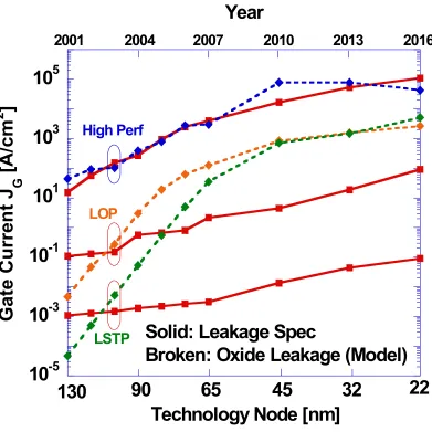
As shown in Figure 2.4, SiO2 may meet the leakage specifications for all the high
performance nodes, but oxide will not met the low power leakage requirements in 2003.
Figure 2.5 shows experimentally measured gate leakage currents for three oxynitride
films compared to the data for thermal SiO2 films of similar thicknesses [5], where it was
observed that oxynitride has less leakage than the oxide [5], especially for thinner films.
Figure 2.6 depicts the leakage currents for different oxynitride composition [6]. As shown
in the minimum of the contour, optimized oxynitride (around 60% nitride composition)
has about 100 times less leakage than oxide. As a result, optimized oxynitride may meet
the leakage spec for low operating power. High-K will be first needed for low standby
power applications around the year 2005.
2.3.2. The Tradeoff between Dielectric Constant, K, and Band Offset, φφφφn.
As shown in Figure 2.4, the 22nm low standby power technology node requires the
greatest reduction of leakage compared to a SiO2 reference. Accordingly for this specific
technology node, a detailed study was performed to quantify the trade-off between band
offset and dielectric constant of the potential gate dielectric candidates, which meet the
leakage requirements. As shown in Figure 2.1, dielectric thickness and band offset are
18
properties such as K, band offset and effective mass, which are required in the
UTQUANT simulation are not very well known. In this simulation study, the dielectric
constant and band offset were mostly based on the published results (Table 2.3 [7]). For
the effective mass a fixed value of m* of 0.5m0 (m* for SiO2) was chosen for all the
dielectrics in this study based on the good agreement between data and model for SiO2,
shown in previous section. Attempts to more precisely determine verify m* of high-K
dielectrics for use in UTQUANT will be presented in the next section.
Having fixed the effective mass, the leakage currents of materials were calculated by
UTQUANT using known two physical properties (dielectric constant and the band offset).
Statistical design of experiments (DOE) software (E-CHIP and SAS JMP 4.0) were
used to generate response surface leakage current contours. In this design of experiments
(DOE), a central composite design was used. The central composite design is the
theoretically effective way to generate a response surface, i.e., a contour plot [8]. In table
2.3, the dielectric constants and the band offsets used to generate the contour is described.
Using the contour assessed with the 22nm node, i.e., 0.056A/cm2, figure 2.7 gives the
trade-off between K and band offset, which could be used to select the proper high-K
materials for this node. For potential candidate with known K and band offset which sit
on the right side of the contour, then chances will be high for that material to meet the
leakage requirement for the 22nm low standby power node. In this projection several
high-K gate dielectric candidates are seen to satisfy the requirements.
19
An attempt to validate UTQUANT with PVD HfO2 dielectric has been made. To have
valid dielectric parameters, first, dielectric constant values were calculated from a TEM
analysis of thickness. The physical thickness of a 1.2nm EOT PVD HfO2 film from Prof.
J. Lee’s group was seen to be 5nm [9], implying a K of 17 (5nm/1.2nm x 3.9). For the
effective mass, different research group have claimed different numbers. Professor Ma’s
group showed effective mass of 0.1m0 for JVD HfO2 with their temperature dependent
leakage measurements [10], and Prof. Banerjee recently showed good data-simulation
agreement for ZrO2 with m* of 0.35m0 using a recent version of UTQUANT [11], which
is capable of simulating a double layer gate stack. Y.T. Hou, et al (Prof. D.L. Kwong
group) have reported 0.18m0 for their HfO2 [12].
To describe best value of effective mass for use in UTQUANT 2.0, an iteration has
been performed. Figure 2.8 compares simulated leakage for m* ranging from 0.3~0.5m0
with measured leakage for PVD HfO2. As shown in figure, the experimental data is
bracketed by simulations with m* = 0.3m0~0.4m0. The UTQUANT 2.0 simulated leakage
depended more strongly on voltage than experimental data. One reason for this
discrepancy may be because we actually have a multi-layer dielectric. The updated
UTQUANT showed good agreement with data using double layer simulation for ZrO2
dielectrics. Precise simulations with the newer version of UTQUANT are needed to help
improve the agreement and to better determine effective mass.
2.4. Conclusions
The projected gate leakage currents of oxide and high-K dielectrics were compared to
20
requirements for high performance nodes and optimized oxynitride appear to satisfy the
low operating power nodes. But high-K is needed for low standby power applications
around year 2005.
The material requirements for low standby power were assessed in this study using a
statistical data analysis and design of experiments techniques. As a result, leakage
contours to screen out the high-K dielectric candidates were generated. Based on this
analysis, several candidates were seen to meet the requirements for the most demanding
21
Chapter 2 References
[1] International Technology Roadmap for Semiconductors (ITRS), 2001 Edition, Dec., 2001, Semiconductor Industry Association
[2] W.-K. Shih et al., “UTQUANT 2.0 User’s Guide,” Austin, TX: Univ. Texas Press (1997)
[3] S. Mudanai, Y. Fan, Q, Quyang, A.F. Tasch, S.K. Banerjee, “ Modeling of Direct Tunneling Current Through Gate Dielectric Stacks,” IEEE Trans. Elec. Dev., Vol. 47, No. 10, p.1851 (2000)
[4] S.-H. Lo, D. A. Buchanan, Y. Taur, and W. Wang, "Quantum-Mechanical Modeling of Electron Tunneling Current from the Inversion Layer of Ultra-Thin-Oxide nMOSFET's," IEEE Elec. Dev. Lett., Vol. 18, No. 5, 209-211 (1997)
[5] T.P. Ma, “Making Silicon Nitride Film a Viable Gate Dielectric,” IEEE Trans. Elec. Dev., Vol 45, No. 1, p.680 (1998)
[6] H. Yang and G. Lucovsky, “Integration of Ultrathin (1.6~2.0 nm) RPECVD Oxynitride Gate Dielectrics into Dual Poly-Si Gate Submicron CMOSFETs,” Electron Devices Meeting, IEDM Tech. Dig., p. 245 -248 (1999)
[7] G.D. Wilk, R.M. Wallace, J.M. Anthony, “ High-K Gate Dielectrics: Current Status and Materials Properties,” Appl. Phys. Vol. 89, No. 10, p.5243 (2001)
22
[9] B.H. Lee, R. Choi, L. Kang, S. Gopalan, R. Nieh, K. Onishi, Y. Jeon, C. Kang and J.
Lee, “Characteristics of TaN Gate MOSFET with Ultrathin Hafnium Oxide (8Å ~12Å),”
IEDM Tech. Dig., p.39 (2000)
[10] W.J. Zhu, Tso-Ping Ma, T. Tamagawa, J. Kim, Y. Di, “Current Transport in Metal/Hafnium Oxide/Silicon Structure,” IEEE Elec. Dev. Lett., Vol. 23, No. 2, p.97 (1998)
[11] Y. Fan, R.E. Nieh, J.C. Lee, G. Lucovsky, G.A. Brown, L.F. Register, S.K. Banerjee, “Voltage and Temperature Dependent Gate Capacitance and Current Model: Application to ZrO2 n-channel MOS Capacitor,” IEEE Trans. Elec. Dev., Vol. 49, No. 11, p.1969 (2002)
[12] Y.T. Hou, M.F. Li, H.Y. Yu and D.-L. Kwong, “Modeling of Tunneling Currents Through HfO2 and (HfO2)x(Al2O3)1-x Gate Stacks,” IEEE Elec. Dev. Lett., Vol. 24, No. 2,
p. 96 (2003)
[13] S.K. Han, “Fabrication and Characterization of Alternative Gate Stack Devices Using Non-self Aligned Process,” Ph.D. Dissertation, Chapter 5, NCSU (2003)
[14] J. R. Hauser and K. Ahmed, “Characterization of Ultra-thin Oxides Using Electrical C-V and I–V Measurements,” Characterization and Metrology for ULSI Technology, Seiler et al., Eds. Woodbury, NY: AIP, p. 235 (1998)
[15] R. Lake et al., “Single and Multiband Modeling of Quantum Electron Transport through Layered Semiconductor Devices,” J. Appl. Phys., Vol. 81, p. 7845 (1997)
23
[17] Berkeley Device Group Available at www.device.eecs.berkeley.edu/qmcv/html [18] A.R. Hefner, C.A. Richter and E.M. Vogel, “A Comparison of Quantum-mechanical Capacitance-Voltage Simulators,” IEEE Elec. Dev. Lett., Vol. 22, No. 1, p.35 (2001)
[19] K. Yang and C. Hu, “ MOS Capacitance Measurements for High-Leakage Thin Dielectrics,” IEEE Trans. Elec. Dev., Vol. 46, No. 7, p.1500 (1999)
[20] K. Ahmed, E. Ibok, G.C.–F. Yeap, Q. Xiang, B. Ogle, J.J. Wortman, J.R. Hauser, “Impact of Tunnel Currents and Channel Resistance on the Characterization of Channel Inversion Layer Charge and Polysilicon-Gate Depletion of Sub-20Å Gate Oxide MOSFET’s,” IEEE Trans. Elec. Dev., Vol. 46, No. 8, p.1500 (1999)
[21] G.M Yeric, A.F Tasch, and S.K. Banerjee, “ A Universal MOSFEET Mobility Degradation Model for Circuit Simulation,” IEEE Trans. Computer-Aided Design, Vol. 9, p.1123 (1991)
[22] J.R. Hauser, “Extraction of Experimental Mobility Data for MOS Devices,” IEEE Trans. Elec. Dev., Vol. 43, 1981 (1996)
[23] J.T. Watt and J.D. Plummer, “ Universal Mobility-Field Curves for Electrons and Holes in MOS Inversion Layers,” Symp. On VLSI Tech. Dig., p.81 (1987)
[24] Z.J. Luo, T.P. Ma, T. Tamagawa, “Little Mobility Degradation in MOSFETs with ZrO2 High-K Gate Dielectric,” IEEE Trans. Elec. Dev., (2002)
[25] W.W. Abadeer, “Reliability Monitoring and Screening Issues With Ultrathin Gate Dielectric Devices,” IEEE Trans. Elec. Dev., Vol 1, No. 1, p.60 (2001)
24
[25] K. Onishi, C.S. Kang, R. Choi, H. Cho and J. Lee, “Reliability Characteristics, Including NBTI, of Polysilicon Gate HfO2 MOSFETs,” IEDM Tech. Dig., p.659 (2001)
[26] E.P. Gusev, D.A. Buchanan, E. Cartier, A. Ajmera, N. Bojarczuk, A. Callegari, K. Chan, M. Copel, C. D'Emic, D. DiMaria, R.J. Fleming, M.A. Gribelyuk, S. Guha, P.C. Jamison, P. Kozlowski, A. Kumar, A. Mocuta, D.A. Neumayer, H. Okorn-Schmidt, “Ultrathin High-K Gate Stacks for Advanced CMOS Devices,” IEDM Tech. Dig., p. 20 (2001)
[27] S. Zafar, A. Callegari, E. Gusev, M.V. Fischetti, “Charge Trapping in High-K Gate Dielectric Stacks,” IEDM Tech. Dig., P. 2 (2002)
[28] D. Degraeve, E. Cartier, T. Kauerauf, R. Carter, L. Pantisano, A. Kerber and G. Groeseneken, “On the Electrical Characterization of High-K Dielectrics,” MRS Bulletin March, available at www.mrs.org/publications/bulletin (2002)
[29] E. Vogel, “High-K Gate Dielectric Reliability,” MRS High-K Gate Dielectrics Workshop. New Orleans, LI, June 1-2, p.5 (2000)
[30] E. Vogel, “Modeled Tunnel Currents for High Dielectric Constant Dielectrics”, IEEE Trans. Elec. Dev., Vol. 45, No.6 (1998)
[31] Nian Yang, “Characterization and the Application of Ultra-Thin Dielectrics in Metal-Oxide-Semiconductor Devices,” Ph.D. Dissertation, NCSU (1999)
[32] Khaled Z. Ahmed “Electrical Characterization of Advanced CMOS devices”, Ph.D. Dissertation, NCSU (1998)
25
Tunneling Mechanisms Expression Comments
Direct Tunneling JTUNNELING=ATox-2exp(-2Atox)
Voltage dependence ~ V2exp(-B/V)
A,B: Constants
Tox: Oxide Thickness
Fowler-Nordheim
Tunneling
JFN=CEox2exp(-2DEox) C,D: Constants
Eox: Electric Field
Across the Oxide
26
Table 2.2 2001 ITRS requirements for EOT, Vdd and Jg.3 data sets for each column; high performance, low operating power and low standby power application (from the left) LSTP LOP HP LSTP LOP HP LST P LO P HP LST P LOP HP
EOT[nm] Simulated Oxide Leakage [A/cm2] ITRS Leakage Spec
27
Material Dielectric Constant Band gap [eV] Band offset [eV]
SiO2 3.9 8.9 3.2
Si3N4 7 5.1 2
Al2O3 9 8.7 2.8
Y2O3 15 5.6 2.3
La2O3 30 4.3 2.3
Ta2O5 26 4.5 1~1.5
TiO2 80 3.5 1.2
HfO2 25 5.7 1.5
ZrO2 25 7.8 1.4
28
Tox
band offset=3.15eV
Ec Ef
Ev Ef
METAL
n-Si (Injector) Eg=1.1eV
qΦΦΦΦB
Tox
band offset=3.15eV
Ec Ef
Ev
Ef
METAL
n-Si (Injector) Eg=1.1eV
qΦΦΦΦB
29
Fig. 2.2(a) Direct tunneling through entire stack
Gate
High-K
Interfacial Layer Ec Ev Ef
Gate
High-K
Interfacial Layer Ec Ev Ef
Fig. 2.2(b) Fowler Nordheim tunneling
Gate
High-K
Interfacial Layer Ec Ev Ef
30
Circle: Measured by Lo Solid: Model by Lo Square: UTQUANT
31
Fig. 2.4 Simulated versus specified gate leakage of SiO2 for different ITRS nodes
10
-510
-310
-110
110
310
5Gate
Cu
rre
n
t J
G
[A/cm
2
]
High Perf
LOP
LSTP
Solid: Leakage Spec
Broken: Oxide Leakage (Model)
Technology Node [nm]
130
32
22
Year
65
90
2001
45
32
33
34
Fig. 2.7 Trade off between dielectric constant and band offset for low standby power 22nm node (Dielectric’s K and band offset based on [7] except HfO2)
Y2O3
HfO2
ZrO2
35
10
-810
-710
-610
-510
-410
-310
-210
-110
0-1.5
-1
-0.5
0
J
G[A/cm
2
]
V
G
[V]
Symbols : Measured Lines : UTQUANT
0.3m
00.4m
0
0.5m
0
1.2nm PVD HfO
2
. K=17,
Φ
Φ
Φ
Φ
B=1.6eV
36
Chapter 3
Device Fabrication and Evaluation of Alternative High-K Dielectrics and Gate
Electrodes Using a Non-Self Aligned Gate Process
3.1. Introduction
In this chapter, a process to form the junctions early in the process in order to reduce
the post gate stack thermal budget is described. This process was then used to fabricate
NMOS and PMOS devices in order to evaluate and compare various high-k dielectric
materials and metal gate electrode candidates. Device characteristics were measured,
including: capacitance versus voltage, gate leakage current, drain current versus gate
voltage, and drain current versus drain voltage. An MOSFET device parameter analysis
program with corrections for quantum mechanical effects [1,2] was used to extract key
device parameters, such as effective oxide thickness, metal-to-semiconductor
workfunction, substrate doping, number of interface charges, channel mobility as a
function of electric field, and the scattering parameters (NIF and L*H product).
3.2. Device Fabrication
A novel non-self aligned process has been developed to more rapidly fabricate
devices having different high K dielectrics and gate metals. This process has only 31
steps, as compared to 66 steps for a replacement gate process. This process forms the
junctions before the gate stack and thus allows the use of dielectrics and gate electrodes
that are not able to withstand normal junction annealing temperatures. Figure 3.1 shows a
37
to the gate stack, the gate electrode overlap of the junction is very critical; thus a fair
amount of overlap was designed into the mask to allow for possible misalignment
In Table 3.1, the deposition methods of high-K dielectrics and metal gate electrodes
are described [3,4,5,6,7]. Control oxides for baseline wafers were grown in an RTP
system (N2, 880˚C 50Torr, 30sec, E. Rying and J. Hauser at NCSU). Two different
sources were used for both ZrO2 and HfO2: Jet Vapor Deposition (JVD) (W. Zhu and
T.P. Ma at Yale) and Rapid Thermal CVD (RTCVD, S.J. Lee and D.L. Kwong at UT
Austin).
For ZrO2 and HfO2 films deposited by RTCVD, NH3-based interface layers were
grown at 700 °C for 10 sec prior to deposition of the high K dielectric. The RTCVD
depositions of HfO2 and ZrO2 films were performed at 500 °C for 3 min using O2 +
C16H36HfO4 or at 500 °C for 2 min using O2 + C16H36O4Zr precursors, respectively [4,5].
After the dielectric deposition, in-situ post-deposition annealing was performed in an N2
ambient at 700 – 900 °C for 30 sec for both films. JVD of ZrO2 and HfO2 were
performed at room temperature [6,7]. For JVD HfO2, N2 and N2O plasmas were
compared to an HF last treatment for pre-deposition cleaning, and N2 was compared to
forming gas for the 600˚C post deposition annealing. Films of ZrO2 had the same
cleaning processes as HfO2 and a post dielectric deposition annealing for 20min at 550˚C
in forming gas. La2O3 was deposited by reactive evaporation in an MBE system; first, La
was evaporated from a high temperature effusion cell; then the La2O3 film was grown in
an O2 ambient of 2×10⁻⁵ Torr at 600˚C [8]. For the La2O3 splits, an additional
oxide/nitride interface was added before deposition to study interface properties. Rapid
38
For gate electrodes, low-temperature (800˚C) in-situ doped (W. Kiether and J. Hauser
at NCSU [9]) and conventional disk-doped poly gates were used as a reference for
comparing other metal gate electrodes. Commercially available TaN (UHV Sputtering,
Inc) was used. Pt was deposited using magnetron sputtering, to enhance Pt adhesion to
the dielectric, a 20 min, 500˚C N2 annealing was performed after deposition.
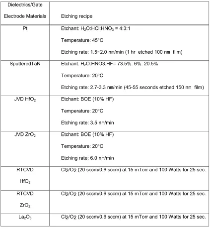
One of the major fabrication concerns was etching of gate electrodes and dielectrics.
None of these materials had any optimized wet/dry-etching recipe. For example, serious
photoresist damage was observed during aqua-regia etching of Pt, so that a short time
etch-bake-etch-bake… process was developed [10] to circumvent this problem. Table 3.2
lists the etching recipes used in our experiments.
3.3. Results and Discussions
NMOS and PMOS devices having various combinations of high-K dielectric
materials and alternative metal gate electrodes were fabricated successfully. Electrical
measurement and characterization of these devices were performed to evaluate these
materials. The width (W) and length (L) dimensions shown in the figures in this chapter
are the dimensions on the mask set. The bias in channel length (∆L) as measured delta L
by the shift and ratio method [11] was around 0.3µm.
3.3.1.Capacitance Voltage (CV) and Gate Leakage (Ig-Vg)
For HfO2 and ZrO2 dielectrics, both Pt and Al gates resulted in smooth CV
characteristics for both PMOS and NMOS (Figs. 3.2 and 3.3). But TaN gated MOS
![Table 2.3 Material properties of high-K candidates [7]](https://thumb-us.123doks.com/thumbv2/123dok_us/1351881.1168050/43.612.133.517.241.530/table-material-properties-high-k-candidates.webp)
![Fig. 2.3 The comparison of UTQUANT simulation of SiO2 leakage current with Lo model [4]](https://thumb-us.123doks.com/thumbv2/123dok_us/1351881.1168050/46.612.150.481.233.558/fig-comparison-utquant-simulation-sio-leakage-current-model.webp)