Abstract: The basic element in sequential circuit design is flip-flop and flip-flip-flops are widely used in memories. This paper outlines the design of Single-Phase Clocking flip-flop using various methods like pass transistor and the transmission gate logic. The main scope of this paper is to design a flip-flop with optimized power. The optimization of power and the reduction in transistor count is achieved by using transmission gates and pass transistor logic. 45nm CMOS based design technology chosen for the implementation technology. The performance metrics of Flip-flop designs were compared with different sequential circuits using transmission gate and pass transistor logic techniques. Pre-layout analysis results indicated that, proposed designs excelled in optimizing the average power. When compared with the other designs, the proposed flip-flop is designed using only 11-transistors and the average power consumption of the proposed flip-flop is bring downed to 108.9 nW. All the designs are simulated and verified with PYXIS tool running on 3.41 GHz processor. These flip-flop designs are best suited for low power and high performance applications.
Keywords: Transmission Gate, Flip-flop, Low Power, Single Phase Clocking (SPC)
I.INTRODUCTION
In digital sequential system designs, the most robust and common technique to build a sequential circuit involves the use of transmission gates and pass transistors. The scaling of supply voltage is critical for low power operation. Certain sequential circuits don’t function at reduced supply voltages without scaling of device thresholds. Many solutions are being explored to address the problems, the shaded inverters and transmission gates are implemented in low-threshold devices. In digital sequential system designs, flip-flops are fundamental building blocks and they are used storage elements extensively. Flip-flops employ several modules such as register files, andshift registers, and FIFO. This paper describes the comparison of existing flip-flop design technologies and are designed by using transmission gate and pass transistor based logic.
Revised Manuscript Received on December 22, 2018.
P. Sreelakshmi, P G Student, Dept. of Electronics &Communication Engineering,
K. Hari Kishore, Professor, Dept. Electronics & Communication Engineering
E. Raghuveera, Asst. Professor, Dept. Electronics & Communication Engineering
KVKVL Pawan Kumar, Asst. Professor, Dept. Electronics & Communication Engineering
Fazal Noor Basha, Asst. Professor, Dept. Electronics & Communication Engineering
The comparison of performance of average power and the transistor count is being played a key role in design of proposed flip flop. They adopt intensive pipelining techniques to improve the performance of sequential systems. If flip-flops were not optimized then IC manufacturing industry has several effects. In any digital circuits Very Large Scale Integration (VLSI) technology is used and the objective of the VLSI technology is to increase the density of transistors in single chip area. Optimization of flip-flops in terms of transistor count is very much needed for VLSI circuit designs [6].The flip-flop is highest power consuming component in clock distribution network. The power consumption of flip-flops play critical role and they impact the chip area flip-flop is the most commonly used element, an extensive segment of the most computerized circuits are use clock [1] for their synchronous operation. A conventional Single Edge-activated (SET) flip-flop [7] commonly latches information either on the rising or the trailing edge of the clock cycle. These flip-flops (SET) are generally designed as master slave flip-flops, [3] for example a sequential structure utilizing two latches, called master and slave respectively. The wide use of sequential logic and memory storage systems in modern electronics results in the implementation of low power and high speed design of basic D- Flip-flop [4]. In the new process technology flip-flop designs undergo continuous improvement and evolution of new design methodologies. The new flip-flop design for specific application needs such as high speed, low power and low voltage. However, while the execution increments because of scaling, the power thickness increments considerably every generation due to higher integration density. Moreover, the interest for power-sensitive structure has developed essentially because of the enormous development importable applications. The transmission gate flip flop most widely used flip flop. The design suffers from high capacity clock loading problem, it causes power consumption. Hence the optimized flip flop shows low power consumption the other advantage of the proposed flip flop will achieve power reduction in sequential circuits [2].The organization of the paper described as follows, the related work of various flip-flop designs with their flip designs is presented in section II, section III outlines the design of proposed flip-flop, and various flip-flop designs are described in section IV. Section V describes the simulation results and the paper is concluded in section VI.
Design and Analysis of Power Efficient
Single-Phase Clocking Master Slave Flip-flops
for Sequential Circuits
II.RELATED WORK
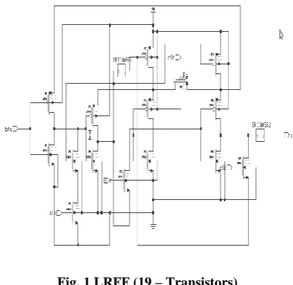
The design proposed designs in [1] abide from the power leakage problem, so to hold off this problem, the design can be optimized by considering out the common terms. For two pull down devices (nMOS), one CK-controlled transistor is shares the two discharging paths. The transistor count is decreased from 28 to 21 and just resto the transistors are directly driven by the clock signal [13].The configuration follows topologically compressed scheme, every one of these transistors aids to more power consumption. The TCFF configuration depends on the following improvement standards. They are, utilize single phase clock, number of clock driven transistors and reduction in density of transistors. In spite the basic improvement in the power, the arranging execution of the TCFF [11] configuration is extended. In particular, the design experiences a more extended setup time in view of two pMOS transistors are connected to VDD directly, and the power consumption is negatively impacted[8].To avoid from this issue the proposed structure of Fig. 1 using Logic Structure Reduction (LRFF), can be considered as an upgrade of the TCFF design in various execution aspects. This configuration is accomplished by different improvement measures. The primary measure is the logic to decrease for a shorter setup time, the second one is circuit improvement for bringing down the power, and the third one is the end of the node drifting case to maintain a strategic distance from the static power leaking issue. The advantage of this logic structure decrease is twofold. It simplifies the circuit for power saving. The circuit schematic application of the two logic structure reduction schemes is presented in Fig. 1. In this structure just 19 transistors are utilized and one single period of the clock is required, and the fan-out for the clock signal is four (one pMOS and three nMOS transistors). The proposed LRFF is completely static and can maintain a impermanent yield node drifting. In spite of the fact that the check signal fan out of the LRFF configuration is one transistor higher than that of the TCFF design. As far as circuit multifaceted nature, the LRFF utilizes minimal number of transistors.
[image:2.595.320.532.51.257.2]This can be credited to a much improved logic structure and a decreased clock signal stacking of the LRFF plan. The power advantage of the LRFF configuration limited but was still significant as the switching activity decreased. At the point when the probability of information changing decreased to 12.5%, the power savings for the two plans wound up 24% and 7%, separately [9].A logic structure decrease conspire is utilized to lessen the quantity of transistors which intends to diminish the zone for accomplishing high power and delay performance. The advantages of this logic structure reduction schemes are it simplifies the circuit for power saving and other one is low delay. Finally, the performance metrics like delay, power and number of transistors are compared with proposed flip-flop and optimized flip-flip-flop [14].
Fig. 1 LRFF (19 – Transistors)
III. WORK PROPOSED
The work proposed is the design of Flip-flop based on the transmission gates and the pass transistor logic. The key objective is to this design is to improve the performance metrics like power and the no. of transistors are used in the design and can be considered as an improvement in various design aspects. Optimization of the mentioned parameters is achieved by various measures. The former is to measure is the voltage drop problem and the latter is simplifying the design for least power consumption and it improves the feedback path. The reduction in density results in the reduction in parasitic capacitances at internal nodes of the flip-flop, this results in improved power dissipation. The feedback path in figure 2 indicates that, some of the drive current is directed in the same path, whereas rest of the drive current is directed off, the path giving rise to internal fan-out within the FF, accordingly the branching effort is given by the following expression
b= Coff-path-Con –path/ Con –path (1)
Fig. 2 Transmission Gate Flip-flop
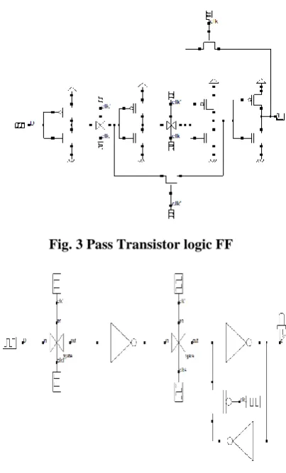
[image:3.595.69.271.240.574.2]It solves voltage drop problem Which occured in transmission gates. The internal and external nodes have less capacitance, which leads to reduction of power consumption and propagation delay. The optimized flip-flop has improved feedback path compared to Conventional FF designs.
[image:3.595.331.547.570.834.2]Fig. 3 Pass Transistor logic FF
Fig. 4 Proposed FF
Fig. 4.shows optimized flip-flop which results in less power consumption compared with previous flip-flop designs. It uses transmission gates for both master and slave flip-flops and the number of transistors were bringing down to 11, which means the area, delay and power are optimized [4].As shown in fig. 4. The NMOS output will only a voltage level of <Vddwhen it is at logic high state, power may not be optimized. The transmission gated are utilized in both master and slave design, this reduces the power dissipation. The improved feedback loop is seen in the proposed design, the majority of the traditional static structures utilize two feedback loops one each in the master and the slave. These rise in the parasitic capacitance at the internal flip-flop nodes, prompting higher dynamic power and performance degradation. This results in area overhead because of increase in transistor density. This is a low area
flip- flop and has the smallest power dissipation. Master slave flip-flops generally utilize l ow power systems. In CMOS technology D-FF is implemented with transmission gates. D type flip-flops are popular because they have fewer input signal paths and circuits using them are simpler to design. A transmission gate is formed by parallel connection of an n- channel transistor and p-channel transistor. Transmission gates have symmetric noise margins in either direction of transmission and support bidirectional signal transmission. The optimized FF exhibits better power dissipation. For low supply voltages optimized FF shows the highest delay but as the supply voltage increases its delay improves, while the delay of Proposed FF increases with increment of supply voltage as compared to other flip-flops. Optimized FF has the high delay and lowest power consumption. Optimized FF has only eleven transistors but this flip-flop has the highest delay and low power consumption, So the proposed FF is suited for low power or high performance applications. In the event that there is decrease in the quantity of timed transistors, the clock load capacitance is decreased, prompting low control utilization in the clock circulation network[6]. Hence by transistors, the power dissipation of the proposed structure is decreased.
IV. FLIP-FLOP DESIGNS
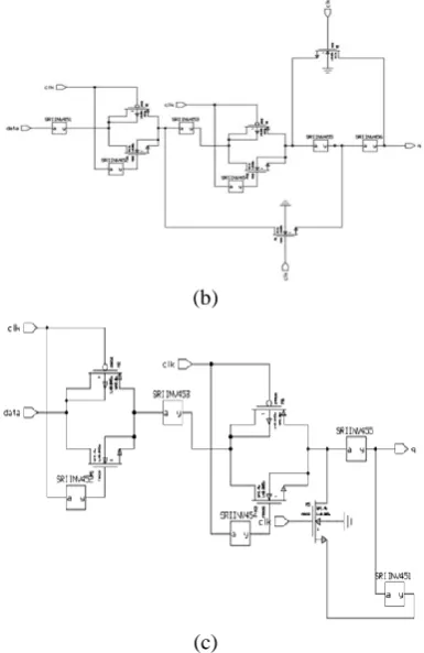
A flip-flop shown in fig 6(a) widely used in all real time applications (TGFF) [16]. To overcome the problem of power consumption two FF designs are proposed. Pass transistor based FF and optimized Fifth Fig. 6(b), pass transistor based FF uses fourteen Transistors which reduces the power dissipation. The FF has high speed of operation. It has less capacitance of nodes which reduces the power consumption as well as propagation delay. CMOS pass transistor based logic can result in speed and high-density circuits [5]. The transistor count is being reduced and to generate different logic gates, by eliminating extra transistors. Transistors are used as switches to pass logic levels between nodes of circuit, rather than switches connected on to provide voltages. The advantage is that one pass-transistor arrangement is adequate to play out the logic activity, which results in fewer transistors and smaller input loads, especially when NMOS networks are used to solve voltage drop problem.
(b)
[image:4.595.75.268.55.352.2](c)
Fig. 6 Master Slave D – Flip-flop designs (a) TGFF (b) PTFF (c) Optimized flip-flop
Fig. 6(c) shows optimized flip-flop uses eleven transistors which reduces the power consumption. One technique to decrease the transistor check is to utilize a NMOS for clock input [9]. This reduces the power dissipation. Most of the conventional static designs utilize two feedback loops one each in the master as well as the slave stage. This builds the complete parasitic capacitance at the inner flip-flop nodes, prompting higher unique power dissipation and decreased execution. This likewise results in absolute chip area overhead because of expanded transistor count [15]. In the event that there is reduction in the density of transistors, the stray capacitance is reduced, prompting effective utilization of clock network [6]. Hence by transistors, the power dissipation of the proposed structure is further decreased. This flip-flop is negative edge activated flip-flop. In the proposed FF when clock level is 'HIGH', master latch is activated and reverse of the information is put away to a between internal node. At the point when clock goes to 'LOW', slave latch moves toward becoming capacity al and produces information at the yield Q.
Rise Time and Fall Time: Rise time is predominantly varied due to stray capacitance and inductance and cause a delay in the circuit and affect the device parameters.
(2)
The above equation (2) represents parasitic capacitance, trace impedance.
Observations: Rise and fall time is independent of the data signal switching frequency. Rise or fall time can be expanded by including arrangement resistor and parallel capacitor to the each yield phase of the FF (that is stick Q). If rise or fall time can be increased at output stage. The glitches are occurred at that time. Automatically it may
consume more power. Glitches are defined as intermediate values of gates. To avoid glitches the rise and fall time must be low.
V.RESULT AND DISCUSSION
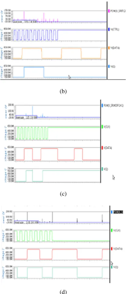
Fig. 7(a), (b), (c) & (d) represent the power consumption in nW at 0.6V supply voltage for 100 MHz clock frequency. So power dissipation rapidly reduces with reduction in the supply voltage.[15]. These figures show that rise in power with in clock frequency and decrease in supply voltage [8]. The power consumption of synchronizers is compared with master slave D flip-flop and LRFF. The optimized flip-flop consumes low power. Design and comparative analysis of Master slave D flip-flop with different techniques was done [15].Among previous flip-flops the proposed FF shows the lowest power consumption for supply voltage 0.6V and clock frequency 100 MHZ. Increase in clock frequency results in highest power consumption. Low supply voltages FF shows the highest delay but as the supply voltage increases its delay improves of Proposed FF . [14]. Table I indicates the power consumption in nW.at supply voltage 0.6V and 100MHz clock frequency. The previously proposed flip-flop shows lowest power consumption. Proposed FF has some improvement in average power consumption [13].
The proposed flip-flops discussed in section V consume least power for 0.6v supply voltage [10].low supply voltages FF shows the highest delay but as the supply voltage increases its delay improves of Proposed FF.There is always a trade-off between power dissipation and propagation delay of a circuit. A flip-flop can be reduced for either high performance or low power, but in this work, the designs are simulated to achieve low power dissipation. The simulation results indicate that the proposed FF has the least average power dissipation among all the designs for supply voltage .For fair comparison, the average power consumption when compared to the previously proposed flip-flop shows lowest power consumption. Proposed FF has some improvement in average power consumption.
[image:4.595.315.545.498.832.2](b)
(c)
[image:5.595.335.520.48.158.2](d)
Fig. 7 Simulation Results of proposed FF designs (a) LRFF (b) TGFF (c) PTFF (d) Proposed FF Fig.8 provides through analysis of the clock to Q delay under different supply voltages (from 0.6 to 1.0V). The working frequency was lowered to 100 MHz to ensure that all designs function properly in low supply voltage. In the delay analysis the proposed flip-flop shows highest delay.Fig.9 (a) and (b) provides through analysis of power under different supply voltages (0.6 to 1.0V).the proposed flip-flop shows least power consumption when compared to PTFF and TGFF.
The design and analysis of Master Slave DFlip-flopshave been done. Optimized flip-flop shows the lowest power consumption for 0.6V supply voltage and clock frequency at 100 MHz, at this frequency optimized flip-flop shows the better power consumption. Optimized flip-flop failed at 1v. As clock frequency is increased, power consumption of flip-flop increases and near 1 GHz clock frequency flip-flip-flop consumes the highest power.
Fig. 8 Performance analysis of various flip-flop designs with respect to supply voltage and clock to Q delay
(a)
(b)
Fig. 9 (a) & (b) Performance analysis of various flip-flop designs with respect to supply voltage and power
VI. CONCLUSION
[image:5.595.64.274.53.537.2] [image:5.595.326.520.192.451.2]REFERENCES
1. Jin-Fa Lin, Ming- Hwa Sheu, Yin-Tsung Hwang , Chen-Syuan Wong,
and Ming Yan Tsai, “Low-Power 19-Transistor True Single-Phase Clocking Flip-Flop Design Based on logic Structure reduction
schemes,” IEEE Transactions on very large scale integration(VLSI)
systems,vol.25, no.11, pp.3033 – 3044, July 2017.
2. H. Kawaguchi and T. Sakurai, “A reduced clock-swing flip-flop
(RCSFF) for 63% power reduction,” IEEE J. Solid-State Circuits, vol.
33, no. 5, pp. 807–811, May1998.
3. M. Matsui, “A 200 MHz 13 mm2/2-D DCT macro cell using sense
amplifying pipeline flip-flop scheme,” IEEE J. Solid-State Circuits, vol. 29, no. 12, pp. 1482–1490, Dec. 1994.
4. B. Nikolic, V. G. Oklobdzija, V. Stojanovic, W. Jia, J. K.-S. Chiu, and
M. M.-T. Leung, “Improved sense-amplifier-based flip-flop: Design and measurements,” IEEE J. Solid-State Circuits, vol. 35, no. 6,pp. 876–884, Jun. 2000.
5. V. Stojanovic and V. G. Oklobdzija, “Comparative analysis of master
slave latches and flip-flops for high-performance and low-power
systems, ”IEEE J. Solid-State Circuits, vol. 34, no. 4, pp. 536–548,Apr.
1999.
6. P. Zhao, T. Darwish, and M. Bayoumi, “High-performance and
low-power conditional discharge flip-flop,” IEEE Trans. Very Large Scale Integr. (VLSI) Syst., vol. 12, no. 5, pp. 477–484, May 2004
7. A. Makihara et al., “Hardness-by-design approach for 0.15μm fully
depleted CMOS/SOI digital logic devices with enhanced SEU/SET immunity,” IEEE Trans. Nucl. Sci., vol. 52, no. 6, pp. 2524–2530, Dec. 2005.
8. J. Furuta, J. Yamaguchi, and K. Kobayashi, “A radiation-hardened non
redundant flip-flop, stacked leveling critical charge flip-flop in a 65nm thin BOX FD-SOI process,” IEEE Trans. Nucl. Sci., vol. 63, no. 4, pp. 2080–2086, Aug. 2016
9. B.-S. Kong, S.-S. Kim, and Y.-H. Jun, “Conditional-capture flip-flop for statistic power reduction,” IEEE J. Solid-State Circuits, vol. 36, no. 8, pp. 1263–1271, Aug. 2001.
10. M.W. Phyu, K. Fu, W.L. Gohand K.S. Yeo, “Power- Efficient
Explicit-Pulsed Dual-Edge Triggered Sense-Amplifier Flip-Flops”, IEEE
Transaction onVery Large Scale Integration (VLSI) Systems, 2011, Vol. 19, No. 1, 1-9.
11. N. Kawai, “A fully static topologically-compressed 21-transistor
flip-flopwith 75% power saving,” IEEE J. Solid-State Circuits, vol. 49, no.
11,pp. 2526–2533, Nov. 2014.
12. V. G. Oklobdzija, “Clocking and clocked storage elements in a multi
gigahertz environment,” IBM J. Res. Develop., vol. 47, pp. 567–
584,1Sep. 2003.
13. C. K. Teh, T. Fujita, H. Hara, and M. Hamada, “A 77%
energy-saving22-transistor single-phase-clocking D-flip-flop with
adaptive-coupling configuration in 40 nm CMOS,” in ISSCC Dig. Tech. Papers,
Feb. 2011,pp. 338–339
14. Pradeepkumar Sharma, Bhanupriyabhargaval and syamakashe,
“Improvement of design issues in sequential logic circuit with different CMOS Design Techniques”, ISSN: 2278-0181 Vol. 3 Issue 1, January – 2014
15. Imran Ahmed khan and Mirza Tariq Beg , “Design and analysis of low
power master slave Flip-Flops,” Journal of Microelectronics,Electronic Components and Materials Vol. 43, No. 1(2013), 41 – 49.
16. M. Janaki Rani and S. Malarkann,“LLeakage Power Reduction and
Analysis of CMOS Sequential Circuits,”(VLSICS)Vol.3, No.1, February 2012.
17. Yadlapati, A., Kakarla, H.K. An Advanced AXI Protocol Verification
using Verilog HDL (2015) Wulfenia, 22 (4), pp. 307-314.
18. Bindu Bhargavi, K., Hari Kishore, K. Low Power Bist on Memory
Interface Logic (2015) International Journal of Applied Engineering Research, 10 (8), pp. 21079-21090.
19. Charan, N.S., Kishore, K.H. Recognization of delay faults in cluster based FPGA using BIST (2016) Indian Journal of Science and Technology, 9 (28).
20. Hari Kishore, K., Aswin Kumar, C.V.R.N., Vijay Srinivas, T.,
Govardhan, G.V., Pavan Kumar, C.N., Venkatesh, R.V. Design and analysis of high efficient UART on spartan-6 and virtex-7 devices (2015) International Journal of Applied Engineering Research, 10 (9), pp. 23043-23052.
21. Kante, S., Kakarla, H.K., Yadlapati, A. Design and verification of AMBA AHB-lite protocol using Verilog HDL (2016) International Journal of Engineering and Technology, 8 (2), pp. 734-741.
22. Bandlamoodi, S., Hari Kishore, K. An FPGA implementation of
phase-locked loop (PLL) with self-healing VCO (2015) International Journal of Applied Engineering Research, 10 (14), pp. 34137-34139.
23. Murali, A., Hari Kishore, K., Rama Krishna, C.P., Kumar, S., Trinadha
Rao, A. Integrating the reconfigurable devices using slow-changing key technique to achieve high performance (2017) Proceedings - 7th IEEE International Advanced Computing Conference, IACC 2017, art. no. 7976849, pp. 530-534.
24. A. Surendar, K. H. Kishore, M. Kavitha, A. Z. Ibatova, V. Samavatian
“Effects of Thermo-Mechanical Fatigue and Low Cycle Fatigue Interaction on Performance of Solder Joints” IEEE Transactions on Device and Materials Reliability, P-ISSN: 1530-4388, E-ISSN: 1558-2574, Vol No: 18, Issue No: 4, Page No: 606-612, December-2018.
25. N Bala Dastagiri K Hari Kishore “A 14-bit 10kS/s Power Efficient
65nm SAR ADC for Cardiac Implantable Medical Devices” International Journal of Engineering and Technology (UAE), ISSN No: 2227-524X, Vol No: 7, Issue No: 2.8, Page No: 34-39, March 2018.
26. N Bala Dastagiri, Kakarla Hari Kishore "Reduction of Kickback Noise
in Latched Comparators for Cardiac IMDs” Indian Journal of Science and Technology, ISSN No: 0974-6846, Vol No.9, Issue No.43, Page: 1-6, November 2016.
27. N Bala Dastagiri, K Hari Kishore "Analysis of Low Power Low
Kickback Noise in Dynamic Comparators in Pacemakers” Indian Journal of Science and Technology, ISSN No: 0974-6846, Vol No.9, Issue No.44, page: 1-4, November 2016.
28. Avinash Yadlapati, Hari Kishore Kakarla “Design and Verification of
Asynchronous FIFO with Novel Architecture Using Verilog HDL”
Jou rn a l of En gi n e eri n g a n d Ap p li ed Sc i en c es , ISSN No: 1816-949X, Vol No: 14, Issue No: 1, Page No: 159-163, January 2019.
29. Meka Bharadwaj, Hari Kishore "Enhanced Launch-Off-Capture
Testing Using BIST Designs” Journal of Engineering and Applied Sciences, ISSN No: 1816-949X, Vol No.12, Issue No.3, page: 636-643, April 2017.
30. Dr. Seetaiah Kilaru, Hari Kishore K, Sravani T, Anvesh Chowdary L,
Balaji T “Review and Analysis of Promising Technologies with Respect to fifth Generation Networks”, 2014 First International Conference on Networks and Soft Computing,ISSN:978-1-4799-3486-7/14,pp.248-251,August 2014.
31. P Bala Gopal, K Hari Kishore, R.R Kalyan Venkatesh, P Harinath
Mandalapu “An FPGA Implementation of On Chip UART Testing with BIST Techniques”, International Journal of Applied Engineering Research, ISSN 0973-4562, Volume 10, Number 14 , pp. 34047-34051, August 2015.
32. Avinash Yadlapati, Hari Kishore Kakarla “Design and Verification of
Asynchronous FIFO with Novel Architecture Using Verilog HDL”