Abstract: As the technology is improving, channel length of MOSFET is scaling down. In this environment stability of SRAM becomes the major concern for future technology. Static noise margin (SNM) plays a vital role in stability of SRAM. This paper gives an introduction to the reconfigurable memory and 6T SRAM cell. It includes the implementation, characterization and analysis of reconfigurable memory cell and its comparison with the conventional 6T SRAM cell for various parameters like read margin, write margin, data retention voltage, temperature and power supply fluctuations and depending upon these analysis we find SNM for 6T and 8T SRAM cell. The tool used for simulation purpose is IC Station by Mentor Graphics using 350nm technology at supply voltage of 2.5volts.
Index Terms: SNM, 6T SRAM, DRV, CR, 8T SRAM
I. INTRODUCTION
Now-a-days technology scaling is a continuous trend in VLSI integrated circuits which has given rise to a new application of 6T SRAM cell, known as the Reconfigurable Memory Cell. The term reconfigurable depicts the use of the memory cell in various configurations as required by the application for which it is used. Reconfigurability when added to the memory cell design makes the structure apt for a wide range of applications. This work contains implementation and characterization of 1-bit Reconfigurable memory cell. The Reconfigurable memory architecture consists of three sections: the memory, the interconnect and the interface logic. The memory section of a reconfigurable architecture contains array of memory blocks which are known as mats. Each mat can be converted to a cache, a FIFO, or scratchpad memory. The Reconfigurable memory cell is basically a 6T SRAM cell with dual port and two additional storage devices to efficiently support normal Read Modify Write operation as well as one additional operation known as Gang operation. The advantage of using Gang operation is that all cells in a column can be set or cleared in a single cycle. Thus, resulting in fast SRAM. The stability analysis of Reconfigurable memory cell has been done for various parameters such as cell ratio, pull up ratio, read margin, write margin, data retention voltage and threshold voltage which shows that this cell has improved static noise margin than the conventional 6T SRAM cell. But the Reconfigurable memory cell dissipates more
Revised Manuscript Received on June 15, 2019.
Tejinder Kaur, Electronics and Communication Engineering, CEC Landran, Mohali, Punjab, India.
Rachna Manchanda, Electronics and Communication Engineering, CEC Landran, Mohali, Punjab, India.
Chanpreet Kaur, Electronics and Communication Engineering, CEC Landran, Mohali, Punjab, India.
power than 6T SRAM cell. So, there is a trade-off between cell stability and power consumption.
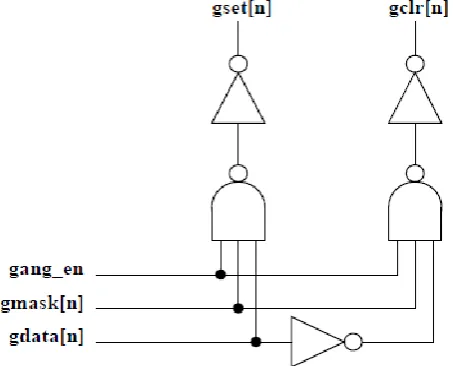
II. RECONFIGURABLE MEMORY CELL A Reconfigurable memory cell is shown in Figure 1. In this, the meta-data is tightly integrated with the main data SRAM array to share as many resources (e.g., decoder, replica control path) as possible for low overhead and high-performance. Thus, the additional storage cells namely, M0 and M1are used for the implementation of metadata in the main SRAM array as shown in Figure1. In the implemented dual port reconfigurable memory cell, generalized status bits called meta-data bits are used for each data word. The bits which hold data about the data are known as “meta-data” bits. The meta-data bits have the feature that they can be read and written along with the main data on all accesses. Additionally, there are special operations, called a gang operation that only operates on the meta-data. With the help of Gang operations all bits of the meta-data can be operated on a per-column basis in a single cycle. A gang operation can be one of the three namely, set, clear, or no operation (NOP) on any combinations of meta-data columns. The ‘gset’ and ‘gclr’ lines are shared by all the cells in a column. With the insertion of ‘gset’ all cells in a column are set to logic1 while, inserting ‘gclr’ all the cells in a column are cleared to ‘0’. The gang I/O logic for ‘gang-set’and ‘gang clear’signals is shown in Figure 2. All normal operations use port 0 i.e. WL0, b0, b0 b. Another port i.e. Port1 is a specially designed port used by read-modify-write operations.
Fig.1:-Reconfigurable Memory Cell
Parameters for Stability of Reconfigurable
Memory and 6T SRAM Cell
A.Read Operation
Both Read operation and Write operation can be performed with port0 and port1. In this paper port0 is used for read operation. Read operation is performed using word-line WL0 and MOSFETs M5, MS2 and MS3.Assuming both bit-lines to be pre-charged to logic‘1’. When Word-line WL0 is asserted, current flows in and out of the read circuit and. One of the Bit-line starts discharging to a few volts and there is a voltage rise on the associated output node i.e. at node ‘a’. The cell data is read by sensing the Bit-Line voltage fluctuation using differential current mode sense amplifier. The voltage rise at the output node ‘a’ must be low enough not to cause a substantial current through the MS4-MS3 inverter, which in worst case could flip the cell outputs. It is necessary to keep the resistance of transistor M5 larger than that of MS2 to prevent the flipping of output states.
B.Write Operation
Write operation is performed on port0 of the Reconfigurable memory cell. Write operation is performed using Word-line WL0 and MOSFETs M6, MS3 and MS4 as shown in Figure 1. Initially both the Bit-lines are pre-charged to ‘1’ and on the insertion of write enable signal one of the bit-line gets discharged. Write driver circuit is used to discharge one of the Bit-lines. Now, when the Word-line WL0 gets “ON” the outputs at node ‘a’ and ‘a_b’ is flipped from ‘1’ and ‘0’ to’ 0’ and ‘1’ respectively. The order in which the Word- line is enabled and the write drivers are activated is not crucial for the correct write operation.
C.Gang Operation
The I/O logic for gang-set and gang-clear is shown in Figure 2. Gang enable i.e. gang_en is simply an enable signal. For ‘gset’ operation all the three input signals i.e. gang_en, gmask[n] and gdata are to be made high and all the cells in a column are set to ‘1’. For ‘gclr’ operation gdata[n] is set to ‘0’ value whereas gang_en and gmask[n] are set to be at logic ‘1’ and all the cells in a column are cleared to ‘0’.When all the three signals are asserted, all the cells in a column are either set to logic ‘1’ or logic ‘0’ depending upon the signal asserted on gdata[n] input.
Fig.2: I/O logic for gset and gclr signals
III. PARAMETERS ANALYSED
In this section, different types of parameters such as Static Noise Margin (SNM), Data Retention Voltage (DRV), Read Margin (RM), and Write Margin (WM) for Reconfigurable memory cell have been analyzed. Also the calculations of both Cell Ratio (CR) and Pull-up Ratio (PR) have been done and corresponding Static Noise Margin is analyzed.
A.Static Noise Margin (SNM)
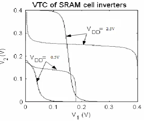
[image:2.595.305.539.384.551.2]In this section, Butterfly method for measuring static noise margin is introduced. It is the maximum amount of noise voltage that can be tolerated in a Reconfigurable memory cell while still maintaining the correct operation .Static noise margin of SRAM cell depends on the cell ratio (CR), supply voltage and pull up ratio. High value of SNM is required for the high stability of SRAM cell. Both read margin and write margin are also affected by the static noise margin of SRAM cell. SNM is also affected by the threshold voltages of NMOS and PMOS transistors. To obtain the butterfly curve, Adobe Photoshop CS7 is used. The two output curves are rotated according to X-Y coordinates which results in butterfly structure. The butterfly structure shown in Figure 3 is finally obtained. The static noise margin is a side of Maximum Square drawn between the inverter characteristics.
Fig 3: Calculation of SNM after rotation B.Cell Ratio (CR)
In this section, static noise margin is calculated by varying the cell ratio of transistors. Cell ratio is the ratio of sizes of driver transistor to the access transistor. As the cell ratio increases by increasing the size of driver transistor, Static noise margin of memory cell also increases which results in increase of current in a memory cell.
Cell Ratio (CR) = (WS2/LS2) / (W5/L5)
C.Pull up Ratio (PR)
In this section, static noise margin is calculated by varying the Pull up ratio of transistors. Pull up ratio is the ratio of sizes of load transistor to the access transistor. As the Pull up ratio increases by increasing the
[image:2.595.53.280.574.757.2]which results in increase of current in a memory cell.
Pull up Ratio (PR) = (WS3/LS3) / (W6/L6)
D. Data Retention voltage(DRV)
[image:3.595.305.542.113.250.2]In this section, Static noise margin is calculated by varying the supply voltage of a memory cell. Data retention voltage is the Minimum power supply voltage required to retain data in a high node in the standby mode of SRAM cell is known as the data retention voltage of the cell. For calculation of DRV, the power supply voltage is reduced continuously until the state of SRAM cell is not flipped or until contents of the SRAM cell remain constant and the corresponding SNM can be calculated. With the decrease in the supply voltage i.e. VDD down to DRV, the Voltage Transfer Curves (VTC) of the cross coupled inverters degrade to such a level that Static Noise Margin (SNM) of the SRAM cell reduces to zero as shown in Figure 4
Fig 4: VTC during calculation of DRV E.Read margin (RM)
[image:3.595.47.286.281.481.2]In this section, Read margin (RM) is calculated based on transistor current model. The read margin defines the read stability of the SRAM cell based on the VTC obtained. The read margin of the SRAM cell is directly proportional to the cell ratio of the cell. The value of read margin increases with the increase in value of the cell ratio. Butterfly method is used for the read margin analysis as shown in Figure 5.
Fig. 5: Calculation of Read Margin F. Write Margin (WM)
Write margin of an SRAM cell is the minimum bit line voltage required to flip the state of the cell. The value of write margin
depends on the cell design, SRAM array size and process variation. Existing bit-line (BL) sweep method is used for the calculation of Write margin as shown in Figure 6.the value of Write margin increases with increase in the Pull up ratio (PR).
Fig. 6:-Calculation of Write Margin IV. COMPARATIVE ANALYSIS
The simulation results of Reconfigurable memory cell are analyzed and compared with the conventional 6T SRAM cell for Cell ratio, Pull up Ratio, Data retention voltage, Read Margin, Write Margin, threshold variations and temperature variations and corresponding SNM is calculated in 350 nm technology with supply voltage of 2.5V.
A.Cell Ratio Vs SNM
Table 1 presents the static noise margin of Reconfigurable memory cell calculated by varying the cell ratio and comparison with 6T is done. Results show that SNM i.e. stability of Reconfigurable memory cell is---- higher than the 6T SRAM cell as it is a dual port cell thus increases the stability of memory cell.
Cell Ratio (CR) = (WS2/LS2) / (W5/L5) = 1.2
B.Pull up Ratio Vs SNM
Table 2 presents the static noise margin of Reconfigurable memory cell calculated by varying the Pull up ratio and comparison with 6T is done. Results show that SNM i.e. stability of Reconfigurable memory cell is higher than the 6T SRAM cell as it is a dual port cell thus increases the stability of memory cell.
Pull up Ratio (PR) = (WS3/LS3) / (W6/L6) = 2.1
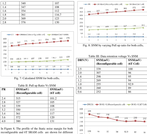
[image:3.595.46.279.612.740.2]In Figure 7, The profile of the Static noise margin for both reconfigurable and 6T SRAM cells are shown for different cell ratios.Here the Reconfigurable cell has better SNM than 6T cell.
Table I: Cell ratio Vs SNM
CR SNM(mV)
(Reconfigurable cell)
SNM(mV) (6T SRAM)
0.6 309 100
0.8 317 102.5
[image:3.595.307.552.647.831.2]1.2 340 107
1.4 347 108
1.6 354 112
1.8 361 116.7
2.0 369 123
2.8 376 130
Fig. 7: Calculated SNM for both cells.
Table II: Pull up Ratio Vs SNM
PR SNM(mV)
(Reconfigurable cell)
SNM(mV) (6T cell)
2.4 315 101.2
2.8 327 105
3.0 339 108
3.2 350 113
3.4 361 117
3.6 372 120
4.0 380 131
In Figure 8, The profile of the Static noise margin for both reconfigurable and 6T SRAM cells are shown for different Pull up ratios. Here the Reconfigurable cell has better SNM than 6T cell.
C.Data Retention Voltage Vs SNM
Table 3, presents the Static noise margin of Reconfigurable memory cell calculated by reducing the power supply voltage until the states of cell are not flipped and comparison with 6T is also done. Results show that static noise margin decreases with decrease in supply voltage but the SNM of Reconfigurable memory cell is better than the 6T cell. The value of DRV for 350nm technology is 0.5V.
[image:4.595.44.541.46.499.2]In Figure 9, The profile of the DRV for both the cells are shown for different power supply voltages at 350nm technology .Here the Reconfigurable memory cell has better SNM than 6T cell.
[image:4.595.306.555.234.552.2]Fig. 8: SNM by varying Pull up ratio for both cells.
Table III: Data retention voltage Vs SNM
DRV(V) SNM(mV)
(Reconfigurable cell)
SNM(mV) (6T Cell)
2.5 339 100
2.0 307 96
1.6 298 95
1.2 269 94
1.0 255 92.9
0.8 260 89
0.6 252 86
Fig. 9: Calculated SNM by varying supply voltage for both cells
D.Read Margin Vs SNM
Table IV: Read Margin Vs SNM
CR Read Margin
(Reconfigurable cell)
Read Margin (6T SRAM)
0.8 0.539 0.194
1.0 0.550 0.196
1.2 0.563 0.200
1.4 0.572 0.209
1.6 0.579 0.211
1.8 0.585 0.215
2.0 0.591 0.221
[image:5.595.46.282.283.431.2]In Figure 10, The profile of the Read Margin for both the cells are shown for different values of cell ratio at 350nm technology. Here the Reconfigurable memory cell has better Read Margin than 6T cell.
Fig. 10: Calculation of RM by varying CR E.Write Margin Vs SNM
Table 5, presents the Write Margin of Reconfigurable memory cell calculated by varying the Pull up ratio and comparison with 6T is also shown. Write margin of Reconfigurable cell is directly proportional to Pull up ratio i.e. write margin increases when Pull up ratio increases.
[image:5.595.293.550.340.586.2]In Figure 11, The profile of the Write Margin for both the cells are shown for different values of Pull up ratio at 350nm technology. Here the Reconfigurable memory cell has better Write Margin than 6T cell.
Table V: Write Margin Vs SNM
PR Write margin
(reconfigurable cell)
Write margin (6T SRAM)
3.0 0.752 0.246
3.2 0.768 0.249
3.4 0.776 0.253
3.6 0.786 0.256
4.0 0.792 0.261
4.2 0.803 0.269
Fig. 11: Calculation of WM by varying PR F. Threshold voltage Vs SNM
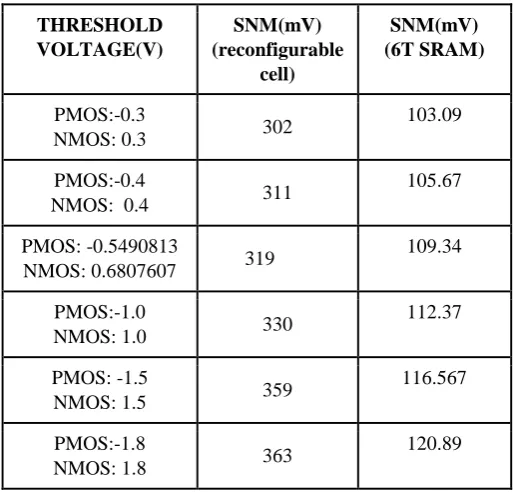
Table 6, presents the Static Noise Margin of Reconfigurable memory cell calculated by varying the threshold voltages of both NMOS and PMOS transistor and comparison with 6T is also shown. Static noise margin decreases with decrease in threshold voltages of both NMOS and PMOS transistors
Table VI: Threshold Voltage Vs SNM
In Figure 12, The profile of the SNM for both the cells are shown for different values of threshold voltage for both NMOS and PMOS at 350nm technology. Here the Reconfigurable memory cell has better noise tolerance at low values of threshold voltage than 6T SRAM cell.
THRESHOLD VOLTAGE(V)
SNM(mV) (reconfigurable
cell)
SNM(mV) (6T SRAM)
PMOS:-0.3
NMOS: 0.3 302
103.09
PMOS:-0.4
NMOS: 0.4 311
105.67
PMOS: -0.5490813
NMOS: 0.6807607 319
109.34
PMOS:-1.0
NMOS: 1.0 330
112.37
PMOS: -1.5
NMOS: 1.5 359
116.567
PMOS:-1.8
NMOS: 1.8 363
892
Published By:
Blue Eyes Intelligence Engineering & Sciences Publication
Retrieval Number: I11430789S19/19©BEIESP DOI: 10.35940/ijitee.I1143.0789S19
Photo
-2 Fig. 12: Calculation of SNM by varying Threshold voltage
G.Delay Analysis
In this section, Write time, Gang set time and Gang clear time is calculated for the one bit Reconfigurable memory cell. The calculated ‘Write time’ is 0.96634ns. The ‘Gang set time’ is 0.983601ns and ‘Gang clear time’ is 1.31148 ns.
H.Noise Analysis
In this section, both RMS noise and Transient noise has been calculated for Reconfigurable memory cell. The calculated value of RMS Noise at two output nodes ‘Q’ and ‘Qbar’ is 16.421 V and 17.331 V respectively while the transient noise at output nodes ‘Q’ and ‘Qbar’ is 1.2244 V and 1.2255 V respectively.
V. CONCLUSION
In this paper, stability analysis for various parameters such as read margin, write margin and data retention voltage for reconfigurable memory cell has been done. Also, the results are compared with conventional 6T SRAM cell. From the above analysis it can be concluded that Static Noise Margin (SNM) of Reconfigurable Memory cell is better than the conventional 6T SRAM cell.
REFERENCES
[1]. Ken Mai, “Design and analysis of Reconfigurable Memories”, Dissertation, Stanford University, 2005.
[2]. Andrei Pavlov & Manoj Sachdev, “CMOS SRAM Circuit Design and Parametric Test in Nano-Scaled Technologies”, Intel Corporation, University of Waterloo, 2008 Springer Science and Business Media B.V., pp: 1-202.
[3]. K. Mai et al., “Smart Memories: A Modular Reconfigurable Architecture,” Proceedings, International Symposium on Computer Architecture, pp. 161-71, June 2000.
[4]. Ken Mai, Ron Ho, Elad Alon, Dean Liu, Younggon Kim, Dinesh Patil, and Mark A. Horowitz, “Architecture and Circuit Techniques for a 1.1-GHz 16-kb Reconfigurable Memory in 0.18 micron CMOS”, IEEE Journal of Solid-State Circuits, vol. 40, 2005, pp:261-275.
[5]. Qiaoyan Yu and Paul Ampadu “Cell Ratio Bounds for Reliable SRAM Operation”, IEEE, 2006, pp: 1192-1195.
[6]. Kumar, A.; Qin, H.; Ishwar, P.; Rabaey, J.; Ramchandran, K.; “Fundamental Bounds on Power Reduction during Data-Retention in Standby SRAM” ; IEEE International Symposium, vol. 27(30), 2007, pp. 1867 – 1870.
[7]. Debasis Mukherjee, Hemanta Kr. Mondal and B.V.R. Reddy, “Static Noise Margin Analysis of SRAM Cell for High Speed Application”, IJCSI International Journal of Computer Science Issues, vol. 7, 2010.
[8]. B. Amrutur and M. Horowitz, “Speed and Power Scaling of SRAM’s,” IEEE Journal of Solid-State Circuits, 2000.
[9]. E. Seevink and F. List, “Static Noise Margin Analysis of MOS SRAM Cells”, Solid-State Circuits, IEEE Journal of, vol. 5, 1987, pp. 748-754.
[10] L. Chang, D. Fried and J. Hergenrother, “Stable SRAM cell design for the 32 nm node and beyond”, VLSI Technology, 2005. Digest of Technical Papers. 2005 Symposium on, 2005, pp. 128-129.
AUTHORSPROFILE
Tejinder Kaur is working as Assistant Professor at CEC Landran. She Completed M-tech from PITK, PTU Main Campus Jalandhar. She has published more than 5 publications reputed Journals and conferences. Her interest areas include WSN and VLSI.
Rachna Manchanda is working as Assistant Professor at CGC Landran. She has published more than 30 publications in reputed Journals and conferences. Her Interest include Digital System design and Front end VLSI.
[image:6.595.50.289.50.199.2]