A Fully Differential Gain Boosted Folded
Cascode OTA with 100dB Gain
Mohammed Arifuddin Sohel 1, Maliha Naaz 2, M.A. Raheem 2, Md. Afroze3
Associate Professor, Dept. of ECE, Muffakham Jah College of Engineering and Technology, Hyderabad, India1 Assistant professor, Dept. of ECE, Muffakham Jah College of Engineering and Technology, Hyderabad, India2
Verification Engineer, Wipro Technologies, Bangalore. India3
ABSTRACT: A design methodology with practical considerations for the design of Gain boosted fully differential Folded Cascode OTA along with Common Mode Feedback (CMFB) circuit is presented. An optimum OTA topology is done in order to optimize MOS Transistor sizing. Simulation results are performed using CADENCE software in 0.18µm process technology. Simulations using 0.18µm process show a DC Gain of 100dB and a Phase Margin of 65º at Unity Gain Bandwidth of 650MHz.
KEYWORDS: CMFB, OTA, Folded cascode, Gain Boosting.
I.INTRODUCTION
Operational amplifiers (usually referred to as op-amps) are key elements in analog processing systems. Ideally they perform the function of a voltage controlled current source, with an infinite voltage gain.
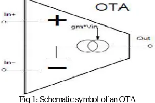
The operational trans-conductance amplifier (OTA) is basically an op amp without an output buffer. An OTA without buffer can only drive capacitive loads. An OTA can be defined as an amplifier where all nodes are low impedance except the input and output nodes. In an OTA differential input voltage produces an output current. Thus, it is a voltage controlled current source (VCCS). There is usually an additional input for a current to control the amplifier's trans-conductance. The schematic symbol of an Ideal OTA is represented in figure 1.
Fig 1: Schematic symbol of an OTA
Fully differential (FD) operational amplifiers are core elements for the design of analog high performance systems. These elements are used in a wide variety of applications, such as audio amplifiers, analog filters, data converters (D/A and A/D), modulators, instrumentation, etc. The fully differential operation provides many advantages over its single ended counterpart, such as, rejection to input common mode signals (i.e. noise), much lower power supply sensitivity (PSS), higher output dynamic range, and second order harmonics reduction. However high gain FD circuits require common mode feedback (CMFB).
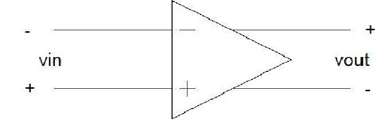
The differential op amp has two input signals, Vi1 and Vi2, and two output signals, VO1 and VO2.However, the input
and output signals of interest in this system is the difference between the two input terminals and the two output terminals, respectively [1]. The difference between these signals is called the differential mode input and differential mode output, or ViDM and V0DM. If this is a balanced system with balanced inputs, the input and output signals can be
referenced to a common mode, or average voltage, ViCM and VoCM, respectively as shown in figure 3. If the common
Fig 2: Differential input signal and differential output signal
Fig 3: Symbol of fully differential op amp
This paper is organized as follows. Section II consists of the Design of CMFB circuit, Section III describes about the Gain Boosting Technique using Auxiliary Amplifier Circuit which is used for biasing, Section IV describes an approach for designing this OTA, clarifies specific design issues and results. Section V presents the result summary and Section VI provides the concluding remarks.
II. CMFB CIRCUIT
A. Common Mode Feedback
A CMFB loop is used to stabilize the output common mode (CM) voltage in differential circuits. The output CM level is very sensitive to device properties and mismatches, and cannot be precisely defined in the presence of differential feedback. Thus a CMFB loop must sense the CM output level, compare it to the reference CM value and accordingly adjust one of the bias voltages of the amplifier to correct the output CM voltage and force it towards the reference value [2].
There are two different types of CMFB networks: continuous (CMFB) and switched-capacitor (SCMFB). C-CMFB circuits are more suitable for continuous-time applications where the output is valid at all times. SC-C-CMFBs are mostly used in discrete type applications where the output is valid in one phase of the clock and the effect of feed through can be tolerated. Here C-CMFB is designed and analyzed accordingly.
B. Circuit Design
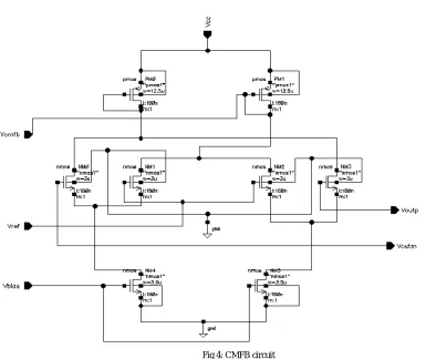
CMFB is necessary in a fully differential OTA to keep the outputs from drifting high or low out of the range where the amplifier provides plenty of gain. Continuous time CMFB has been chosen for our OTA design. CMFB circuit shown in Figure 4 is based on a standard design [3].
It uses two differential pairs (M1, M2 and M4, M5) to sense the difference between the average output voltage and a common mode voltage VCM or Vref which is supplied externally.
Vcmfb is used to bias a transistor that adds to the bias current and keeps the common mode from drifting up as shown
Fig 4: CMFB circuit
The current in the CMFB circuit does not need to be large as long as the currents through the top and bottom of the OTA are fairly well balanced. The current through CMFB is small so that the power dissipation also small [4].
The calculated (W/L) values of CMFB circuit are given in the following table:
TABLE 1
TRANSISTOR SIZES OF THE CMFB CIRCUIT
Transistor W (µm) L (nm) Transistor W (µm) L (nm)
M1 3 180 M5 3.5 180
M2 3 180 M6 3.5 180
M3 3 180 M7 12.5 180
M4 3 180 M8 12.5 180
III.GAIN BOOSTING TECHNIQUE
The gain-boost technique is based on increasing the cascoding effect of T2 by adding an additional gain stage as shown in the figure 6.
Fig 6: Cascode gain stage with Gain Enhancement
This stage reduces the feedback from the output to the drain of the input transistor. Thus, the output impedance of the circuit is increased by the gain of the additional gain stage, Aadd. In this way, the dc gain can be increased several orders of magnitude as seen in equation 3.1
A0, total=gm1r01(gm2r02(Aadd+1)+1)
(1) A. Auxiliary Amplifier
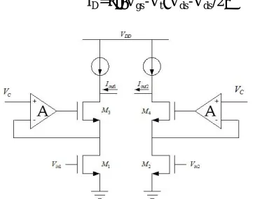
The idea of transconductors using constant drain-source voltages is to keep the input devices in triode region such that the output current is linearized. The schematic of this method is shown in Figure 7. Considering that transistors M1,
M2operate at triode region, M3, M4are biased at saturation region, channel length modulation, body effect, and other
second-order effects are ignored, the drain current of M1and M2is given by 3.2.
ID=β Vgs-Vt Vds-Vds 2
/2 (2) where β =µnCox(W/L)
Fig 7: Transconductor using constant Drain-Source Voltage
The Transfer Characteristics of this transconductor is given by
Iout=Iout1-Iout2=βVc(Vin1-Vin2)
B. Design of Auxilary Amplifier:
The amplifier consists of a PMOS current mirror, a Differential pair for inputs and an NMOS current mirror at the bottom.
Fig 8: Auxiliary Amplifier Circuit TABLE 2
TRANSISTOR SIZES OF AUXILIARY AMPLIFIER CIRCUIT
Transistor W (µm) L (µm) Transistor W (µm) L (µm)
M1 15 1 M4 10 1
M2 15 1 M5 4.5 1
M3 10 1 M6 4.5 1
IV.GAIN BOOSTED FOLDED CASCODE OTA
To show folded cascade OTA performances, this paper is interested in OTA design carrying. This design follows synthesis procedure based on the Gm/ID methodology [5].
A. Sizing Algorithm
MOS transistors are either in strong inversion or in weak inversion. The design methodology based Gm/ID
characteristic, proposed by allows a unified synthesis methodology in all regions of operation the MOS transistor. We consider the relationship between the ratio of the transconductance Gm over the DC drain current ID, and the normalized
drain current ID/ (W/L) as a fundamental design relation [5]. Gm/ID is based on its relevance for the following reasons:
It is strongly related to the performance of analog circuits. It gives an indication of the device operation Region.
It provides a simple way to determine the transistor dimensions.
The (W/L)’s of the OTA circuit is calculated using the following equations (4-7) Assuming Cl=0.3pf
Gm = 2πω×Cl (4)
Iss= Slew Rate × Cl (5)
Iss = (w/l)(Vgs−Vt) (6)
= 2 ×
B. OTA Design
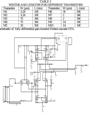
After applying the design strategy, we obtained the parameters, computed and summarized in Table 3
TABLE 3
WIDTHS AND LENGTHS FOR DIFFERENT TRANSISTORS Transistor W (µm) L (nm) Transistor W (µm) L (nm)
M1 3.24 180 M6 30 500
M2 3.24 180 M7 2 360
M3 70 360 M8 2 360
M4 70 360 M9 14 180
M5 30 500 M10 14 180
Figure 9 shows the schematic of fully differential gain boosted Folded cascade OTA.
Fig 9: Fully Differential Gain Boosted FC OTA
C. Results
The designed Gain Boosted Folded Cascode OTA was biased at 1.8V power supply voltage using CMOS technology of
0.18μm.
Fig 10: Input & Output Waveforms of Gain Boosted FC OTA
2. AC Analysis: A sine wave of 10 KHz frequency, 100mV p-p is given as input to OTA. The AC response is as shown in the figure 2.18. The DC gain of the Gain Boosted Fully Differential FC OTA is 100dB and Unity Gain Bandwidth is 650MHz, phase margin of 180-115=65º.
Fig 10: AC Response of Gain Boosted Folded Cascode OTA
V
.
RESULT SUMMARYTABLE 4
Table 4 shows the summary of the results obtained from the design of Gain boosted Folded cascode OTA.
Specifications Results
Technology Size 180nm
DC Gain 100 dB
UGB 650 MHz
Supply Voltage ±1.8V Slew Rate 100V/µs Phase Margin 65º
Load 0.5pf
VI. CONCLUSION
Future work would involve the exploitation of these results on folded cascode OTA for low power consumption and applications to use it Sigma Delta analog-to-digital converters.
REFERENCES
[1] S. Kishk, M. Abo-Elsoud and A. Osman “Design of Low Voltage 1st Order 3-Bit Quantizer SR ΔΣ Modulator Using SR Op-Amp” ASAT-13-CM-11.
[2] B. Razavi, Design of Analog Cmos Integrated Circuits. New York, NY:McGraw-Hill, 2001.
[3] Raghuwar Sharan Gautam, P.K.Jain, D.S.Ajnar “Design of Low Voltage Folded Cascode Operational Transconductance Amplifier with Optimum Range of Gain and GBW in 0.18µm Technology”, International Journal of Engineering Research and Applications (IJERA) Vol. 2, Issue 1,Jan-Feb 2012, pp.566-570.
[4] “A Self-Biased High Performance Folded Cascode CMOS Op-Amp”, IEEE 2006 by S Pradip Mandal and V.Viisvanathan.
[5] F. Silveira, D. Flandre et P.G.A. Jespers, "A gm/ID based methodology for the design of CMOS analog circuits and its application to the synthesis of a SOI micropower OTA", IEEE J. of Solid State Circuits, vol. 31, n. 9, sept. 1996.
[6] S. Mallya and J. Nevin, “Design procedures for a fully differential folded-cascode cmos operational amplifier,” IEEE J. of Solid-State Circuits, vol.24, no.6, pp.1737–1740, Dec 1989.