Design and Realization of an Arithmetic Unit
using Fredkin Reversible Gate
Parul V. Sindhwad1
Assistant Professor, Dept. of Electronics & Telecommunication, K.J. Somaiya College of Engineering, Mumbai,
Maharashtra, India1
ABSTRACT: When we use irreversible gate, there is loss of information which result in energy loss. Hence reversible
logic gates which provide low power consumption has become the most promising research areas in recent times. Reversible logic designs have several applications which includes nanotechnology, digital signal processing, quantum computing, optical computing, low power CMOS and many more. Feynman Gate, Fredkin Gate, and Peres Gate are few of the important reversible gates used for reversible logic design. In this paper an Arithmetic Unit using Fredkin Gate is proposed.
KEYWORDS: Reversible Gate, Arithmetic Unit, Fredlkin Reversible Gate, Peres Gate, BKG Gate, Reversible Full
Adder
I.INTRODUCTION
Energy dissipation is one of the huge concern in recent day technology. In the year 1960 R. Landauer demonstrated energy dissipation due to high technology circuits and system designed with irreversible hardware. According to him the loss of one bit of information lost, will dissipate kT*ln (2) joules of energy where, k is the Boltzmann’s constant, T is the absolute temperature [1]. Bennett proposed a solution to the problem of heat dissipation. Bennetee [2] showed in order to avoid kT*ln (2) joules of energy dissipation in a circuit it must be built from reversible circuits. Reversible circuit do not lose information. A circuit will be reversible if input vector can be specifically retrieved from output vectors and here is one to one correspondence between input and output [3].
The main challenges to design a reversible circuit are [4] [11]
Number of Gates: Minimum possible number of gates should be used to design the circuit
Garbage Output: The number of unwanted output should be minimum
Hardware Complexity: It refers to the total number of logic operation in a circuit.
Flexibility: It refers to the universality of a reversible logic gate in realizing more functions.
Quantum Cost:Cost of the circuit in terms of the number of primitive gates used to design it
ALU works as a data Processing unit which is an important part in Central Process Unit (CPU). ALU works continuously during the life time of any computational device, hence reversible logic can be implemented in designing ALU to reduce the power dissipation and propagation delay in the circuits [5]. In this Paper we have proposed two designs 1. Arithmetic Unit with Fredkin Gate and Peres Gate 2. Arithmetic Unit withFredkin Gate and BKG Gate
II.RELATE WORK
A. Reversible Logic Function
gate which is also known as CNOT gate. The V and V+ Quantum gates have the property given in the Equations 1, 2 and 3.
V * V = NOT ……… (1) V * V+ = V+ * V = I ………. (2) V+ * V+ = NOT ………. (3)
The Quantum Cost of a Reversible gate is calculated by counting the number of V, V+ and CNOT gates. [6]
B. Reversible Logic Gates
NOT Gate
The Reversible 1*1 gate is NOT Gate with zero Quantum Cost is as shown in the Fig 1. [7]
Fig.1 NOT Gate
CNOT Gate
CNOT gate is also known as controlled-not gate. It is a 2*2 reversible gate. The CNOT gate can be described as: I = (A, B); O = (P= A, Q= A^B) I and O are input and output vectors respectively. Quantum cost of CNOT gate is 1[8]. Fig. 2 shows a 2*2 CNOT gate and its symbo
l.
Fig. 2 CNOT Gate
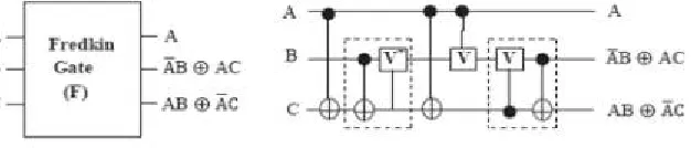
FREDKIN GATE
Reversible 3*3 gate maps inputs (A, B, C) to outputs (P=A, Q=A'B+AC, R=AB+A'C) having Quantum cost of 5 and it requires two dotted rectangles, is equivalent to a 2*2 Feynman gate with Quantum cost of each dotted rectangle is 1, 1 V and 2 CNOT gates. [9]. Fig. 3 shows Fredkin gate.
Fig.3 Fredkin Gate
PERES GATE
Fig.4 Peres Gate
BKG Reversible Gate
BKG Gate [14] is 4*4 novel reversible gate as depicted in Fig. The input vector is represented by T (A, B, C, D) and the output vector is indicated as 0 (P, Q, R, S). Fig. 5 shows BKG Gate.
Fig. 5 BKG Gate
III.PROPOSED ARITHMETIC UNIT DESIGN
The full adder circuit’s output is given by the following equations:
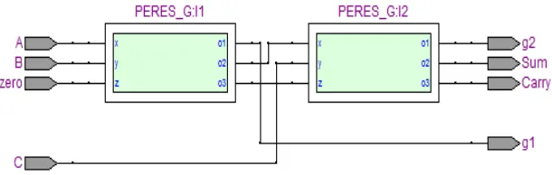
Realization of Reversible Full Adder using Peres Gate is shown in Fig. 6 Full adder is realized with two Peres Gates, which has one constant input and two garbage output [11-13].
Fig. 6 Full Adder using Peres Gates
Fig. 7 shows RTL diagram of Peres Gate Full adder implementation in QUARTUS II 9.1 using VHDL code.
Fig. 7 Synthesis of Full adder using two Peres gate QUARTUS II 9.1
Fig. 8 BKG gate as Full adder
In the first design One Bit Arithmetic Unit is implemented with Fredkin reversible gate as control unit and Peres reversible gate as full adder. As seen in Fig.10 combination of Fredkin Gate and Peres gate is used to perform Arithmetic operation. There is only one constant input to Peres Gate Full Adder, there are four garbage output two from Fredkin Gate and two from Peres Gate as Full Adder.
Fig. 9 Design 1 ALU with Fredkin Gate and Peres Gate as Full Adder
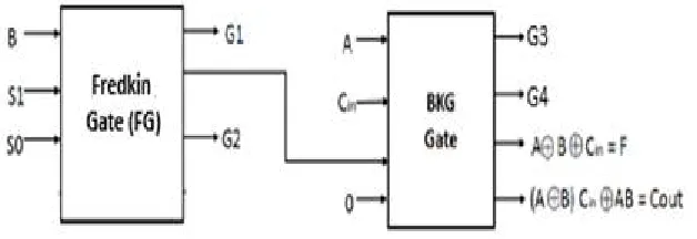
In the second design One Bit Arithmetic Unit is implemented with Fredlkin reversible gate as control unit and BKGs reversible gate as full adder. As seen in Fig.10 combination of Fredkin Gate and BKG Gate is used to perform arithmetic operation. There is one constant input to BKG Gate Full Adder there are four garbage output two from Fredkin Gate and two from BKG gate.
Fig.10 Design 2 ALU with Fredkin Gate and BKG Gate as Full Adder
TABLE I: Function Table for the ALU
Function P equals Output (F) Equals
Function S1 S0 Cin
0 0 0 0 A Transfer A
0 0 1 0 A +1 Increment A
0 1 0 B A + B Add B to A
0 1 1 B A+B+1 Add B to A plus 1
1 0 0 B’ A+ B’ Add 1’s complement of B to A
1 0 1 B’ A+B’+1 Add 2’s Complement of B to A
1 1 0 1 A-1 Decrement A
1 1 1 1 A Transfer A
IV. SIMULATION AND RESULTS
Fig. 11 shows RTL implementation of Arithmetic Unit Design 1, Fredkin gate with Peres gate.
Fig.11 RTL Diagram of Design 1
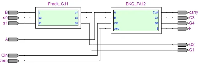
Fig. 12 shows RTL implementation of Arithmetic Unit Design 1, Fredkin gate with BKG gate.
Fig.12 RTL Diagram of Design 2
Fig.12 Simulation waveform for S1 S0 as 00
As seen in Fig. 12 when select input S1 S0 are 00, A is transferred to output when Cin is 0 ad When Cin is 1 the output is A+1.
Fig.13 Simulation waveform for S1 S0 as 01
As seen in Fig. 13 when select input S1 S0 are 01, Output is equal to A+B, when Cin is 0 and when Cin is 1 output is A+B+1.
Fig.14 Simulation waveform for S1 S0 as 10
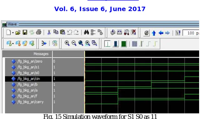
Fig. 15 Simulation waveform for S1 S0 as 11
As seen in Fig. 15 when select input S1 S0 are 11, Output is equal to A-1, when Cin is 0 and when Cin is 1 output is A.
Table II shows the comparison of two proposed design on the basis of Gate count, Garbage output and Number of constant input. Both designs require single constant input as zero, and the number of Garbage outputs are 4. Design 1
require 3 gates and Design 2 requires 2 gates.
TABLE II Parameters of 1-bit Arithmetic Unit
Parameter to be compared
Proposed Design 1 Proposed Design 2
Gate Count
3
2
Garbage Output
4
4
Constant Input
1
1
V. CONCLUSION
In this paper an optimized 1-bit arithmetic Unit to perform 8 different operations has been proposed using two different design. The proposed designs are being implemented using VHDL in QUARTUS II 9.1 and simulation waveform for Arithmetic Unit (using QUARTUS II 9. Modelsim) are shown. The proposed design can be extended to perform different logical operation and Arithmetic and logic Unit (ALU) can be designed
REFERENCES
[1] K. R. Chowdhury, M. Di Felice, “Search: a routing protocol for mobile cognitive radio ad hoc networks,” Computer Communication Journal, vol. 32, no. 18, pp. 1983-1997, Dec.20
[2] K. M. Passino, “Biomimicry of bacterial foraging for distributed optimization,” IEEE Control Systems Magazine, vol. 22, no. 3, pp. 52-67, 2002. [3] Q. Wang, H. Zheng, “Route and spectrum selection in dynamic spectrum networks,” in Proc. IEEE CCNC 2006, pp. 625-629, Feb. 2006. [4] R. Chen et al., “Toward Secure Distributed Spectrum Sensing in Cognitive Radio Networks,” IEEE Commun. Mag., vol. 46,pp. 50–55, Apr. 2008. [5] H. Khalife, N. Malouch, S. Fdida, “Multihop cognitive radio networks: to route or not to route,” IEEE Network, vol. 23, no. 4, pp. 20-25, 2009. [6] Y.-C. Liang et al., “Sensing-Throughput Trade-off for Cognitive Radio Networks,” IEEE Trans. Wireless Commun., vol. 7, pp. 1326–37, April 2008. [7] P. K. Visscher, “How Self-Organization Evolves,” Nature, vol. 421, pp. 799–800 Feb.2003.