638 | P a g e
Structural and Optical Properties of Cu
2+
doped CdO
Nanoparticles
Chitra Bhukkal
1, Rachna Ahlawat
21,2
Material Science Lab.,Department of Physics,
Chaudhary Devi Lal University Sirsa , Haryana, (India)
ABSTRACT
In this work, a direct precipitation method using wet chemical reaction was used to synthesis doped CdO
nanoparticles. Copper doped CdO nanopowder was prepared by wet chemical method at room temperature. The
morphological investigations were carried out by complementary techniques like XRD and FTIR. Optical
properties of the Cu2+: CdO nanoparticles were determined by UV-Vis spectroscopy and band gap energy etc.
The particle size was calculated by well known Debye-Scherrer formula. FTIR analysis revealed the composition
of prepared nanomaterials and threw light on present group of precursors. The optical band gap of Cu doped
CdO is 3.75eV as a result of Cu content. The influence of doping on the band gap energy of CdO nanoparticles
has been examined which was calculated by Tauc’s plot.
I.INTRODUCTION
Metal oxide semiconductor materials have attracted much attraction due to their application in various fields
ranging from electronic devices such as display solar cell, thin film transistor, gas sensor, photo detector and
photodiode [1-3]. There are several synthesis methods to prepare CdO nanoparticles doped with different metals
(Mn,Cu,Co,Al,Ag etc) such as pulsed laser deposition, thermal evaporation, chemical vapor deposition, chemical
bath deposition, sol–gel, and successive ionic layer adsorption and reaction (SILAR) and co-precipitation method
[3-4]. Among these methods co-precipitation method has many advantages such as simple and cheap, simple
experimental setup and possibility of large area deposition. Therefore, in the present work, a considerable
attention has been paid to Cu ion doped CdO for its wide range of applications in optoelectronics like transparent
conducting oxide, solar cell, smart windows, optical communication, flat panel display, photo transistor [5-6], as
well as other type of applications like IR heat mirror, gas sensors, low-emissive and window etc. [7].
Considering various application of CdO nanostructures in different optoelectronics devices, we have attempted to
synthesize the present material to control the optical band gap and structural properties of CdO by doping of
639 | P a g e
II.EXPERIMENTAL DETAIL
2.1 Sample preparation
Cadmium Acetate Dihydrated (Cd(CH3COO)2.2H2O) about 0.2 M and Sodium Hydroxide (NaOH) about
0.075M were taken according to their molar ratio in a beaker and stirred about an hour at a room temperature. In
an another beaker Copper Acetate Monohydrate (C4H6 CuO4.4H2O) were taken and dissolved in 100 ml of
double distilled water at room temperature and stir for half an hour. The solution of second beaker was added
drop wise in the first beaker. The color of the solution changes white to the yellowish brown during the reaction.
After completion of the stirring, the precipitates were left undisturbed for 1 day and then washed and filtered.
Then the precipitates were dried in air oven at a temperature 120◦C for 5 hours.
2.2 Characterizations
The prepared sample was characterized by well-known techniques like XRD, FTIR, and Uv-Vis spectroscopy.
The x-ray diffract grams were taken with the help of XPERT-PRO x-ray diffractometer operated at 45 kV and 40
mA, using monochromatic Cu Kα radiation of wavelength 1.5406 Å in the different 2o ranges. FTIR spectrum of
the prepared nanostructure was taken at room temperature using Perkin Elmer 400 spectrophotometer in the
400-4000 cm-1 range. The optical absorption spectra have been observed by using Lambda 750 (Perkin Elmer) UV-Vis-NIR spectrophotometer in 200-800 nm range.
III.RESULTS AND DISCUSSIONS
3.1- X -Ray Diffraction (XRD) Analysis
Powder X-ray diffraction pattern of Cu doped CdO nanostructure is shown in fig 3.1. In the prepared product,
several diffraction peaks are appeared. The most intense diffraction peak appeared at 30.18◦, 36.11◦, 49.74◦, 57.9◦, 61.50◦ with miller indices (111), (200), (220), (311), (222) indices for the cubic symmetry of CdO nanocrystals. Diffraction peaks observed were matched with standard JCPDS DATA (05-0640) and lattice parameters were
calculated using the matched (hkl) values. In addition, Peaks at 2θ ~ 23.36◦, 43.58◦, 74.9◦ corresponds to the unreacted cadmium hydroxide [8] and represent unknown phases. The existence of sharp peaks in the XRD
spectra confirms the crystalline nature of the prepared material and broadening of diffraction peaks in the sample
confirms the formation of nanoparticles specially the quantum dots. The crystalline size (D) of the prepared
sample was calculated from Scherrer’s equation. The average crystalline size of the Cu doped nanostructure is
found to be ~ 16.88 nm.
Crystallite Size (D) =
(1)
Where, λ is the wavelength of the radiation, β is the full width half maximum (FWHM) and θ is the Bragg
640 | P a g e
and FWHM of the sample represent a change in crystalline size due to the differences between the ionic radii ofthe dopant and host material.
20 30 40 50 60 70 80
500 1000 1500 2000 2500 3000
Inte
nsi
ty
(a.
u.)
S2 (CdO: Cu)
2 theta (in degree)
Figure 3.1: XRD of as prepared sample of Cu doped CdO.
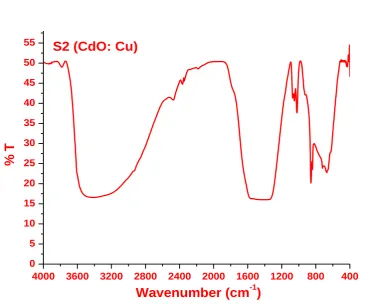
3.2Fourier Transform Infrared (FTIR) Spectroscopy:
Fig. 3.2 shows IR Spectrum of Cu doped CdO nanoparticles. In FTIR spectra 3580-3515cm-1 are attributed to the stretching and bending vibration of the absorbed water molecule in the sample [9].
TABLE 1
Wave number (cm-1) Group
3401 = attributed to stretching and bending vibration of the absorbed water molecule [9].
2476 = assigned to asymmetric stretching vibrations of CH2 group [10].
2366 = attributed to O= C=O vibration absorbed from environment on the metallic cation [10].
2173 = attributed to asymmetric vibration of acetate complex (COO-) [10].
1371 = attributed to symmetric vibration of acetate complex (COO-) [10].
1071 = present due to formation of C-OH complex
1051 = C-O bonding vibration
925 = bending vibrations of the COO- group
857 = attributed to CO32- (carbonate) groups [11].
670 = may be assigned to Cd-OH bond present in the complex [11].
641 | P a g e
4000 3600 3200 2800 2400 2000 1600 1200 800 400
0 5 10 15 20 25 30 35 40 45 50
55
S2 (CdO: Cu)
%
T
Wavenumber (cm
-1)
Fig. 3.2: FTIR of as prepared sample of Cu doped CdO.
3.3
Optical Absorption & Band Gap Energy
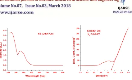
The optical properties and the band gap energy of the Cu doped nanostructure are studied by UV-Vis absorption
spectroscopy. The optical absorption to the prepared sample is investigated in the wavelength range 200-800 nm
and is presented in Fig. 3.3 (a). The absorbance differs depending upon the several factors like particle size,
oxygen deficiency and defect in grain structure. For the synthesized nanostructure a strong and broad optical
absorption band is obtained between 350 nm and 550 nm. From the spectrum, it is clear that the strong
absorbance is found for wavelength in the visible region. Also, the absorption edge of the prepared nano- powder
is found to shift towards the high energy (means lower wavelength region) when compared to pure CdO [12-13].
The band gap of semiconductor changes as the dopant can cause crystal defects. The band gap increases with
dopant presence which may be caused by defects or crystalline size. The CdO sample is known to be a
642 | P a g e
200 300 400 500 600 700 800 900
0.0 0.5 1.0 1.5 2.0 2.5 3.0 3.5 4.0
S2 (CdO: Cu)
In tens ity (a. u.) Wavelength (nm)
1.5 2.0 2.5 3.0 3.5 4.0 4.5 5.0
0 50 100 150 200 250 300 350 [abs . Coe ff. x Ene rgy ] 2 Energy (eV) S2 (CdO: Cu)
Eg = 3.75 eV
Figure 3.3 (a): Absorption spectrum (b) Tauc’s Plot of Cu doped CdO
The relation between the incident photon energy (hν) and the absorption coefficient (α) is given by the following
equation:
(αhν)1/n= A (hν-Eg)
(2)
Here, A is a constant, α is absorption coefficient and Eg is the band gap energy of the material and the exponent n
depends on the type of transition. For direct allowed transition n = 1/2, for indirect allowed transition n= 2, for
direct forbidden n= 3/2 and for indirect forbidden n= 3. Direct band gap of the samples are calculated by plotting
(αhν)2 verses hν and then extrapolating the straight portion of the curve on hν axis at α = 0 as shown in the Fig. 3.3 (b). The optical band gap of the sample is calculated as 3.75 eV which is higher value when compared to
undoped CdO (~2 - 2.5eV) from literature. For the Cu doped CdO nanostructure, band gap value considerably
with the change of doping materials. It may be based on Moss-Burstein (MB) where the dopant ion can lead to a
change in free electron density in the conduction band which shift the Fermi level in this way change the band
gap properties [14]. Also, few researchers reported that occupation of interstitial position in the crystalline
structure lead to a band gap widening [15-16]. It is examined that this alteration in the band gap energy could be
because of change in crystalline size of the prepared nanostructure. This observation confirms that the well
known quantum size effect which lead to the enlargement of band gap energy at small crystalline sizes.
IV.CONCLUSIONS
Cu doped CdO nanostructure has been successfully synthesized via the chemical precipitation method. The
present study, confirmed that the chemical precipitation method is an easy and cost effective technique for
synthesis of nanoparticles in a large scale. XRD study reveals that CdO nanoparticles are nanocrystalline cubic
643 | P a g e
using well known Debye-Scherrer formula. In FTIR spectrum, it is demonstrated that the Cd-OH band is presentat 670 cm-1 and Cd-O band is present at 413cm-1. Most intense and deep band present at 3401 cm-1 and 1371 cm-1 revealed the large amount of hydroxyl and acetate groups present due to precursors. A broad band of absorbance
is investigated in the visible region (~350-530 nm) using uv- visible spectroscopy. The band gap energy was
calculated ~3.75 eV using famous Tauc’s Plot. We expect that this type of nanostructures might be interest for
application in solar energy converter and photo catalytically reactors.
REFERENCES
[1] Y.R. Suia, Y. G.Yuea, Y. P. Songa, B. Yaob, et al. , Ceramics International, vol. 41, 2015, 5414–5420.
[2] L. T. Jule, F. B. Dejene, A. G. Ali, Journal of Alloys and Compounds, 687, 2016, 920-926.
[3] S. G.Niyaky, M. Montazerozohori, A. Masoudiasl, J.M. White, J. Mol. Struct. 1131, 2017,201–211.
[4] N.B. Sonawane, P.K. Baviskar, R.R. Ahire, B.R. Sankapal, Mater. Chem. Phys. 191, 2017, 168–172.
[5] A. Fakhri, S. Behrouz, M. Pourmand, J. Photochem. Photobiol. B, 149, 2015, 45-49.
[6] N. Thovhogi, E. Park, E. Manikandan, M. Maaza, A. Gurib-Fakim, J. Alloys Comp.655, 2016, 314–320.
[7] A. Fakhri, R. Khakpour, J. Lumin. 160, 2015, 233–237.
[8] Volkan Eskizeybek, Okan Demir, Ahmet Avei, Manish Chhowalla, 13, 2011, 4673-4680.
[9] Mergoramadhayenty Mukhtar, Lusitra Munisa, Rosari Saleh, Material Science and Application, 3, 2012,
543-551.
[10] S. Sivakumar, A. Venkatesan, P. Soundhirarajan, Chandra Prasad Khatiwada, Spectrochimica Acta Part
A:Molecular and Biomolcular Spectroscopy, 136, 2015, 1751-1759.
[11] G.Thirumala Rao,B. Babu, R.Joyce Stella, V. Pushpa Manjari, R.V.S.S.N. Ravikumar, Spectrochimica Acta
Part A: Molecular and Biomolecular Spectroscopy, 139, 2015 , 86-93.
[12] A.A. Dakhel, Sol. Energy 83, 2009, 934–939.
[13] S. Kose, F. Atay, V. Bilgin, I. Akyuz, Int. J. Hydrog. Energy , 3452, 2009, 60–52.
[14] M. Benhaliliba,C.E. Benouis, A. Tiburcio, F. Yakuphanoglu, Journal of Luminescence, 132, 2012,
2653-2658.
[15] K. Anandhan, R. Thilak Kumar, Spectrochimica Acta Part A: Molecular and Biomolecular Spectroscopy,
149, 2015, 476-480.
[16] R.K.Gupta, Z. Serbetci, F. Yakuphanoglu, Journal of Alloys and Compounds, 515, 2012, 96-100.