IJEDR1503070
International Journal of Engineering Development and Research (www.ijedr.org)1
with sleep insertion technique is one of the efficient technique for designing combinational digital circuits which significantly cuts down the leakage current without increasing the dynamic power dissipation, sleep insertion technique is also added along with variable body biasing technique so that there is no loss of state as in sleep stack technique. This thesis proposed a technique that reduces both power dissipation and glitches. This technique is based on two methods first is variable body biasing and the other is sleep insertion technique. Pass transistor is also added in the circuitry in order to eliminate glitches if any. The existing leakage reduction techniques like sleepy keeper and stack technique are having drawbacks like increased area and delay. Other delay elements that are used for reduction in glitches takes larger area when compared with pass transistor. This new proposed approach eliminates leakage power along with glitches keeping in mind all the drawbacks of all the earlier techniques. All the performance has been investigated using 90nm Technology at 1 voltage and evaluated by the comparison of the simulation result obtain from TSPICE.Keywords - VBBT, Delay, leakage power, sleep insertion technique
________________________________________________________________________________________________________
I. INTRODUCTION
Complementary metal oxide semiconductor (CMOS) technology is used in all modern digital logic circuits. The power spent in CMOS can be classified as dynamic power consumption and leakage or static power consumption. Dynamic power consumption is due to the low impedance path between the rails formed through the switching devices. When input is given to the gate, there would be occurrence of one or more transitions at the output. At the output of the gate there are two types of transitions occurs, one which is due to actual transmission of the input signal resulting in desired functioning of the logic gate, is also called as functional transition Second, is due to transmission of unnecessary pulses through the logic gate resulting in undesired functioning of the gate, this is called as spurious transition. These spurious transition at the output of a logic gate is an outcome of difference in arrival time of various inputs. These unnecessary signals at the output of logic gate are known as glitches. Glitch power in modern circuits account for 20 to 70% [1] and it is 7 to 43% [2] of the dynamic power consumption. There are various published techniques to eliminate glitches in the logic circuits to accompany desired functioning of the logic circuit.
However, low-power design usually involves making tradeoffs such as timing versus power and area versus power. Increasing performance, while the power dissipation is kept constant, is also considered to be a low-power design problem. In fact, higher performance-per-watt is the new technique for micro-processor chip manufacturers today. In order to achieve high density and high performance, CMOS technology feature size and threshold voltage have been scaling down for decades. Because of this trend, transistor leakage power has increased exponentially. The reduction of the supply voltage is dictated by the need to maintain the electric field constant on the ever shrinking gate oxide.
II. CONVENTIONAL FULL ADDER
IJEDR1503070
International Journal of Engineering Development and Research (www.ijedr.org)2
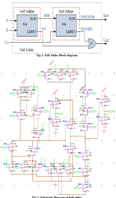
Fig 1: Full Adder Block diagramIJEDR1503070
International Journal of Engineering Development and Research (www.ijedr.org)3
Fig 3: Waveform of the Schematic diagram of Conventional Full AdderIII FULL ADDER IMPLEMENTATION USING VARIABLE BODY BIASING WITH SLEEP INSERTION TECHNIQUE Proposed VBBT with Sleep insertion Technique
This new sleep variable body biasing technique reduces both leakage power and glitch in the logic circuit. This design includes both-
(i)Variable body biasing and (ii)Sleep insertion technique
Sleep insertion technique is a state destructive technique that cuts off either pull-up or pull-down or both the networks from the supply voltage or ground or both using sleep transistors. This technique is an extension to MTCMOS, which adds down networks and ground while for fast switching speeds, low-vth transistors are used in logic circuits, this process reduces leakage power during sleep mode.
The source of one of the sleep transistor is connected to the body of other sleep transistor in order to have a variable body biasing effect. Due to this connection the threshold voltage of the sleep transistors increases due to variable body biasing during sleep mode.
Figure 1 Variable Body Biasing with Sleep Insertion Technique
Application of VBBT along with sleep insertion technique on Full Adder to calculate the amount of leakage power reduced in VBBT technique.
IJEDR1503070
International Journal of Engineering Development and Research (www.ijedr.org)4
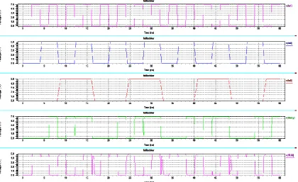
Fig 5: Schematic Diagram of Full Adder Implemented by using Variable Body Biasing with sleep insertion techniqueThe VBBT based Full Adder is shown in Figure5 with the two transistors used as variable body biasing and one transistor is added in order to add stack approach so that the disadvantage of state destructive stage is overcome. The simulation waveforms of VBBT AND gate from Figure4 show that the basic characteristics of AND are retained by VBBT AND gate.
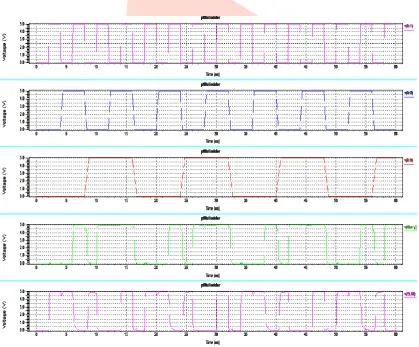
Fig 6:Waveform of Schematic diagram of Full Adder implemented along with Variable Body Biasing with Sleep Insertion Technique
IJEDR1503070
International Journal of Engineering Development and Research (www.ijedr.org)5
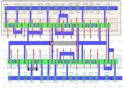
Fig 7:Layout of Full Adder Implemented by using Variable Body Biasing with Sleep Insertion TechniqueV EXPERIMENTAL RESULTS
The leakage power is measured using the Tanner Tool S-EDIT simulator. The results obtained through the technique for Full Adder are shown in Table 1. Simulation for Full Adder are performed by taking process parameter, 90nm CMOS Technology.
Table-1
Gate Type Glitch % Power consumption(pw) %age reduction in power consumption Conventional VBBT Conventional VBBT
FULL ADDER 40 0 7.29 6 20
VI.CONCLUSION
In this paper we have presented leakage power reduction VBBT technique along with sleep insertion technique. It becomes a great challenge to tackle the problem of leakage power. In this technique two individual techniques are combined one is sleep insertion technique and the other is variable body biasing technique. VBBT achieves the reduction in leakage power compared to other leakage reduction techniques, such as sleep transistor, sleepy keeper, etc. The performance has been investigated using 90nm Technology and evaluated by the comparison table 1 of the simulation result obtain from TSPICE.
REFERENCES
[1] A..Shen,A.Ghosh,S.Devadas and K.Keutzer, “On average power dissipation and random pattern testability of CMOS combinational logic networks,”proc. ICCAD,pp.402-407,1992.
[2] D.Brad and C.Vishweshwaraiah, “Inaccuracies in power estimation during logic synthesis,” proc. ICCAD,pp.388-394,1996. [3] M. D. Powell, S. H. Yang, B. Falsafi, K. Roy, and T. N. Vijaykumar, “Gated-Vdd: A circuit technique to reduce leakage in deep submicron cache memories,” in Proc. IEEE ISLPED, 2000, pp. 90-95.
[4] Tezaswi Raja and Michael L. Bushnell ,” Variable Input Delay CMOS Logic for Low Power Design”. .IEEE Transcations on very large scale integration (VLSI) systems Vol 17. No. 10. October 2009.
[5] Sarvesh Bhardwaj and Sarma Vrudhula .” Leakage Minimization of Digital Circuits Using Gate Sizing in the Presence of Process Variations ”.IEEE Transactions on computer –aided design of integrated circuits and systems. Vol. 27. No. 3 , March 2008.
[6] M. Powell, S.-H. Yang, B. Falsafi, K. Roy and T. N. Vijaykumar, “Gated-Vdd: A Circuit Techniqueto Reduce Leakage in Deep submicron Cache Memories,” International Symposium on Low Power
Electronics and Design, July 2000, pp. 90-95.
[7] Yuanlin Lu and Vishwani D. Agrawal “CMOS Leakage and Glitch minimization for power performance tradeoff ” Department of Electrical and Computer Engineering, Auburn University, Auburn, AL 36849, USA. Journal of Low Power Electronics vol. 2, 1-10, 2006.
IJEDR1503070
International Journal of Engineering Development and Research (www.ijedr.org)6
[9] Bagadi Madhavi, G Kanchana, Venkatesh Seerapu “Low Power and Area Efficient Design of VLSI Circuits” International Journal of Scientific and Research Publications, Volume 3, Issue 4, April 2013, ISSN 2250-3153.[10] B. S. Deepak subramanyan and A. Nunez, “Analysis of Sub threshold Leakage Reduction in CMOS Digital Circuits,” Proceedings of the 13th NASA VLSI Symposium, Post Falls, 5-6 June 2007, pp. 1-8.
[11] R. X. Gu and M. I. Elmasry, “Power Dissipation Analysis and Optimization of Deep Submicron CMOS Digital Circuits” IEEE Journal of Solid-State Circuits, Vol. 31, No. 5, 1996, pp. 707-713. http://dx.doi.org/10.1109/4.509853.
[12] Y.Taur, T.H. Ning, “Fundamentals of Modern VLSI Devices”, Cambridge University Press, New York, 1998.
[13] International Technology Roadmap for Semiconductor (ITRS-05). http://www.itrs.net/ Links/ 2005ITRS/Design2005.pdf. [14] D. Lee, W. Kwong, D. Blaauw and D. Sylvester, “Analysis and Minimization Techniques for Total Leakage considering Gate Oxide Leakage" In Proceedings of the 40th Design Automation Conference, pp. 175-180, Anaheim, 2003.
[15] P. Verma, R. A. Mishra, “Leakage power and delay analysis of LECTOR based CMOS circuits”, Int’l conf. on computer & communication technology ICCCT 2011.