Design and Implementation of a Low Power Second
Order Sigma-Delta ADC
K. Lokesh Krishna1, M. Jagadeesh 2, T.Ramashri3, K.Anuradha4
AssociateProfessor, Department of ECE, S.V.C.E.T.,Chittoor, Andhra Pradesh, India. PG Student, Department of ECE, S.V.C.E.T.,Chittoor, Andhra Pradesh, India.
Professor, Department of ECE, S.V.U.C.E.,Tirupati, Andhra Pradesh, India. Professor, Department of CSE, L.B.C.E.W.,Visakhapatnam, Andhra Pradesh, India.
Abstract— Sigma-Delta (∑-∆) analog to digital converters are
well known for its use in high accuracy wireless communication applications. It is alternative for low power, high resolution (greater than 12 bits) converters, which can be ultimately integrated on digital signal Processor ICs. In this work Over Sampling concept is used to address the problem of power dissipation and noise in ADCs. In this paper a Second order Sigma-Delta Modulator is implemented using CMOS 0.13μm technology using a 1.2 V power supply. Over sampling ratio are 128 with clock frequency of 5 GHz which gives bandwidth of 20 GHz. The total power dissipation of the modulator is 0.87mW. The area occupied by the modulator is 30µm×35µm.
Keywords— Analog to Digital Converter, Sigma-Delta, Low
Power, Digital to Analog converter, Oversampling, Quantizer, Summer.
I. INTRODUCTION
In modern wireless communication system design there is a huge demand for larger bandwidths and operating at high speeds. Also in recent years, the wireless portable products have become more and more popular in our day to day activities. To achieve these specifications Analog to Digital Converters (ADCs) plays an important role in high speed wireless communication. So there is a huge demand for Analog to Digital Converters from the past decade. ADCs are generally needed to link the analog and digital domains. There are numerous applications such as Wireless Telecommunications, Medical Imaging, Audio and Video Processing Systems, Instrumentation and Digital Radio Systems where ADCs are very important. In general there are a number of ADC architectures such as Flash type, Sigma Delta, Folding, Subranging, Successive Approximation Register type and Pipelined available to meet these applications. But selection of an ADC depends upon the application and its specifications. However no single ADC architecture is suitable for all the applications [1] - [7]. Of these, sampling rate in excess of 600 MHz and bit resolution of more than 12 bits are increasingly required to accommodate the very large bandwidth required in many wireless applications. The ∑Δ modulator offers a solution to achieve high resolution data conversion while still maintaining better speed. Compared with Nyquist- rate ADCs, Oversampling
ADCs use more digital signal processing functions to perform analog to digital conversion. [8]. Also Oversampling ∑Δ
ADCs do not need steep roll-off anti-alias filtering which is usually required in Nyquist-rate ADCs. Sigma Delta modulation is a robust means of implementing high-resolution analog to digital converters in mixed signal designs [9]-[12]. In this paper a second order ∑Δ ADC is proposed for 1.2V supply using 0.180µm CMOS technology. The designed ADC achieves high resolution, low power consumption and better speed.
The outline of the work is as follows. Section II discusses about the analog to digital converter. Section III discusses about the Sigma-Delta architecture and Section IV presents design of various sub-blocks associated with the modulator and its results. Section V is conclusion.
II. ANALOG TO DIGITAL CONVERTER
Data converters are recognized as converting the one form of input signal into another form of signal. The Figure 1, shows the simple block diagram of analog to digital converter which has analog signal as input and gives digital output.
Fig. 1. Block diagram of Analog to Digital Converter
ADCs are distinguished mainly as two types, such as (i) Nyquist-Rate Converters and (ii) Oversampling converters.
reconstruction filters. In most cases, Nyquist rate converters operate at 1.5 to 10 times the Nyquist rate.
Oversampling converters are those converters which operate much faster than the input signal’s Nyquist rate (typically 20 to 512 times faster) and increase the output’s signal-to-noise ratio (SNR) by filtering out quantization noise that is not in the signal’s bandwidth. In A/D converters, this filtering is performed digitally, whereas in D/A converters, analog filter is used. Most often, oversampling converters use noise shaping to place much of the quantization noise outside the input signal’s bandwidth [13].
In oversampled ADCs, an analog signal is sampled and quantized at a sampling frequency higher than the Nyquist rate, and then the quantization noise from the quantizer will spread through the spectrum uniformly. A higher sampling rate will result in a lower quantization noise power in the signal bandwidth and consequently a higher bit resolution can be achieved. Using a digital low-pass filter (LPF), the out-of-band quantization noise can be filtered and finally the signal is down-sampled to the Nyquist rate. The delta-sigma ADC is the main form of oversampling ADCs. By using a feedback loop in the modulator, the quantization noise is shaped to further reduce the quantization noise power in the signal bandwidth. Oversampling allows noise filtering to be done in the digital domain but at higher frequency.
III.SIGMA-DELTA (∑-∆) MODULATOR ADC ARCHITECTURE
Sigma Delta (∑-∆) modulators are the most suitable Analog-to-Digital Converter (ADC) topologies for digitizing with high-resolution analog signals characterized by a bandwidth much smaller than the sampling frequency fs. With
these architectures, a resolution up to 19–21 bits can be reached using standard Integrated Circuit (IC) technologies. Sigma delta modulators employ coarse quantization enclosed in one or more feedback loops. Sigma delta modulators are generally known as noise shaping modulators due to their quantization noise association with a differential function that shapes the noise frequency spectrum.
The differential function suppresses in-band frequency components of the quantization noise. The order of a modulator is determined by the differential function order. A higher order modulator has a higher differential function order, which further suppresses the in band quantization noise. The differential function makes sigma delta modulation ADC achieves high resolution than those conventional ADCs when sampling rates are increased.
The sigma-delta modulator architecture is implemented by combining two summing integrators with comparator and 1-bit D/A converter, as shown in Figure 2. The most important building block in this architecture is an integrator, for which the output is the delayed integration of a weighted sum of input. The remaining building blocks in the analog portion of the modulator are comparator and 1-bit D/A converter. The comparator circuit acts as a 1-bit A/D converter that maps its input into one of two digital output codes. The two digital output codes are then mapped back into analog levels by the D/A converter. X represents input signal, Y represents sampled output, y represents feedback input and gn represents
gain.
IV.DESIGN OF SUB-BLOCKS AND ITS RESULTS
All required analog blocks (operational amplifiers, switches, sample and hold circuit and quantizer) were designed, simulated and then layout is carried out.
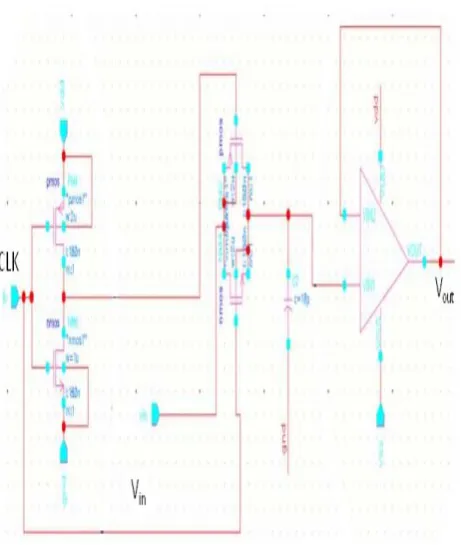
A. Sample and Hold circuit:
Sample and hold circuit is an important analog building block in many applications. The function of the sample and hold circuit is to sample an analog input signal and hold this value over a certain length of time for sub sequent processing. The input to the sample and hold circuit is a sine wave having amplitude of 1.2Vp-p, power supply is ±0.6V, and clock
frequency is 10GHz. Here input signal is sampled based on the clock frequency. The width of the transistors are set as NMOS=1µ, PMOS = 2µ and capacitor value is 1uF. To avoid loading effect, a Voltage follower circuit is connected at the output side. Figure 2 shows the schematic diagram of sample and hold circuit.
B. Operational Amplifier:
Figure 5 shows the schematic diagram of operational amplifier [15]-[16] for implementing integrator circuit and Figure 6 shows the simulated results of the operational amplifier.
Fig. 3. Schematic diagram of Sample and Hold circuit
Figure 4 shows the simulation results of sample and hold circuit.
Fig. 4. Simulation results of Sample and Hold circuit
Fig. 5. Schematic diagram of Operational Amplifier
C. Comparator circuit:
A Comparator circuit is used for comparing the input voltage with a known reference voltage. If the input voltage is greater than reference voltage, then the comparator output is one, else if the input voltage is less than reference voltage the comparator output is zero. Figure 7 shows the Comparator circuit [14]. Here M1, M2 transistors are differential pair, M6
and M7 transistors provide the necessary gain. Layout has
been drawn and area occupied for designing the comparator is found to be 496.668µm2. Table 1 shows the designed
transistor widths.
Table 1 Widths of transistors used in comparator circuit
Transistor Width(m)
M1 3.4u
M2 3.4u
M3 0.8u
M4 0.8u
M5 0.6u
M6 0.65u
M7 27.5u
M8 27u
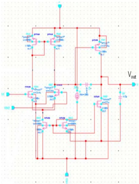
All the sub-blocks are combined together to give final top level schematic of second order sigma delta ADC. Figure 8 shows the top level schematic of the designed ADC.
Fig. 7. Schematic diagram of Comparator circuit
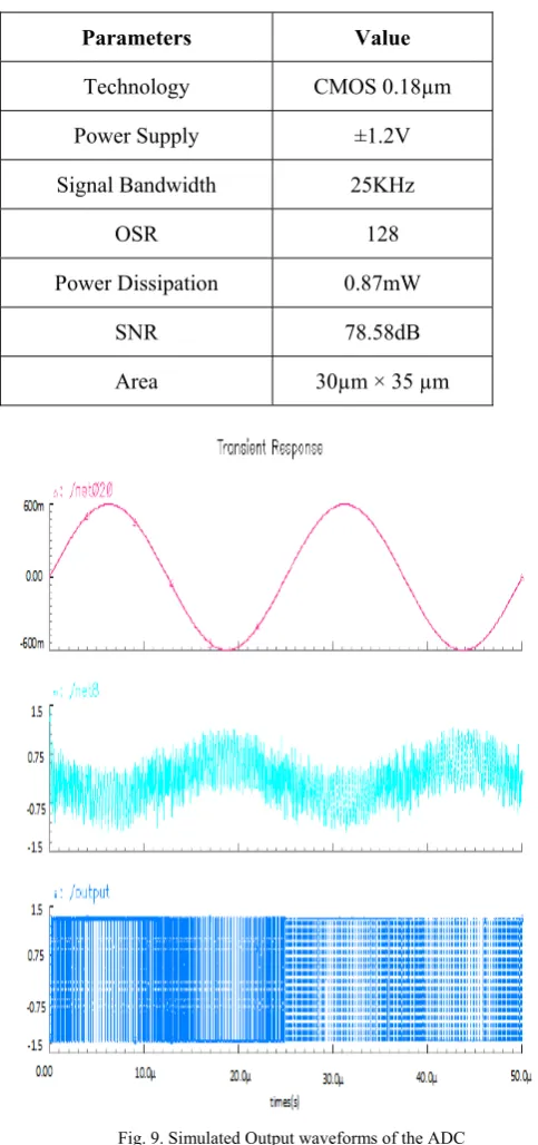
Output spectrum obtained from transistor level simulations data for 1GHz sinusoidal input signal is shown in Figure 9. Input signal frequency is 1GHz, which is enough to have a reasonable simulation time, while giving enough samples (16 k samples) to perform a FFT. The power dissipation of the modulator was found to be 0.87mW. The designed modulator occupies the area of 33mm×45mm.
Table 2 Performance Summary of the ADC
V. CONCLUSION
Sigma-Delta modulation ADCs are used in a wide variety of applications such as wired and wireless communications, medical, instrumentation and automotive electronics. Sigma- Delta modulation based analog to digital conversion technology is a cost effective alternative for low power, high resolution (greater than 12 bits) converters, which can be ultimately integrated on digital signal processor ICs. In this paper over sampling concept is used to address the problem of power dissipation, noise in ADCs and investigating the possibilities of utilizing alternative methods to reduce the noise and power dissipation in ADC architectures. This is achieved by design techniques namely over sampling and second order delta architecture. A second order sigma-delta modulator is implemented using CMOS 0.18μm technology using a 1.2 V power supply. Over sampling ratio are 128 with a clock frequency of 5 GHz which gives bandwidth of 20 GHz. The power dissipation is found to be 0.87mW and power density is found to be 0.140W/ µm2. The
operating frequency can be increased by redesigning the Op-amp to operate at higher bandwidth by changing the bias current and driving capability.
Fig. 9. Simulated Output waveforms of the ADC
REFERENCES
[1] . Jun He, Sanyi Zhan, Degang Chen and Randall L. Geiger, “Analyses of Static and Dynamic Random Offset Voltages in Dynamic Comparators”, IEEE Transactions on circuits and systems , Vol. 56,
No. 5, May 2009.
[2] . Thomas Liechti, Armin Tajalli, Omer Can Akgun, Zeynep Toprak, and Yusuf Leblebici, “A 1.8V 12-bit 230-MS/s Pipeline ADC in 0.18μm CMOS Technology”, IEEE International Conference, 2008.
[3] . A. Varzaghani and C. K. K. Yang, “A 600 MS/s 5-bit pipelined analog- to-digital converter using Digital reference Calibration”,
IEEE Journal of Solid-State Circuits, Vol. 41, No. 2, pp. 1-4, Feb.
2006.
[4] . Yeonseong Hwang and Minkyu Song, “Design of a CMOS Image Sensor Based on a 10-bit Two-Step Single-Slope ADC” Journal of
Semiconductor Technology and Science ,Vol.14, No.2, April, 2014.
[5] Jyun-Syong Lai and Zhi-Ming Lin, “A 6-bit 2GS/s Low Power Flash ADC”, IACSIT International Journal of Engineering and Technology, Vol. 4, No. 4, August 2012.
[6] . Y.J. Kim, Y.J. Cho, D.H. Sa and S.H. Lee.: “A 10 b 200 MS/s 1.8 mm2
83 mW, 0.13 μm CMOS ADC Based on Highly Linear Integrated Capacitors”, IEICE Transactions on Electronics, (2007).
[7] . B. Hernes, J. Bjornsen, T. N. Andersen, A. Vinje, H. Korsvoll, F. Telsto, A. Briskemyr, C. Holdo, O. Moldsvor. “A 92.5mW 205MS/s 10b Pipeline IF ADC implemented in 1.2V/3.3V 0.13um CMOS”,
IEEE Solid- State Circuits Conference Digest of Technical Papers,
pp. (462- 615) (2007).
[8] . Altun, O. Jinseok Koh, Allen, P. E. “A 1.5V Multirate Multibit Sigma Delta Modulator for GSM / WCDMA in a 90nm Digital CMOS Process”, IEEE Conference, Vol. 6, pp. 5577- 5580 (2005).
[9] . Sam Kavusi, Hossein Kakavand, and Abbas El Gamal. “On Incremental Sigma-Delta Modulation with Optimal Filtering”, DARPA Microsystems Technology Office, (2005).
[10] . Eric Fogleman, Jared Welz and Ian Galton. “An Audio ADC Delta– Sigma Modulator with 100-dB Peak SINAD and 102-dB DR using a Second-Order Mismatch-Shaping DAC”, IEEE Journal of Solid-State Circuits, Vol. 36, No. 3, pp. 339-348 (2001).
[11] . Reddy, K. ; Rao, S. ; Inti, R. ; Young, B. ; Elshazly, A. ;Talegaon kar.M, ; Hanumolu, P.K., “A 16-mW 78-dB SNDR 10MHz BW CT Sigma-
Delta ADC Using Residue-Cancelling VCO Based Quantizerr”, IEEE Journal of Solid State Circuits, Vol. 47, Issue Parameters Value
Technology CMOS 0.18µm
Power Supply ±1.2V
Signal Bandwidth 25KHz
OSR 128
Power Dissipation 0.87mW
SNR 78.58dB
No:12, pp. (2916 – 2927), 2012.
[12]. Zaliasl, S. ; Saxena, S. ; Hanumolu, P.K. ; Mayaram, K. ; Fiez, T.S., "A 12.5 bit 4MHz 13.8mW MASH Sigma Delta Modulator With Multirated VCO-Based ADC ”, IEEE Transactions on Circuits and
Systems 1:Regular Papers, Vol. 59, Issue No:8, pp. (1604 – 1613),
2012.
[13] . Tony Chan Carusone, David A.Johns. and Kenneth W.Martin “ Analog Integrated Circuit Design” John Wiley & Sons, Inc. Second Edition, NJ (2012).
[14] . Dragisa Milovanovic, Milan Savic, Miljan Nikolic, “Second Order Sigma-Delta Modulator in Standard CMOS Technology”, Serbian
Journal of Electrical Engineering, Vol.1, No.3 pp. 17-20 (2004).
[15]. Phillip E.Allen and Douglas.R. Holberg. “CMOS Analog Circuit
Design”, Oxford University Press, Second edition (2002).
[16} . R.Jacob Baker “CMOS Mixed Signal Circuit Design”, IEEE Press

![Fig. 2. Second Order Sigma-Delta Modulator Architecture [14]](https://thumb-us.123doks.com/thumbv2/123dok_us/7841236.1299735/2.595.96.537.564.675/fig-second-order-sigma-delta-modulator-architecture.webp)