ISSN (Print) : 2320 – 3765 ISSN (Online): 2278 – 8875
I
nternational
J
ournal of
A
dvanced
R
esearch in
E
lectrical,
E
lectronics and
I
nstrumentation
E
ngineering
(A High Impact Factor, Monthly, Peer Reviewed Journal)
Website: www.ijareeie.com
Vol. 7, Issue 3, March 2018
Coupled Inductor based Interleaved Boost
Converter for Enhanced Time Response
V.Rajeswari1, S.Sushmitha1, M.Sumathi1, Bala Vignesh2
B. E Student,Department of EEE, RMK Engineering College, Kavaraipettai, Tamil Nadu, India1 Asst Professor, Department of EEE, RMK Engineering College, Kavaraipettai, Tamil Nadu, India 2
ABSTRACT: Recently, Inter Leaved Boost Converter (ILBC) has been developed as an alternative between the PV system and the load. DC level is increased using a boost regulator. ILBC is utilized to escalate the voltage gain. The objective of the suggested closed loop ILBC system is to enhance the dynamic response of ILBC using FOPID controller. Simulink models are developed for PI and FOPID controlled ILBC systems. The results of PI and FOPID based ILBC systems indicate that the voltage response with FOPID is superior to PI controlled ILBC system.
KEYWORDS: Coupled Inductor - PI Controller-FOPID Controller- MOSFETS - Inter leaved boost Convertor(ILBC) - PIE Filter- PIC MicroController 16F84.
I. INTRODUCTION
Fuel cell stacks and photovoltaic panels generate low DC voltages and these voltages need to be boosted before converted to AC voltage. Therefore, high step-up ratio DC-DC converters are preferred in renewable energy systems. A new topology to boost the input voltage to desired levels with low duty ratios, utilizing coupled inductor and to achieve high step-up voltage gain with an appropriate duty ratio have been proposed [1], [2]. In addition, a passive clamp circuit reduces the voltage stresses on the main switch and Output diode; therefore low resistance RDS (ON) for the main switch can be adapted to reduce conduction loss.
The key factors for renewable energy power conversion systems in industrial applications are Efficiency, power quality, and reliability. Du [3] suggested a novel scheme to improve performances of high-voltage large-capacity photovoltaic power stations. The power conversion of the photovoltaic system is divided into two stages, i.e. DC/DC power conversion and DC/AC power conversion. In DC/DC stage, many power units are connected in parallel, each one of which includes a photovoltaic array and a non-isolated DC/DC converter. The DC/AC power conversion is equivalent to a voltage source in series with a current source. A family of a single-switch three-diode DC-DC Pulse Width Modulated (PWM) converters operating at a constant frequency and a constant duty cycle is presented by Ismail[4]. It’s described that the converters are different from the conventional DC-DC step-up converters, and they possess higher voltage gain with small output voltage ripples.
However, A high step-up converter with high step-up gain and low diode voltage stress, suitable for green power source conversion by employing acoupled inductor and switched capacitor, achieves high step-up conversion ratio without adopting extremely high duty ratio or high turns ratio. The voltage spike that occurs on the power switch is alleviated allowing a low-voltage-rated power switch with low RDS(ON) and thus reduces the conduction losses is presented by Kuo-Ching Tseng[5],[6],[13].
High Step-Up Trans-Inverse (Tx-1) DC-DC Converter for Distributed Generation System is presented by Yam [7]. The topology utilizes magnetic coupling for boosting its output voltage, unlike other converters with coupled magnetic and reducing its magnetic turns ratio increases voltage gain. The name “Trans-inverse (Tx-1 )” is used for representing this inverse operating principle of the converter. The converter draws a continuous current from the source, and suitable for many types of renewable sources. Its leakage energy from the coupled magnetic has further been recycled and transferred to the load by an integrated regenerative snubber circuit. Moreover, the use of DC-current-blocking capacitors has also helped to prevent core saturation.
ISSN (Print) : 2320 – 3765 ISSN (Online): 2278 – 8875
I
nternational
J
ournal of
A
dvanced
R
esearch in
E
lectrical,
E
lectronics and
I
nstrumentation
E
ngineering
(A High Impact Factor, Monthly, Peer Reviewed Journal)
Website: www.ijareeie.com
Vol. 7, Issue 3, March 2018
converter is integrated to the first phase to achieve a much higher voltage conversion ratio and avoid operating at extreme duty ratio. In addition, additional capacitors are added as voltage dividers for the two phases for reducing the voltage stress of active switches and diodes, which enables one to adopt lower voltage rating devices to further reduce both switching and conduction losses.
A novel two-switch high step-up isolated converter with voltage lift is proposed by Liang [9]. In this paper; the proposed isolated converter utilizes a transformer with low turn ratio to achieve high step-up gain. The secondary winding charges two boosting capacitors in parallel as switches during the switch-on period, and two boosting capacitors are discharged in series during the switch-off period. Thus, the converter has high voltage gain with appropriate duty ratio. In addition, by using two clamping diodes and capacitor on the primary side, leakage energy is recycled and the voltage spikes of the two active switches are clamped, thereby improving conversion efficiency.
A novel high step-up DC-DC converter is presented for renewable energy applications [10]. The suggested structure consists of a coupled inductor and two voltage multiplier cells, in order to obtain high step-up voltage gain. In addition, two capacitors are charged during the switch-off period, using the energy stored in the coupled inductor, which increases the voltage transfer gain. The energy stored in the leakage inductance is recycled with the use of a passive clamp circuit. The voltage stress and the conduction losses of the power switch are reduced.
Review of Non-isolated High-Step-Up DC/DC Converters in Photovoltaic Grid-Connected Applications is given by Li[11]. He suggested it in the residential PV grid-connected system. The PV parallel connected to the configuration can be employed rather than the series-connected configuration due to the safety and the PV array utility rate consideration. Moreover, the non-isolated high step-up converters are introduced in order to reduce the system cost and to improve the converter efficiency since the common mode current with the large PV area in these applications can be solved effectively. The limitations of the conventional boost converter in step-up, low-cost, and high-efficiency PV grid-connected system are analyzed. Most of the high step-up topologies with a three-level boost converter, Cascade boost converter, High step-up boost converter with a coupled inductor and switched capacitor, High step up interleaved soft switching converter are summarized and classified into several categories based on the circuit structure.
Interleaved High Step-Up ZVT Converter With Built-In Transformer Voltage Doublers Cellfor Distributed PV Generation System is presented byWeichenLi[12]. In this paper, the concept of built-in transformer voltage doubler cell is derived to generate an improved interleaved high step-up converter for distributed photovoltaic generation applications. The proposed built-in transformer voltage doublers cell is composed of three transformer windings, two voltage doublers diodes, and two voltage doubler capacitors. The voltage doubler capacitors are charged and discharged alternately to double the voltage gain. The switch duty cycle and the transformer turn ratio can be employed as two controllable freedoms to lift the voltage ratio flexibly. The power device voltage stress can also be reduced to improve the circuit performance. Furthermore, the active clamp scheme is adapted to recycle the leakage energy, absorb the switch turn-off voltage spikes, and achieve zero-voltage switching (ZVS) operation for all active switches.
II. SYSTEM DESCRIPTION
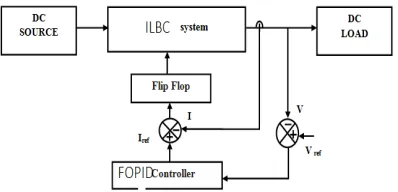
The block diagram of the closed loop ILBC system is appeared in Figure 2.1. A constant DC is changed over to a variable DC utilizing ILBC and its output is connected to the DC stack. The Control circuit creates pulses for the ILBC.
ISSN (Print) : 2320 – 3765 ISSN (Online): 2278 – 8875
I
nternational
J
ournal of
A
dvanced
R
esearch in
E
lectrical,
E
lectronics and
I
nstrumentation
E
ngineering
(A High Impact Factor, Monthly, Peer Reviewed Journal)
Website: www.ijareeie.com
Vol. 7, Issue 3, March 2018
III. ANALYSIS
Equivalent L and C are expressed as follows:
L = ……….. (1)
C = ………. (2)
Output of PI is as follows:
Vo= K1 e + K2 ʃedt + K3 de/dt…. (3)
Efficiency is calculated as follows:
ή=V2I2 / V1I1 ……….. (4)
IV. SIMULATION RESULTS
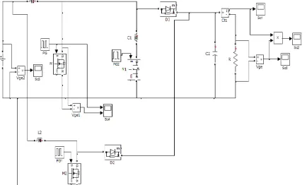
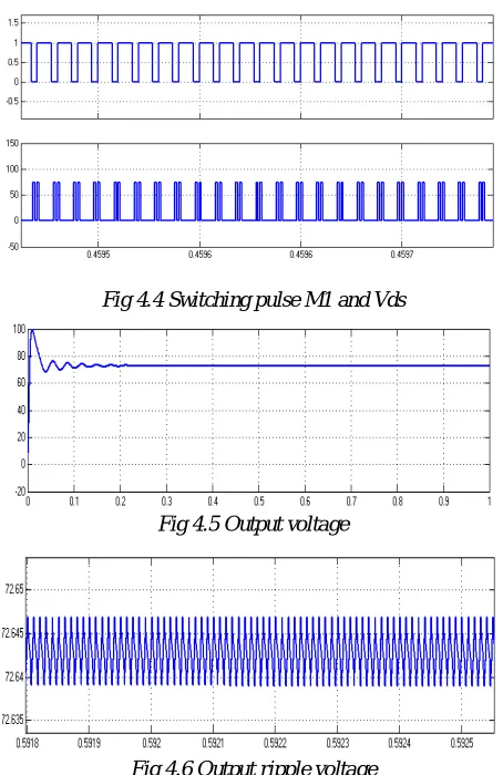
The circuit diagram of the conventional interleaved boost converter is shown in Fig 4.1. The input voltage is shown in Fig 4.2 and its value is 15V. The Switching pulse for the switches M1 and M2 are shown in Fig 4.3 and its peak-to-peak value is 1V. The Switching pulse for the switches M1 and Vds is shown in Fig 4.4. The value of M1 is 1V and the value of Vds is 75V. The output voltage is shown in Fig 4.5 and its value is 75V. The Output ripple voltage is appeared in 4.6 and its value is 72.650V. The Output current is shown in Fig 4.7 and its value is 0.11A. The output power is appeared in Fig 4.8 and its value is 8 watts.
Fig 4.1 Circuit diagram of the conventional interleaved boost converter
ISSN (Print) : 2320 – 3765 ISSN (Online): 2278 – 8875
I
nternational
J
ournal of
A
dvanced
R
esearch in
E
lectrical,
E
lectronics and
I
nstrumentation
E
ngineering
(A High Impact Factor, Monthly, Peer Reviewed Journal)
Website: www.ijareeie.com
Vol. 7, Issue 3, March 2018
Fig 4.3 Switching pulse for M1and M2
Fig 4.4 Switching pulse M1 and Vds
Fig 4.5 Output voltage
ISSN (Print) : 2320 – 3765 ISSN (Online): 2278 – 8875
I
nternational
J
ournal of
A
dvanced
R
esearch in
E
lectrical,
E
lectronics and
I
nstrumentation
E
ngineering
(A High Impact Factor, Monthly, Peer Reviewed Journal)
Website: www.ijareeie.com
Vol. 7, Issue 3, March 2018
Fig 4.7 Output current
Fig 4.8 Output power
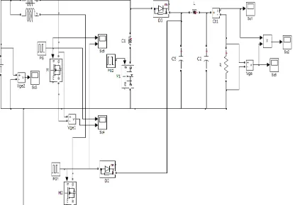
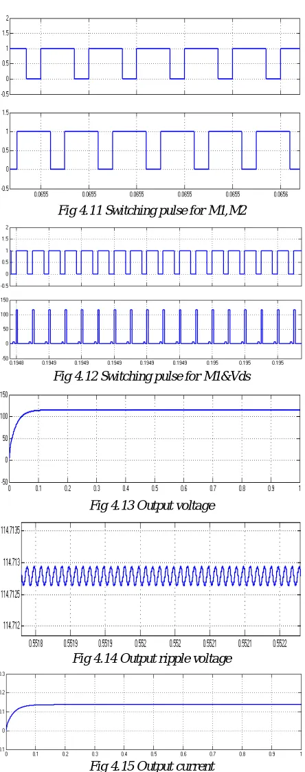
The circuit diagram of the proposed interleaved boost converter is appeared in Fig 4.9. The input voltage is appeared in Fig 4.10 and its value is 15V.The switching pulse for M1, M2 are shown in Fig 4.11 and its peak-to-peak value is 1V. The Switching pulse M1 &Vds is appeared in Fig 4.12. The value of M1 is 1V and the value of Vds is 125V. The output voltage is shown in Fig 4.13 and its value is 120V. The output ripple voltage is appeared in Fig 4.14 and its value is 114.7112V. The output current is shown in Fig 4.15 and its value is 0.13A. The output power is appeared in 4.16 and its value is 17 watts. The comparison of output voltage ripple, output voltage, and output power is given in Table-1.
Fig 4.9 Circuit diagram of the proposed interleaved boost converter
ISSN (Print) : 2320 – 3765 ISSN (Online): 2278 – 8875
I
nternational
J
ournal of
A
dvanced
R
esearch in
E
lectrical,
E
lectronics and
I
nstrumentation
E
ngineering
(A High Impact Factor, Monthly, Peer Reviewed Journal)
Website: www.ijareeie.com
Vol. 7, Issue 3, March 2018
Fig 4.11 Switching pulse for M1,M2
Fig 4.12 Switching pulse for M1&Vds
Fig 4.13 Output voltage
Fig 4.14 Output ripple voltage
ISSN (Print) : 2320 – 3765 ISSN (Online): 2278 – 8875
I
nternational
J
ournal of
A
dvanced
R
esearch in
E
lectrical,
E
lectronics and
I
nstrumentation
E
ngineering
(A High Impact Factor, Monthly, Peer Reviewed Journal)
Website: www.ijareeie.com
Vol. 7, Issue 3, March 2018
Fig 4.16 Output power
Table -1
Comparison of output voltage ripple, output voltage & output power Interleaved
boost converter
Voltage ripple
Vo Po
Conventional 0.01V 72V 9W
Proposed 0.0002V 110V 16W
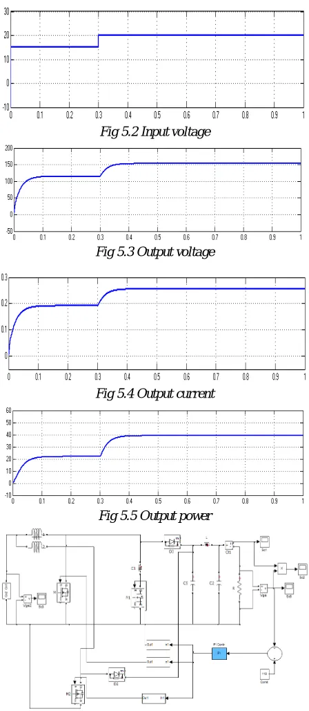
The circuit diagram of the open-loop system with disturbance is appeared in Fig 5.1. The input voltage is appeared in Fig 5.2 and its value is 20 V. The output voltage is appeared in Fig 5.3 and its value is 150V.
Fig 5.1 Circuit diagram of the open loop system with disturbance
ISSN (Print) : 2320 – 3765 ISSN (Online): 2278 – 8875
I
nternational
J
ournal of
A
dvanced
R
esearch in
E
lectrical,
E
lectronics and
I
nstrumentation
E
ngineering
(A High Impact Factor, Monthly, Peer Reviewed Journal)
Website: www.ijareeie.com
Vol. 7, Issue 3, March 2018
Fig 5.2 Input voltage
Fig 5.3 Output voltage
Fig 5.4 Output current
Fig 5.5 Output power
ISSN (Print) : 2320 – 3765 ISSN (Online): 2278 – 8875
I
nternational
J
ournal of
A
dvanced
R
esearch in
E
lectrical,
E
lectronics and
I
nstrumentation
E
ngineering
(A High Impact Factor, Monthly, Peer Reviewed Journal)
Website: www.ijareeie.com
Vol. 7, Issue 3, March 2018
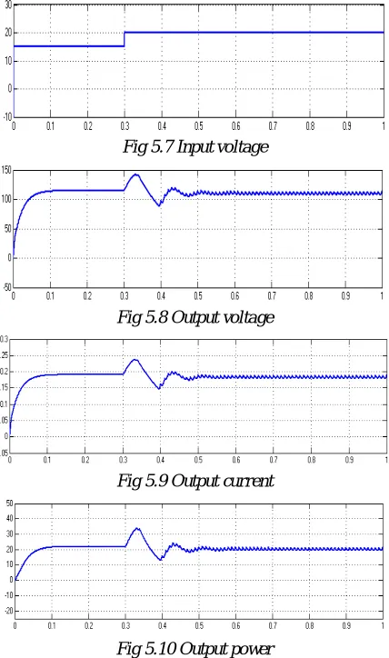
The circuit diagram of the closed loop with PI controller is appeared in Fig 5.6. The input voltage is appeared in Fig 5.7 and its value is 20 V. The output voltage is appeared in Fig 5.8 and its value is 120V. The output current is shown in Fig 5.9 and its value is 0.18A. The output power is appeared in Fig 5.10 and its value is 20 watts.
Fig 5.7 Input voltage
Fig 5.8 Output voltage
Fig 5.9 Output current
Fig 5.10 Output power
ISSN (Print) : 2320 – 3765 ISSN (Online): 2278 – 8875
I
nternational
J
ournal of
A
dvanced
R
esearch in
E
lectrical,
E
lectronics and
I
nstrumentation
E
ngineering
(A High Impact Factor, Monthly, Peer Reviewed Journal)
Website: www.ijareeie.com
Vol. 7, Issue 3, March 2018
Fig 5.11 Circuit diagram of the closed loop system with FOPID controller
The output voltage is appeared in Fig 5.13 and its value is 120V. The output current is shown in Fig 5.14 and its value is 0.19A. The output power is appeared in Fig 5.15 and its value is 20 watts. The comparison of time domain parameters is given in Table-2.
Fig 5.12 Input voltage
Fig 5.13 Output voltage
Fig 5.14 Output current
ISSN (Print) : 2320 – 3765 ISSN (Online): 2278 – 8875
I
nternational
J
ournal of
A
dvanced
R
esearch in
E
lectrical,
E
lectronics and
I
nstrumentation
E
ngineering
(A High Impact Factor, Monthly, Peer Reviewed Journal)
Website: www.ijareeie.com
Vol. 7, Issue 3, March 2018
Table -2
Comparison of Time domain Parameters Controller Rise
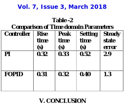
time (s) Peak time (s) Setting time (s) Steady state error PI 0.32 0.33 0.52 2.9
FOPID 0.31 0.32 0.40 1.3
V. CONCLUSION
The PV fed ILBC system is successfully modeled and simulated and the case studies with PI and FOPID controllers are exhibited in detail. It is noticed that the settling time is reduced from 0.3 to 0.23 seconds and the steady-state error in the output power is reduced from 2.8 to 1.9W by replacing the PI controller with the FOPID controller. The results indicate that the FOPID based ILBC gives the best dynamic response. The hardware results are similar to the simulation results for the ILBC system.
The studies indicated that the ILBC system is a viable alternative to the existing converters. The advantages of the suggested system are high voltage gain and reduced steady-state error. The disadvantage of the recommended system is that it is suitable for low power loads only.
The scope of the present work is to compare PI and FOPID based ILBC systems. The comparison with multi-loop control systems will be done in the future.
REFERENCES
[1] IEEE TRANSACTIONS ON POWER ELECTRONICS, VOL. 26, NO. 4, APRIL 2011 1127 ”A Novel High Step-Up DC-DC Converter for a Microgrid System” Yi-Ping Hsieh, Jiann-Fuh Chen, Member, IEEE, Tsorng-Juu Liang, Member, IEEE, and Lung-Sheng Yang
[2] IEEE TRANSACTIONS ON POWER ELECTRONICS, VOL. 29, NO. 7, JULY 2014 3591 “Isolated High Step-Up DC-DC Converter With Low Voltage Stress” FatihEvran and Mehmet TimurAydemir, Member, IEEE
[3] C. Zhang, S. Du, and Q. Chen, “A novel scheme suitable for high-voltage and large-capacity photovoltaic power stations,” IEEE Trans. Ind. Electron., vol. 60, no. 9, pp. 3775–3783, Sep. 2013.
[4] IEEE TRANSACTIONS ON CIRCUITS AND SYSTEMS—I: REGULAR PAPERS, VOL. 55, NO. 4, MAY 2008 1159 “A Family of Single-Switch PWM Converters With High Step-Up Conversion Ratio” Esam H. Ismail, Senior Member, IEEE, Mustafa A. Al-Saffar, Member, IEEE, Ahmad J. Sabzali, Member, IEEE, and Abbas A. Fardoun, Senior Member, IEEE
[5] IEEE TRANSACTIONS ON POWER ELECTRONICS, VOL. 30, NO. 2, FEBRUARY 2015 “High Step-Up Converter with Three-Winding Coupled Inductor for Fuel Cell Energy Source Applications” Kuo-Ching Tseng, Jang-Ting Lin, and Chi-Chih Huang
[6] IEEE JOURNAL OF EMERGING AND SELECTED TOPICS IN POWER ELECTRONICS, VOL. 04, NO. 2, JUNE 2016 363 “A Single-Switch Converter With High Step-Up Gain and Low Diode Voltage Stress Suitable for Green Power-Source Conversion” Kuo-Ching Tseng, Chi-Chih Huang, and Chun-An Cheng, Member, IEEE
[7] High Step-Up Trans-Inverse (Tx-1) DC-DC Converter for Distributed Generation System Yam P. Siwakoti, Member, IEEE, FredeBlaabjerg, Fellow, IEEE, Poh Chiang Loh search ---2015 publishing details
[8] IEEE TRANSACTIONS ON INDUSTRIAL ELECTRONICS, VOL. 57, NO. 6, JUNE 2010 “A High-Efficiency High Step-Up Converter WithLow Switch Voltage Stress for Fuel-CellSystem Applications” Ching-Tsai Pan, Member, IEEE, and Ching-Ming Lai, Student Member, IEE [9] “Novel Isolated High-step-up DC-DC Converter with Voltage” LiftTsorng-Juu Liang, Member, IEEE, Jian-Hsieng Lee, Shih-Ming Chen, Jiann-Fuh Chen, Member, IEEE, and Lung-Sheng Yang 2011 --- search publication
[10]. IEEE TRANSACTIONS ON POWER ELECTRONICS, VOL. 30, NO. 8, AUGUST 2015 4255 “A Novel High Step-up DC/DC Converter Based on Integrating Coupled Inductor and Switched-Capacitor Techniques for Renewable Energy Applications” Ali Ajami, HosseinArdi, and Amir Farakhor
[11] IEEE TRANSACTIONS ON INDUSTRIAL ELECTRONICS, VOL. 58, NO. 4, APRIL 2011 1239 “Review of Non-isolated High-Step-Up DC/DC Converters in Photovoltaic Grid-Connected Applications” Wuhua Li, Member, IEEE, and Xiangning He, Fellow, IEEE
[12.] IEEE TRANSACTIONS ON POWER ELECTRONICS, VOL. 28, NO. 1, JANUARY 2013 “Interleaved High Step-Up ZVT Converter With Built-In Transformer Voltage Doubler Cell for Distributed PV Generation System” Weichen Li, Xin Xiang, Chushan Li,