SUBSTRATE INTEGRATION OF DUAL INDUCTIVE POST WAVEGUIDE FILTER
A. Adabi and M. Tayarani
Electrical Engineering Department IUST University
Narmak, Tehran, Iran
Abstract—Integration of planar circuits to non-planar ones has been recently considered as a credible technique for low-cost mass production of microwave and millimeter-wave circuits andsystems. This paper regards these concepts that provide for a complete integration of planar circuits andwaveguide filters synthesizedon a single substrate by means of metalizedpost (via-hole) arrays. A methodof designing a waveguide filter derived from a synthesis technique using dual array of inductive posts is presented. An experimental five-pole Chebyshev filter which has 2.5 dB insertion loss and return loss better than 10 dB is demonstrated. Such a technique of integration of planar andnon-planar circuits on the same substrate shows a significant reduction in size, weight and cost.
1. INTRODUCTION
Rectangular waveguide has been one of the best candidates to design a high-Q component in microwave and millimeter-wave systems during decades. One of the difficulties that engineers will encounter in integrating such a component with planar circuits is the requirement of a 3-D complex transition. Several studies of transitions between microstrip line andrectangular waveguide have been reported [13– 16, 24, 25]. However, typical integration designs from rectangular waveguide filters with planar structures are voluminous and expensive to manufacture, due to the fact that rectangular waveguide components intrinsically are bulky andcostly. Moreover, high precision mechanical adjustment or a subtle tuning mechanism is needed to obtain satisfying performance of filters for mass production.
advantages of printed circuits such as low cost, small size etc. and has the benefits of being waveguide such as high quality factor (Q-factor), low insertion loss, etc. The SIW is synthesizedandrealizedwith two arrays of metalizedposts or via-holes on two sides of the PCB that is simulating the side walls of the standard rectangular waveguide. Due to the fact that two metal planes cover the up anddown surfaces of the SIW components, there will be no anxiety of outside interference that may come from the planar circuit is integrating with SIW. The rapiddevelopment andgreat influence of SIW technique in designing of many passive components andactive devices such as antennas [7], filters [8], diplexers [9], oscillators [10], and couplers [11] indicates the promising capabilities of this technology for designing microwave and millimeter-wave devices and systems. In this paper a dual inductive post waveguide filter design process and fabrication data at X-band are presented. Initially, we begin with a brief analysis of integrated-waveguide in Section 2 and continue in Section 3 by presenting the design process of (dual) inductive post waveguide filters and the finally the physical parameters for implementing the filter on PCB are tabled. Also, the simulation andmeasurement results are includedin Section 4.
2. ANALYSIS OF INTEGRATED WAVEGUIDE
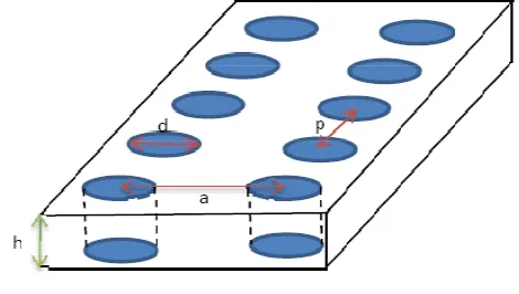
Figure 1 shows the schematic view of the integratedwaveguide. This waveguide consists of two parallel arrays of metalized posts (or via-holes) that resemble the side walls of a real standard waveguide. Generally, a rectangular waveguide has horizontal length,aandvertical length, b andits cut-off frequencies dependon a and b as (1),
which, µ and ε are permeability andpermittivity of the substrate, respectively [15].
fCmn = KC 2π√µ=
1 2π√µ×
(mπ/a)2+ (nπ/b)2 →f
C10=
1 2aõ
(1)
Since the height of substrate in SIW is the same as vertical wall andas long as the substrate thickness (h orb) is much smaller thana, the cut-off frequency of the dominant mode in rectangular waveguide (TE10) is determined only bya.
According to the analysis reported in [2], to realize the minimum radiation loss as well as the return loss, the parameters of via-holes “d” and“p” shouldbe kept as dp ≥0.5 and da <0.4. Also, the distance between via-holes (p) has to be smaller than 0.2λ.
3. DUAL INDUCTIVE POST-FILTER DESIGN
Bandpass waveguide filters can be realized with different structures like
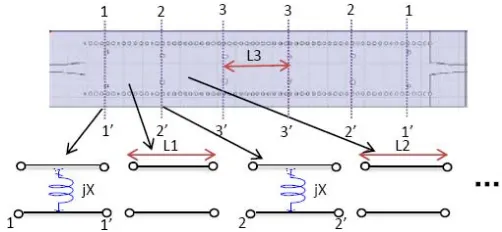
E-plane or H-plane, irises, and metalized cylindrical inductive posts [16–21]. Metalized cylindrical inductive post filter surpasses the other techniques for ease of implementation in SIW technology. Marcuwitz proposed two methods for designing single inductive post filters as Off-Centeredpost andCenteredpost filters [5]. The former usually result in vias of same diameter while the latter gives vias of different diameters. Two symmetrically placed posts have some advantages over a single post. Intuitively, the extent of the higher-order fields might be expectedto be smaller in the symmetrical case for the same given susceptance. This is due to the fact that no second-order mode is excitedin this case. It is thus possible to put the matching structure closer to the loadimpedance without affecting its susceptance [1]. The geometry of the problem is shown in Fig. 2.
As illustratedin Fig. 2(b) the susceptance is to be foundfor the dominant mode (TE10) with electric vector parallel to the posts. By assuming that the current in the post is uniform andthat for the purpose of calculating the fields excited in the guide, the currents are concentratedalong the axis of each post, Gruenberg developedsome formulas for calculating the susceptance [1]. Also, it has been shown that the equivalent network is then transformedinto aK-inverter using (2) [6].
K =Z0tan|φ/2|
φ=−tan−1 2X
Z0
(a) (b)
(c)
Figure 2. Dual inductive post filters design process. (a) Posts in waveguide. (b) Equivalent lumped circuit (c) Equivalent K-inverter network.
Figure 3. Equivalent circuit of waveguide filter.
In Fig. 3, the equivalent circuit of the whole filter is shown. It is clear that the cavity between the posts behaves as a half-wavelength resonator andthe posts play their the role of theK-inverter.
waveguide, as depicted in [6]. Usually, inductive post filters that use a number of posts of different diameter located at the same distance from the side walls will result in some unfeasible via-holes on the PCB process. So, to resolve the problem, we considered both the distance from sidewalls and the diameter of the posts as variable parameters. The geometry of the filter is shown in Fig. 3.
4. EXPERIMENTAL RESULTS
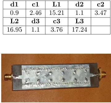
Following the rule presentedin Section 3, a five-pole Chebyshev filter of 500 MHz bandwidth centred at 8.2 GHz has been designed, fabricated andmeasured. We useda 0.7874 mm-thick dielectric substrate with
r = 2.6 andtanδ = 0.0006 (Taconic, TLT) to construct the circuit. The dimensions of the structure according to Fig. 1 are selected as,
a = 14.9 mm, p = 1.5 mm, h = 0.7874 mm andthe post diameter
d = 0.8 mm. A well-known taperedmicrostrip transition has been designed and employed as described perfectly in [4]. The dimensions of the transition regarding Fig. 1 of [4] are,w= 2.2 mm,d= 3.8 mm, and
l = 6.5 mm. Also the dimensions of the filter’s posts are summarized in Table 1.
Table 1. Dimensions of the deigned filter. All the dimensions are in mm.
d1 c1 L1 d2 c2
0.9 2.46 15.21 1.1 3.47
L2 d3 c3 L3
16.95 1.1 3.76 17.24
Figure 4. Photograph of the manufacturedfive-pole Chebyshev filter.
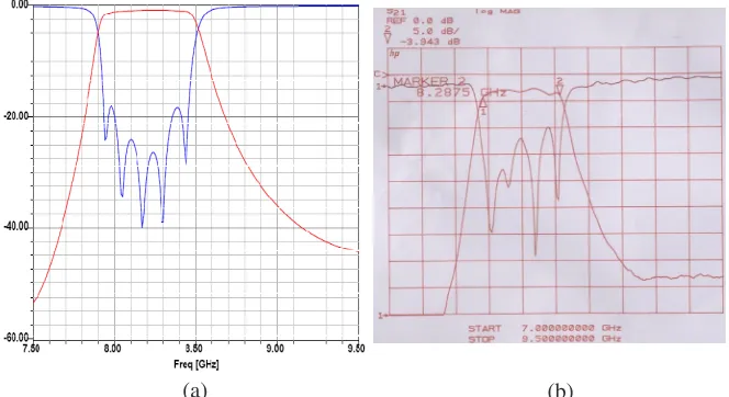
around2.5 dB andthe return loss is better than 10 dB in the pass band. The insertion loss discrepancy between the simulated result andthe measuredone is because of that the commercial package used for simulation is not accurate for small thickness conductors, so the conductor losses were not modelled in the simulation. Also, the best manufacturing precision that we couldapply is 100 microns andas it can be seen in Fig. 4 we filledall the via-holes since we were not sure that the posts have been metalizedcompletely, so a sensible discrepancy was expected.
(a) (b)
Figure 5. (a) Simulatedand(b) measuredresults for five-pole Chebyshev filter with two transitions of microstrip to integrated waveguide.
5. CONCLUSION
REFERENCES
1. Gruenberg, H., “Symmetrical placedinductive posts in rectangu-lar wave guide,” Radio and Electrical Engineering Division, Na-tional Research of Canada, Ottawa, Canada, December 1951. 2. Deslandes, D. and K. Wu, “Single-substrate integration technique
of planar circuits and waveguide filters,” IEEE Transactions on Microwave Theory and Techniques, Vol. 51, No. 2, February 2003. 3. Kim, B. S., J. W. Lee, K. S. Kim, andM. S. Song, “PCB substrate integratedwaveguide-filter using via fences at millimeter-wave,”
IEEE MTT-S Digest, 2004.
4. Deslandes, D. andK. Wu, “Integratedmicrostrip andrectangular waveguide in planar form,” IEEE Microwave and Wireless Components Letters, Vol. 11, No. 2, February 2001.
5. Marcuvitz, N.,Waveguide Handbook, Peter Peregninus Ltd., 1985. 6. Matthaei, G. L., et al., Microwave Filters, Impedance Matching
and Coupling Structures, Artech House, 1980.
7. Sanz Izquierdo, B., P. R. Young, N. Grigoropoulos, J. C. Batche-lor, andR. J. Langley, “Substrate-integratedfoldedwaveguide slot antenna,”IEEE International Workshop on Antenna Technology: Small Antennas and Novel Metamaterials, 2005.
8. Chen, X., W. Hong, T. Cui, J. Chen, andK. Wu, “Substrate integrated waveguide (SIW) linear phase filter,”IEEE Microwave and Wireless Components Letters, Vol. 15, No. 11, November 2005. 9. Hao, Z. C., W. Hong, J. X. Chen, X. P. Chen, andK. Wu, “Planar diplexer for microwave integratedcircuits,” IEE Proc.-Microw. Antennas Propag., Vol. 152, No. 6, December 2005.
10. Cassivi, Y. andK. Wu, “Low cost microwave oscillator using substrate integrated waveguide cavity,” IEEE Microwave and Wireless Components Letters, Vol. 13, No. 2, February 2003. 11. Hao, Z. C., W. Hong, J. X. Chen, H. X. Zhou, andK. Wu, “Single
layer substrate integrated waveguide directional couplers,” IEE Proc. - Microw. Antennas Propag., Vol. 153, No. 5, October 2006. 12. Deslandes, D. andK. Wu, “Integratedmicrostrip andrectangular waveguide in planar form,” IEEE Microwave Wireless Comp. Lett., Vol. 11, 68–70, February 2001.
13. Deslandes, D. andK. Wu, “Integratedtransition of coplanar to rectangular waveguides,” IEEE MTT-S Int. Microwave Symp. Dig., Vol. 2, 619–622, 2001.
Int. Microwave Symp. Dig., Vol. 2, 623–626, 2001.
15. Nam, H., T.-S. Yun, K.-B. Kim, K.-C. Yoon, andJ.-C. Lee, “Ku-bandtransition between microstrip andsubstrate integrated waveguide (SIW),” IEEE APMC 2005 Proceedings, 2005.
16. Sotoodeh, Z., F. H. Kashani, and H. Ameri, “A novel bandpass waveguide filter structure on SIW technology,” Progress In Electromagnetics Research Letters, Vol. 2, 141–148, 2008.
17. Ghorbaninejad, H. and M. Khalaj-Amirhosseini, “Compact bandpass filters utilizing dielectric filled waveguides,”Progress In Electromagnetics Research B, Vol. 7, 105–115, 2008.
18. Deslandes, D. and K. Wu, “Millimeter-wave substrate integrated waveguide filters,”IEEE CCECE2003, 1917–1920, 2003.
19. Bahrami, H., M. Hakkak, andA. Pirhadi, “Analysis anddesign of highly compact bandpass waveguide filter using complementary split ring resonators (CSRR),” Progress In Electromagnetics Research, PIER 80, 107–122, 2008.
20. Khalaj-Amirhosseini, M., “Microwave filters using waveguides filledby multi-layer dielectric,” Progress In Electromagnetics Research, PIER 66, 105–110, 2006.
21. Mohammad Amjadi, S. and M. Soleimani, “Design of bandpass waveguide filter using frequency selective surfaces loaded with surface mount capacitors basedon split-fieldupdate FDTD method,” Progress In Electromagnetics Research B, Vol. 3, 271– 281, 2008.
22. Zhang, X.-C., Z.-Y. Yu, andJ. Xu, “Novel band-pass substrate integrated waveguide (SIW) filter based on complementary split ring resonators (CSRRs),”Progress In Electromagnetics Research, PIER 72, 39–46, 2007.
23. Li, G. andC.-H. Liang, “Design techniques for microwave diplexers,”Progress In Electromagnetics Research B, Vol. 2, 103– 113, 2008.
24. Lee, Y., “CPW-to-stripline vertical via transitions for 60 GHz LTCC SOP applications,” Progress In Electromagnetics Research Letters, Vol. 2, 37–44, 2008.
25. Eldek, A. A., “Wideband 180 degree phase shifter using microstrip-CPW-microstrip transition,” Progress In Electromag-netics Research B, Vol. 2, 177–187, 2008.
26. Ranjkesh, N. andM. Shahabadi, “Loss mechanisms in SIW and MSIW,” Progress In Electromagnetics Research B, Vol. 4, 299– 309, 2008.
“Investigation on the ohmic conductor losses in substrate-integrated waveguide and equivalent rectangular waveguide,” J. of Electromagn. Waves and Appl., Vol. 21, No. 6, 769–780, 2007. 28. Zhu, Y.-Z. andY.-J. Xie, “Novel microstrip bandpass filters
with transmission zeros,”Progress In Electromagnetics Research, PIER 77, 29–41, 2007.
29. Prabhu, S., J. Mandeep, and S. Jovanovic, “Microstrip bandpass filter at S bandusing capacitive coupledresonator,” Progress In Electromagnetics Research, PIER 76, 223–228, 2007.
30. Zhao, L.-P., X. Zhai, B. Wu, T. Su, W. Xue, andC.-H. Liang, “Novel design of dual-mode bandpass filter using rectangle structure,”Progress In Electromagnetics Research B, Vol. 3, 131– 141, 2008.
31. Wang, Y.-X., B.-Z. Wang, andJ. P. Wang, “A compact square loop dual-mode bandpass filter with wide stop-band,”Progress In Electromagnetics Research, PIER 77, 67–73, 2007.
32. Chen, J., Z.-B. Weng, Y.-C. Jiao, andF.-S. Zhang, “Lowpass filter design of Hilbert curve ring defected ground structure,”Progress In Electromagnetics Research, PIER 70, 269–280, 2007.
33. Hasan, A. andA. E. Nadeem, “Novel microstrip hairpinline narrowbandbandpass filter using via groundholes,” Progress In Electromagnetics Research, PIER 78, 393–419, 2008.
34. Wu, G.-L., W. Mu, X.-W. Dai, andY.-C. Jiao, “Design of novel dual-band bandpass filter with microstrip meander loop resonator andCSRR DGS,” Progress In Electromagnetics Research, PIER 78, 17–24, 2008.