ABSTRACT
Varma, Ambrish Kant. Computer - Aided Tools for Seamless High Density
Interconnects. (Under the direction of Paul D. Franzon)
This thesis presents the tool-set designed to demonstrate the possibility of using the
Cadence tools to design, verify and extract circuitry on the substrate along with the
on-chip design. This circuitry could be an inter-chip connection that connects two
different chips or an intra-chip connection where a long interconnect is taken off from
the active area of the chip to the substrate and back on to the same chip.
To be able to do this task, the work for this project is broadly classified into four
different categories. These are writing
•
The technology file and the display.drf file
•
The Design Rule Check deck
•
The Layout Verses Schematic deck
•
The Extraction deck
After having completed the above-mentioned tasks, the tool-set was also tested and
COMPUTER – AIDED TOOLS
FOR
SEAMLESS HIGH DENSITY INTERCONNECTS
by
AMBRISH KANT VARMA
A thesis submitted to the Graduate Faculty
of
North Carolina State University
In partial fulfillment of the requirement for the Degree in
Master of Science in Computer Engineering
Department of Electrical and Computer Engineering
Raleigh
2001
Approved by:
_____________________
Dr. Paul D Franzon
Chairman, Advisory Committee
_________________
___________________
BIOGRAPHY
Ambrish Kant Varma was born in Allahabad, India in the year 1974. He attended his
high school at Allahabad and went on to attend the University of Allahabad pursuing
the Bachelors of Science program in Statistics. After completing one year in this
university, he had the opportunity to go to Sydney, Australia to complete his
undergraduate studies in Electrical Engineering. After graduating with honors from
the University of Western Sydney, Nepean in 1999, Ambrish decided to take his
academic qualification a step further and was admitted to the University of Louisiana
at Lafayette in the fall of 1999. He decided to take a transfer to North Carolina State
University in spring 2000 where he began work under the guidance of Dr. Paul. D.
Franzon. He worked as an intern at the IBM facility at Research Triangle Park, North
ACKNOWLEDGEMENTS
There is never a job in the world that can be done single handedly. This work was no
exception. Let me begin by naming my advisor, Dr. Paul D Franzon, who was always
available for any doubt or question, howsoever elementary or trivial they might be.
Without his insight and guidance, needless to say, this project would have never got
completed. Also, many thanks to my committee members, Dr. Byrd and Dr.
Rotenberg, for their valuable input, encouragement and for reviewing my thesis.
Special thanks to Alan Glaser, who, in spite of being extremely busy with his own
research and thesis work, never got irritated with all the terribly silly questions that I
hurled at him. There was not one email he didn’t reply to and there was not one
question he didn’t have an answer for. Thank you Alan for all you’ve done.
Thanks also to Stephen Mick, John Damiano, Pronita Mehrotra and Nishith Rohatgi
for helping me out whenever I got stuck. Whether it was using Cadence,
programming in Skill or simple printer problems, I didn’t have to look far for help.
Needless to say, they deserve accolades as much as I do.
Guorong Ma helped me in this project as though his life depended on it. Your
sincerity, dedication and hard work were a source of inspiration to me. Thank you for
your late nights and for tolerating me.
Thanks to the Department of Electrical and Computer Engineering for EGRC 438. It
will always have a special place in my heart and indeed, it will be a sacred place to
me for the rest of my life. Thanks also to Michelle Joyner, who never let me worry
about anything except my research. Thanks Michelle.
Thanks also to my EGRC 438 labmates for creating such an exciting and relaxed
environment to work in. Good luck in your endeavors.
Lastly, my sincerest thanks to my family, who even though far away, never lost hope
TABLE OF CONTENTS
List of Tables ... vi
List of Figures... vii
1
I
NTRODUCTION ANDO
VERVIEW... 1
1.1 Research objectives and Approach ... 3
2
B
ACKGROUND ANDL
ITERATUREREVIEW ... 5
2.1 SHOCC and MCM ... 6
2.2 Past Work ... 8
2.2.1
The NCSU Cadence Design Kit (NCSU CDK) ...8
3
T
HET
ECHNOLOGYF
ILE... 10
3.1 Features... 11
3.2 To Add a Layer ... 13
3.3 The Display Resource file (display.drf) ... 15
4
T
HED
IVAD
ECK... 16
4.1 Design Rule Check... 16
4.1.1
Key Features of the DRC rule File ...17
4.1.1.1 Separation Between Same Metal Layer ...17
4.1.1.2 Separation Between Two Different Layers ...17
4.1.1.3 Metal - Via Enclosure ...18
4.1.2
Design Rule Check – A Demonstration...19
4.1.3
MCM DRC Rule list...23
4.2 Extraction... 25
4.2.1
Why Transmission Lines?...25
4.2.2
Key Features of the Extraction File...26
4.2.2.1 The Solder Bump...26
4.2.2.2 The Y model of the U element ...26
4.2.2.3 The X model of the U element ...27
4.2.2.4 Connecting the Pieces ...27
4.2.2.5 Calculate Lengths of Transmission Line ...28
4.2.3
How Models Are Linked ...28
4.3 Layout Vs Schematic... 30
4.3.1.1 permuteDevice...30
4.3.1.2 compareDeviceProperty ...31
4.3.1.3 removeDevice...31
4.3.1.4 ignoreTerminal ...31
4.3.1.5 Series and Parallel Reduction ...31
4.3.1.6 MOS Reduction ...32
4.3.2
The Error Files ...32
5
C
ASES
TUDY– D
RIVERR
ECEIVERC
IRCUIT... 35
5.1 Layout and DRC ... 36
5.2 Extraction... 38
5.3 LVS ... 40
5.4 Netlist Generation ... 40
5.5 Simulation... 43
6
C
ONCLUSION ANDF
UTUREW
ORK... 44
References ... 48
Appendix A – The Technology File ... 51
Appendix B - display.drf file ... 67
Appendix C - divaDRC.rul file... 68
Appendix D - D Extraction Rule File ... 73
Appendix E - Layer Definition file ... 83
Appendix F – The HSPICE Netlist ... 95
Appendix G – Transmission Line Models ... 97
UMODEL X...97
UMODEL Y...97
BUMP...97
List of Tables
T
ABLE1: N
EWL
AYERS FORSHOCC ...11
List of Figures
F
IGURE1: T
HESHOCC S
TRUCTURE...5
F
IGURE2: A H
IGH PERFORMANCESHOCC IC (
REFERENCE[7])...7
F
IGURE3: LSW
WINDOW...12
F
IGURE4: T
HES
UBSTRATEL
AYERS
TRUCTURE(
CROSS SECTION VIEW)...14
F
IGURE5: T
HES
UBSTRATEL
AYERS
TRUCTURE(T
OP VIEW)...14
F
IGURE6: DRC S
EPARATION(
SAME LAYER) ...17
F
IGURE7: DRC S
EPARATION(
DIFFERENT LAYERS)...17
F
IGURE8: DRC E
NCLOSURE COMMAND...18
F
IGURE9:
FIGURE WITHDRC
ERROR...19
F
IGURE10:
FIGURE WITH ERROR REMOVED...19
F
IGURE11:
FIGURE WITH ERROR...21
F
IGURE12:
FIGURE WITH ERROR REMOVED...21
F
IGURE13: T
HESCHOCC P
ARADIGM...25
F
IGURE14 E
XTRACTEDBUMP S
YMBOL...26
F
IGURE15 E
XTRACTEDUM
ODEL...27
F
IGURE16 T
HEB
UMPS
UBCIRCUIT...29
F
IGURE17: D
RIVER ANDR
ECEIVER CIRCUIT...35
F
IGURE18: T
HED
RIVER- I
NVERTERL
AYOUT...36
F
IGURE19: T
HEE
XTRACTEDC
IRCIUT...39
F
IGURE20: S
CHEMATIC OF THED
RIVER- I
NVERTER CIRCUIT...40
1 INTRODUCTION
AND
OVERVIEW
“Seamless High Off-Chip connectivity (SHOCC) is a combined packaging,
interconnect, and IC design philosophy and associated enabling technology that aims
to shift the device fabrication paradigm from today’s single die approach to a parallel
manufacturing scheme that utilizes yield-optimized IC elements packaged using a
high-performance interconnect element” [1]. The main idea behind the concept is that
the interconnects on the chip in a one die system are divided between on-chip and
off-chip interconnects. This eliminates the possibility of having long lossy
transmission lines on the chip. Consider that interconnects on the chip are aluminum
which has a high resistance (
ρ
= 4.5
µΩ
-cm). Interconnects off the chip can be
fabricated using copper that has low resistance (
ρ
= 1.67
µΩ
-cm), hence reducing the
RC losses as per the equation below).
Also, as designers are hard pressed to reduce the size of the chip, the area of the
interconnects on the chips are bound to decrease, resulting in an increase in the
improvement that can be achieved is smaller chip size as a lot of area occupying
interconnects is now brought off the chip on the substrate.
Also the number of inputs/outputs that the chip can handle can improve drastically
considering that I/O can be done using the solder-pads on the chip that are distributed
all over the area of the chip (in a multi-chip module) as compared to a single die
where all the inputs/outputs have to be brought out to the perimeter of the chip.
The SHOCC interconnects are modeled as lossy transmission line elements. This is
done so that the designer can obtain accurate chip-chip delay and cross-talk noise
estimates when evaluating the performance of the chip. This gains importance when
the rise time of the signals reduces as compared to the flight time of the signal through
the chip.
This project is meant to put into practice the idea of SHOCC and to test it using a
practical circuit. This thesis aims at documenting the work done in writing the
technology files that support the extension of the traditional layout methodology to
the level of SHOCC and the rules file that have to be written in order to test and
extract the design. Chapter 3 covers the technology file and the display resource file
that describes the layers physical appearance. The technology file permits
independent or co-layout of the chip, substrate and solder bumps in the Cadence
Virtuoso layout package.
Chapter 4 covers the Diva Deck – a set of rule files that allow complete design rule
check, extraction of the design and a Layout versus Schematic test that checks the
correctness of the extracted design against a schematic provided by the user. The
extraction deck permits co-extraction of the IC and the SHOCC interposer, producing
a HSPICE file in which on chip circuits are represented by transistors and parasitic
capacitance and off chip SHOCC lines are captured as U element transmission lines
Chapter 5 discusses the circuit that has been used to test the technology file and the
rules file have been put to test. This chapter also contains the netlist that is generated
and the result of the simulations.
Chapter 6 discusses the future work that can be added on to the current work and also
serves as a conclusion to this thesis.
The thesis is written in a manner in which a complete newcomer in this field would be
able refer to it as a guide to grasp the subject matter and, if required, add to or modify
the current work. Each section is accompanied by an extensive explanation of the
SKILL and DIVA functions that have been used as well as illustrated with examples.
A webpage has also been designed that includes user manuals, installation
instructions, and all the scripts corresponding to this project. The URL of the website
is:
http://www.ece.ncsu.edu/cadence/SHOCC_Kit/SHOCC_home.html
1.1
RESEARCH OBJECTIVES AND APPROACH
The main objective of this research is to develop a CAD tool set useful for the
co-design and analysis of chips and substrate employing the SHOCC paradigm. The
traditional chip design process involves design capture, checking the geometric
viability of the design, and extraction of the design to a form that can be understood
by a fabrication house such as MOSIS
1. The intention with this project was to have a
kit within the Cadence environment that could do all of the above as well as have the
capability of utilizing the substrate layers for the placement of long interconnects for
intra-chip connections as well as interconnects for inter-chip connections. The
designer can choose to only look at the IC design, I/O pad design or substrate design
as he pleases. Also the design can be interactively modified as seen fit. As mentioned
before, a design rule checker can be invoked to check if the design is fit to be
manufactured and all rules are being obeyed. Along with the design rule checking, our
objective was also to write a Layout versus Schematic procedure so that a designer
1
will be able to check that the final layout is equivalent connection-wise to a supplied
schematic.
The design kit was to be developed within the Cadence IC environment to permit
co-design and analysis of SHOCC co-designed chips and substrates. The new technology
files and the rules files would be developed by using the SKILL programming
language within the Cadence environment, as would be the extraction process that
would permit the co-extraction of the on-chip parasitics into a high fidelity HSPICE
file.
Performance verification will be conducted by modifying the extraction routines so
that the SHOCC interconnects are extracted as transmission lines and are represented
as U models in an appropriate HSPICE file.
A few other objectives were decided upon before the start of the project, but these
were subject to the availability of time and resources. One of them was to investigate
the possibility of having a Post Extraction Filter. This filter would allow us to extract
only a certain net or a specific area of the circuit instead of extracting the entire
circuit. Another capability that the tool-set could have was the auto-routing feature.
Currently connections on the on-chip circuit that are on the same electrical net can be
auto-routed. A similar feature can be extended to the on-chip and the off-chip
2 BACKGROUND AND LITERATURE REVIEW
A substantial amount of research has been done in the area of off chip connectivity.
Authors have talked in detail about the advent, need, and advantages of this
technology [1], [6] and [7] and have gone as far as specifying the implementation of
the computer-aided design (CAD) tools that support the SHOCC methodology as one
of the long-term objectives of their project [6].
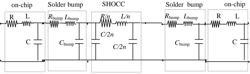
An interesting comparison is made between the performance of SHOCC interconnects
with that of typical on-chip interconnects [7]. Figure 1 shows the various elements of
the transmission line model of the SHOCC paradigm.
Figure 1: The SHOCC Structure
R
bumpL
bumpR
L
C
on-chip
Solder bump
C
bumpR/n
L/n
C/2n
C/2n
SHOCC
Solder bump
R
bumpL
bumpC
bumpR
L
It clearly shows the way the on-chip and the off-chip circuit elements are modeled.
The on-chip elements are represented as lumped L models whereas the off-chip circuit
for the SHOCC line is represented by subdividing the line into 16 subsections. Shown
in the figure is a
π
model of one of the subsections.
The authors modeled a driver – receiver circuit using Maxwell tools and extracted R,
L and C for the SHOCC and its related structures. Simulation of the circuits was done
using Maxwell Spice and PSPICE. Using the R, L and C values, transmission line
spice model for the SHOCC structure was prepared. The authors draw several
conclusions. An interesting results is that the rise time of the output waveform for
on-chip lines is severely degraded as the line length is increased whereas for the SHOCC
line there is no degradation. Also the delay in a SHOCC line increases linearly with
length, whereas it varies exponentially for the on-chip line. A lot of mathematical
results that the authors have derived using simulations in this paper have been used in
this research work.
2.1
SHOCC AND MCM
MCMs can be said to be the originator of the idea of SHOCC. Authors talk about how
performance and cost advantage can be gained if a chip-set is optimally redesigned to
take advantage of the high wire density, fast interconnect details, and high pin counts
available in MCM-D / flip-chip technology [6]. However, the authors say there are
very few commercial digital system design that have migrated to this technology. The
reason is that current design methods optimize chips for single chip packaging –
hence the designers under-utilize the potential of MCM-D / flip-chip technology.
This project is a step forward in removing this drawback. We have demonstrated that
multi-chip packaging is possible with wider and better substrate interconnects that can
be made of copper (
ρ
= 1.67
µΩ
-cm) instead of aluminum/copper (
ρ
= 4.05
µΩ
-cm).
The paper talks about partitioning a large, low-yielding chip to a set of smaller
high-yielding chips. Even though the idea of SHOCC was not developed during those days,
the authors, nevertheless, were moving in that direction.
Several advantages and other issues are discussed regarding the paradigm shift
packaging. Of particular interest is the reduction in delay between on-chip
interconnects and off-chip interconnects. Also, the global power and ground
distribution could be moved off–chip, thus saving valuable on chip resources and real
estate. Also, the MCM inter-chip interconnects can be built using substantially
smaller drivers than those used traditionally for inter-chip signaling.
Even though SHOCC and MCM are fundamentally similar, there are some key
differences between these two technologies [1]. The most notable difference is that
MCM can be made with traditionally designed chips whereas the SHOCC technology
can be implemented using only specifically designed chips. This is because
interconnects in SHOCC environment can connect two points on the same chip as
well as two points on two different chips using the substrate.
SHOCC Silicon substrate
Interposer
Long on-chip line now
a long off-chip/SHOCC line
Polyimide(PI)/Cu/PI/Cu/PI Solder Bumps (BGA type)
High performance IC with
modest wiring
(3 metal wiring layers)
Additional
Functionality
The figure 2 above (taken from [7]) shows a long on-chip line that has been shifted to
the substrate. Apart from having intra-chip connections, SHOCC also allows
inter-chip connection.
2.2
PAST WORK
A lot of work that proved to be the foundation to this project was done when
researchers at NC State University developed the NCSU Cadence Design Kit (CDK).
The Cadence Design Kit was put together to support the scalable MOSIS rule-set for
IC design within Cadence. The kit and the associated flow tool were developed while
research students worked on their research projects. The following section discusses
the CDK.
2.2.1 The NCSU Cadence Design Kit (NCSU CDK)
The NCSU CDK is used for teaching and research purposes at NC State University
and various other universities. The Cadence Design Kit has been customized with
several technology files and a fair amount of skill
2code [3]. These files contain
information useful for full-custom CMOS IC design via MOSIS. The CDK has been
used to design and fabricate working chips [4]. The kit, which can be downloaded
freely off the Internet from
http://www.ece.ncsu.edu/cadence/CDK.html
, contains
•
Technology files and technology libraries. These files define the masks that are
available in different processes as well as the layer available. They also define the
value of the lambda for that specific technology.
•
Diva Rules files. These files are specifically written for verification.
•
The Design Rule Check (DRC) checks the dimensions, distances and the
validity of the geometry of the structures that are built using the layout editor.
All rules from the MOSIS SCMOS User’s manual are checked. All rules are a
function of Lambda - which is different for each process. The value of lambda
for each process is stored in the file globaldata.il.
•
The Extraction File extracts FETs, vertical NPNs PN/NP diodes,
•
Layout Vs Schematic (LVS) files compares the netlist from the schematic that
a designer draws with the netlist that Analog Artist (used for circuit
simulation) generates from the layout.
•
Standard Parts Libraries. The standard parts libraries contain common analog and
digital parts symbols, Verilog primitives and example sheet borders. A few more
complex but commonly used parts such as the multiplexor and the flip-flops are
also included in the standard parts libraries.
•
Device Models contains the transistor model files that are obtainable from the
MOSIS website.
•
Skill code. A good amount of skill code is used to interface with the Cadence
design environment. It includes custom skill code for forms, menus, CDF
(component descriptor format) callbacks and parameterized cell definitions.
A detailed description of the NCSU CDK is also available [3] and [5].
2
3 THE TECHNOLOGY FILE
The technology file is the foundation of the entire design. To run a Cadence design
session, known as design framework II (DF II) session, we must define technology
data in one or more technology files and display resource files. Every DF II design
uses a technology library, and several design libraries can share the same technology
library. Cadence online help [8], under the chapter, Technology File and Display
Resource File, provides a deep insight of the technology file, what they contain and
how they can be written. The technology file defines the materials and rules we can
use in the IC fabrication process. It contains
•
Layer Definitions,
•
Device Definitions,
•
Layer, Physical and Electric Rules and
•
Rules specific to individual Cadence applications.
To permit independent or co-layout of the chip, substrate and solder bumps in the
Cadence Virtuoso layout package, a new technology file was written. This section of
the thesis discusses the structure of the technology file and a few key features, and
then goes on to describe how the technology file can be modified if a new layer needs
the display resource file is discussed. The display resource file goes hand in hand with
the technology file as it defines the physical properties of the layers that are defined in
the technology file. The technology file and the display resource file together tell the
design software how to display each layer on a specific display device [8]. The
technology file and the display resource file are linked together by the display packet
name that is defined in the technology file.
3.1
FEATURES
The technology file written for the co-design and analysis of chips and substrate
employing the SHOCC paradigm has a total of five additional layers and four via
layers that serve as connection between these layers. New layers that are added to
permit co-layout of chips are:
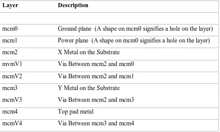
Layer
Description
mcm0
Ground plane (A shape on mcm0 signifies a hole on the layer)
mcm1
Power plane (A shape on mcm0 signifies a hole on the layer)
mcm2
X Metal on the Substrate
mvmV1
Via Between mcm2 and mcm0
mcmV2
Via Between mcm2 and mcm1
mcm3
Y Metal on the Substrate
mcmV3
Via Between mcm2 and mcm3
mcm4
Top pad metal
mcmV4
Via Between mcm3 and mcm4
Apart from defining new layers, the technology file also lays down rules for proper
layout. Classes like Layer Rules class, Physical Rules class and Electrical Rules
class define design rules and constraints.
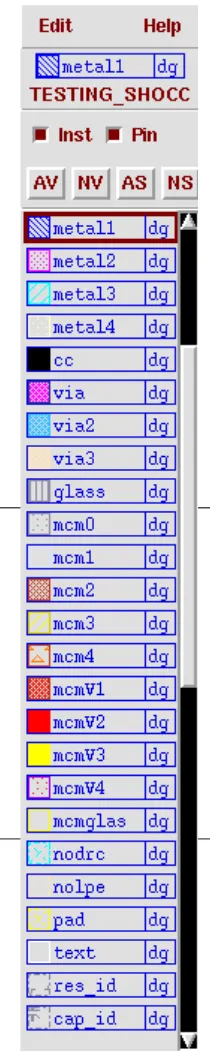
Figure 3 shows the Layer Select Window (LSW) and points
out the new layers that have been added to the already present
layers.
Layers mcm0 and mcm1 are digitized hole layers – i.e. when
extracted, the drawn layers in the layout would actually
represent a hole in layers.
The display.drf (display recourse file) is also written to
represent all of the layers in the tech file. The technology file
and the display resource file together tell the design software
how to display each layer on a specific display device. The
tech file assigns a display packet, by name, to each layer. The
display resource file assigns a display packet definition, with a
display packet name, to each display device.
3.2
TO ADD A LAYER
•
In the layer definition section add the necessary layer name/names, the layer
numbers and the abbreviations
For example
;( LayerName Layer# Abbreviation )
( mcm0 84 mcm0 ) ; mcm layer (ground plane)
( mcm1 85 mcm1 ) ; mcm layer (power plane)
( dummymcm1 94 d_mcm1 ) ; mcm layer
•
In the techLayerPurposePriorities section, mention the layer and the purposes such
as drawing, label, net, pin and boundary.
•
In the techDisplays section, each layer – purpose pair must be associated with a
packet that is defined in the display resource file (display.drf). Also, the
layer-purpose pair must specify the values for five properties that determine their
behavior. The properties are ‘Visible’ (sets the objects visible), ‘Selectable’ (sets
the objects selectable), ‘Changed Layer’ (enables Diva software tracks changes to
objects in incremental verification), ‘Drag’ (enables the objects to be displayed as
it moves) and ‘Valid’ (enables the layer-purpose pair to be displayed on the Layer
Select Window (LSW)).
•
In the layerRules class and the subclass viaLayers, define the layers that conduct
between two other layers.
For example
;( layer1 viaLayer layer2 )
( mcm0 mcmV1 mcm2 )
( mcm1 mcmV2 mcm2 )
( mcm2 mcmV3 mcm3 )‘
•
In the streamLayers subclass, list the stream translation data for the
layer-purpose pairs.
•
The Physical Rules Class has three subclasses, the orderedSpacingRules, the
spacingRules and the mfgGridResolution. In the ordereSpacingRules, the order
of layers is important. In this subclass, we specify the minEnclosure rule that
gives the distance by which an object must be enclosed by another object.
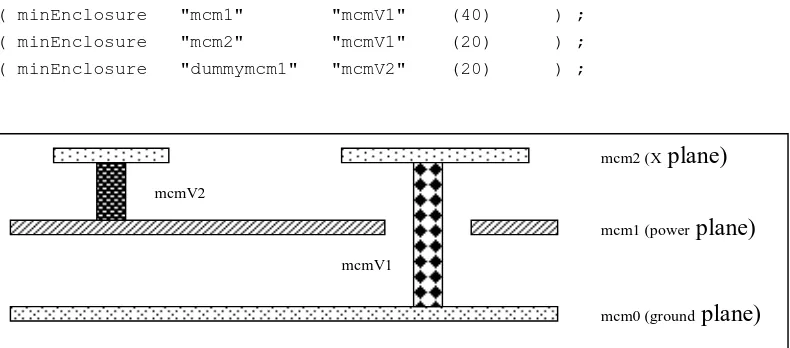
( minEnclosure "mcm1" "mcmV1" (40) ) ;
( minEnclosure "mcm2" "mcmV1" (20) ) ;
( minEnclosure "dummymcm1" "mcmV2" (20) ) ;
As shown in figures 4 and 5, the hole in mcm1, which is the power plane and is
digitised hole
3layer, should enclose mcmV1 by 40 microns. mcm2 should enclose
mcmV1 by 20 microns. The above diagram shows the cross-section of the three
lowest SHOCC layers – the ground plane, the power plane and the X metal plane. It
also shows that if a connection needs to be made from mcm2 (X plane) to the ground
plane, there should be a hole made in mcm1 for the via to pass through.
•
The spacingRules subclass specifies the minNotch (minimum distance between
the outside facing edges of a notch drawn in an object), minSpacing (distance
3
Digitised hole layer indicates that a drawing on the layer would represent a hole in the final circuit.
Figure 4: The Substrate Layer Structure (cross section view)
Figure 5: The Substrate Layer Structure (Top view)
mcm0 (ground
plane)
mcm1 (powerplane)
mcm2 (Xplane)
mcmV1 mcmV2
mcm2
(X plane)
mcm2
(X plane) mcm0 (groundplane)
between objects drawn on the specified layer) and minWidth (minimum width of a
path on the specified layer) values for the layers. Any new layers added would
need to have these values specified. The mfGridResolution subclass specifies
multiple for grid snapping.
•
The Devices class of the technology file defines the devices we would use with
Virtuoso layout. We could also create user-defined devices in the Device class.
The main subclasses that we use in this class are symContactDevice and
symPinDevice. The symContactDevice subclass of the Devices class declares
contact devices. An example of the symContactDevice device statement for the
layers in SHOCC is:
(mcm2_mcm0 mcmV1 drawing
mcm2 drawing
mcm0 drawing (mcm1 drawing 20)
20 20 (1 1 1 1 center center) 20 20 _NA_)
The symPinDevice subclass of the Devices class declares pin devices.
The final technology file is attached as an appendix at the end of the thesis.
3.3
THE DISPLAY RESOURCE FILE (DISPLAY.DRF)
The display resource file, as described above, groups display data in display packets
that it assigns to display devices. A separate display.drf file was created for the
various packets associated with the SHOCC layers. We can have multiple display
resource files at various locations but each one should be named display.drf.
The following lines show the way display.drf is coded:
drDefinePacket(
;( DisplayName PacketName Stipple LineStyle Fill Outline)
( display mcm0 dot4 solid slate slate )
( display mcm1 dot3 solid silver silver.)
( display mcm2 cross solid brown brown )
4 THE DIVA DECK
This section of the thesis deals with the Interactive Verification inside Design
Automation (DIVA) rule decks. There are, primarily, three rule files that have been
created to permit designs that can be fabricated. These rules are Design Rule
Checking (DRC), Extraction rules and Layout versus Schematic (LVS) rules. Each of
the rules are discussed separately in separate subsections in this chapter.
4.1
DESIGN RULE CHECK
This rule file will permit design rule checking of the substrate and solder bumps
against a geometric set of manufacturing design rules. A designer would run the
Cadence Diva package to perform these checks. The rules that have been
implemented in this project are from MicroModule Systems MCM-D Technology Kit.
The kit is provided to support the multi-chip module (MCM) designer to accurately
develop an MCM design. The complete DRC rules list is presented in section 4.1.3 of
this chapter. The rules file that has been written will only check design rules for the
SHOCC layers and not the on chip circuit. For the on chip circuit, previously written
rules were used.
Most of the rules that have been included in the divaDRC.rul file have been specified
DRACULA
4. For this project, these rules were translated to DIVA. Some of the key
expressions in both the languages are discussed in the next section.
4.1.1 Key Features of the DRC rule File
Before writing a design rule check file, we need to consider the various scenarios
within the design that needs to be checked and verified. Some of them like the width
of a path or piece of metal, separation between two like metals, separation between
two different metal layers, etc., are fairly easy to understand – but some of the DRC
checks are subtle and need some understanding of how the layers are represented.
In the rest of this section, some of the DRC scenarios are presented.
4.1.1.1
Separation Between Same Metal Layer
Separation between the same layer can be checked by the drc sep command.
The figure 6 above shows the basic definition of the command.
The example below demonstrates the drc sep command. L25DR2 is the output layer,
The saveDerived command displays the output.
L25DR2 = drc(mcm3 sep < 19.40 )
saveDerived(L25DR2 "mcm3 separation < 19.40")
4.1.1.2
Separation Between Two Different Layers
Separation between two different layers can be done in much the same way except
that this time we need to also figure out whether or not the two layers are overlapping.
4
Dracula is a suite of software products used for verification of integrated circuits – similar to DIVA.
Figure 6: DRC Separation (same layer)
As shown in figure 7, both possibilities must be investigated.
The next piece of code demonstrates how the separation and overlap of two metal
layers can be checked by DRC.
L22DR4A = drc(mcmV2 mcmV4 sep < 30.00 )
saveDerived(L22DR4A "mcmV2 to mcmV4 separation <30.00")
L22DR4B = geomOverlap(mcmV2 mcmV4)
saveDerived(L22DR4B "mcmV2 and mcmV4 overlapping!!")
4.1.1.3
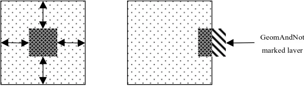
Metal - Via Enclosure
Vias should be completely enclosed by the layers that are been connected by the via.
To check for such design errors, we find out by how much is the edge of the via layer
enclosed by the edge of the metal layer (done by the enc command). If its less than
the specified limit, then an error is registered. We need another command to find out
if the via layer is enclosed by the metal layer on all sides. For that, the geomAndNot
command is used. It marks the area of the via layer that is not overlapped by the metal
layer.Refer figure 8.
The code to represent the above mentioned drc is as follows:
L23DR3A = drc(mcm2Edge mcmV2Edge enc < 19.4)
saveDerived(L23DR3A "mcm2 and mcmV2 enclosure check (mcmV2 should be
enclosed by mcm2 by 19.4 u on each sides)")
L23DR3B = geomAndNot(mcmV2 mcm2)
saveDerived(L23DR3B "mcm2 and mcmV2 enclosure check (mcmV2 is not
completely covered by mcm2)")
Figure 8: DRC Enclosure command
GeomAndNot
4.1.2 Design Rule Check – A Demonstration
In this section, a few
screenshots from Cadence
Virtuoso program show a few of
the DRC errors and the
corresponding messages
followed by another screenshot
that shows the corrected layout.
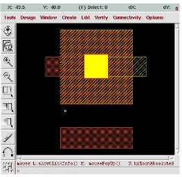
Errors in figure 9
1)
mcmV3 enclosure check
(mcmV3 should be enclosed by
mcm3 by 19.4 u on each sides)
2)
mcm2 separation < 19.40
Figure 9: figure with DRC error
The entry in the log file for the DRC run for the above figures.
DRC started at Wed Dec 20 17:07:49 2000
library: TESTING_SHOCC
cell: DRC_TEST2
view: layout
Rules come from library TESTING_SHOCC.
Rules path is divaDRC.rul.
Inclusion limit is set to 1000.
Running drclayout analysis
Flat mode
Full checking.
DRC started...Wed Dec 20 17:07:49 2000
completed ....Wed Dec 20 17:07:55 2000
CPU TIME = 00:00:00 TOTAL TIME = 00:00:06
**** Summary of rule violation for cell "DRC_TEST2 layout" *****
# errors Violated Rules
1 mcm3 and mcmV3 enclosure check (mcmV3 should be enclosed by...
1 mcm2 seperation < 19.40
2 Total errors found
The entry in the log file for the DRC run for the above figures – after the error was
removed
DRC started at Wed Dec 20 17:11:00 2000
library: TESTING_SHOCC
cell: DRC_TEST2
view: layout
Rules come from library TESTING_SHOCC.
Rules path is divaDRC.rul.
Inclusion limit is set to 1000.
Running drclayout analysis
Flat mode
Full checking.
DRC started...Wed Dec 20 17:11:00 2000
completed ....Wed Dec 20 17:11:06 2000
CPU TIME = 00:00:00 TOTAL TIME = 00:00:06
***** Summary of rule violation for cell "DRC_TEST2 layout" *****
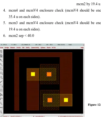
Figure 11 has the following
errors
1.
mcm3 and mcmV3
enclosure check (mcmV3
should be enclosed by
mcm3 by 19.4 u on each
sides)
2.
mcm2 and mcmV3
enclosure check (mcmV3
should be enclosed by
mcm2 by 19.4 u on each
sides)
3.
mcm2 and mcmV3
enclosure check (mcmV3
should be enclosed by
mcm2 by 19.4 u on each sides)
4.
mcm4 and mcmV4 enclosure check (mcmV4 should be enclosed by mcm4 by
35.4 u on each sides).
5.
mcm3 and mcmV4 enclosure check (mcmV4 should be enclosed by mcm3 by
19.4 u on each sides).
6.
mcm2 sep < 40.0
Figure 11: figure with error
The entry in the log file for the DRC run for the above figures.
DRC started at Wed Dec 20 17:28:37 2000
library: TESTING_SHOCC
cell: DRC_TEST
view: layout
Rules come from library TESTING_SHOCC.
Rules path is divaDRC.rul.
Inclusion limit is set to 1000.
Running drclayout analysis
Flat mode
Full checking.
DRC started...Wed Dec 20 17:28:37 2000
completed ....Wed Dec 20 17:28:43 2000
CPU TIME = 00:00:00 TOTAL TIME = 00:00:06
******* Summary of rule violation for cell "DRC_TEST layout" ******
# errors Violated Rules
1 mcm3 and mcmV4 enclosure check (mcmV4 should be enclosed by...
2 mcm3 and mcmV3 enclosure check (mcmV3 should be enclosed by...
1 mcm4 seperation < 20.0
1 mcm2 and mcmV3 enclosure check (mcmV3 should be enclosed by...
1 mcm4 and mcmV4 enclosure check (mcmV4 should be enclosed by...
6 Total errors found
The entry in the log file for the DRC run for the above figures – after the error was
removed
DRC started at Wed Dec 20 17:32:26 2000
library: TESTING_SHOCC
cell: DRC_TEST
view: layout
Rules come from library TESTING_SHOCC.
Rules path is divaDRC.rul.
Inclusion limit is set to 1000.
Running drclayout analysis
Flat mode
Full checking.
DRC started...Wed Dec 20 17:32:26 2000
completed ....Wed Dec 20 17:32:32 2000
CPU TIME = 00:00:00 TOTAL TIME = 00:00:06
***** Summary of rule violation for cell "DRC_TEST layout" *****
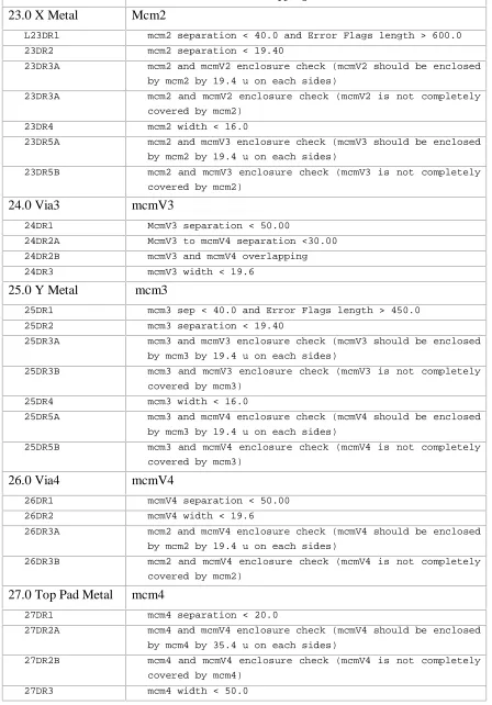
4.1.3 MCM DRC Rule list
This table is a collection of all the DRC rules that have been implemented in the
divaDRC.rul file for the SHOCC – co-layout package.
19.0 Ground Plane
mcm0
19DR1 mcm0 separation < 50.00
19DR2 mcm0 width < 25.00
19DR3A mcmV1 to mcm0 separation <30.00
19DR3B mcmV1 and mcm0 overlapping
19DR4A mcmV2 to mcm0 separation <30.00
19DR4B mcmV2 and mcm0 overlapping
19DR5A mcmV3 to mcm0 separation <30.00
19DR5B mcmV3 and mcm0 overlapping
19DR6A mcmV4 to mcm0 separation <30.00
19DR6B mcmV4 and mcm0 overlapping
20.0 Via1
mcmV1
20DR1 mcmV1 separation < 80.00
20DR2A mcmV1 to mcmV2 separation <30.00
20DR2B mcmV1 and mcmV2 overlapping
20DR3 mcmV1 width < 19.60
20DR4A mcmV1 to mcmV3 separation <30.00
20DR4B mcmV1 and mcmV3 overlapping
20DR5A mcmV1 to mcmV4 separation <30.00
20DR5B mcmV1 and mcmV4 overlapping
21.0 Power plane
mcm1
21DR1 mcm1 separation < 50.00
21DR2 mcm1 width < 25.0
21DR3A mcm1 and mcmV1 enclosure check (mcmV1 should be enclosed
by mcm1 by 30 u on each sides)
21DR3B mcm1 and mcmV1 enclosure check (mcmV1 is not completely
covered by mcm1)
21DR4A mcmV2 to mcm1 separation <30.00
21DR4B mcmV2 and mcm1 overlapping
21DR5A mcmV3 to mcm1 separation <30.00
21DR5B mcmV3 and mcm1 overlapping
21DR6A mcmV4 to mcm1 separation <30.00
21DR6B mcmV4 and mcm1 overlapping
22.0 Via2
mcmV2
22DR1 McmV2 separation < 80.00
22DR2A McmV2 to mcmV3 separation <30.00
22DR2B mcmV2 and mcmV3 overlapping
22DR3 mcmV2 width < 19.6
22DR4B mcmV2 and mcmV4 overlapping
23.0 X Metal
Mcm2
L23DR1 mcm2 separation < 40.0 and Error Flags length > 600.0
23DR2 mcm2 separation < 19.40
23DR3A mcm2 and mcmV2 enclosure check (mcmV2 should be enclosed
by mcm2 by 19.4 u on each sides)
23DR3A mcm2 and mcmV2 enclosure check (mcmV2 is not completely
covered by mcm2)
23DR4 mcm2 width < 16.0
23DR5A mcm2 and mcmV3 enclosure check (mcmV3 should be enclosed
by mcm2 by 19.4 u on each sides)
23DR5B mcm2 and mcmV3 enclosure check (mcmV3 is not completely
covered by mcm2)
24.0 Via3
mcmV3
24DR1 McmV3 separation < 50.00
24DR2A McmV3 to mcmV4 separation <30.00
24DR2B mcmV3 and mcmV4 overlapping
24DR3 mcmV3 width < 19.6
25.0 Y Metal
mcm3
25DR1 mcm3 sep < 40.0 and Error Flags length > 450.0
25DR2 mcm3 separation < 19.40
25DR3A mcm3 and mcmV3 enclosure check (mcmV3 should be enclosed
by mcm3 by 19.4 u on each sides)
25DR3B mcm3 and mcmV3 enclosure check (mcmV3 is not completely
covered by mcm3)
25DR4 mcm3 width < 16.0
25DR5A mcm3 and mcmV4 enclosure check (mcmV4 should be enclosed
by mcm3 by 19.4 u on each sides)
25DR5B mcm3 and mcmV4 enclosure check (mcmV4 is not completely
covered by mcm3)
26.0 Via4
mcmV4
26DR1 mcmV4 separation < 50.00
26DR2 mcmV4 width < 19.6
26DR3A mcm2 and mcmV4 enclosure check (mcmV4 should be enclosed
by mcm2 by 19.4 u on each sides)
26DR3B mcm2 and mcmV4 enclosure check (mcmV4 is not completely
covered by mcm2)
27.0 Top Pad Metal
mcm4
27DR1 mcm4 separation < 20.0
27DR2A mcm4 and mcmV4 enclosure check (mcmV4 should be enclosed
by mcm4 by 35.4 u on each sides)
27DR2B mcm4 and mcmV4 enclosure check (mcmV4 is not completely
covered by mcm4)
27DR3 mcm4 width < 50.0
4.2
EXTRACTION
The process of extraction for the SHOCC layers involves understanding of how the
SHOCC layers have been modeled. As mentioned in the introduction chapter, the
SHOCC lines are modeled as transmission lines. Why we consider long off-chip
interconnects as transmission lines is discussed in the next section. Signal from the
on-chip interconnect is passed on to the substrate through a solder pad. These solder
pads are distributed uniformly throughout the chip surface (There are approximately
13 bump locations in a 0.2 mm radius [7].) The pad layer in SHOCC is represented by
mcm4. As such, whenever metal3 and mcm4 overlap, a solder bump is placed in the
extracted view. Once on the substrate, we have 2 metal layers to propagate the signal
-X route (mcm2) and Y route (mcm3). The two layers are modeled as U elements
(lossy transmission lines). The X and Y models are named UmodelX and UmodelY in
the extraction view.
After traversing the substrate interconnects, the signal hits another solder bump before
it jumps back on the chip. This could be the same chip (intra-chip) or a different chip
(inter-chip for MCMs). The following figure illustrates the SHOCC structure.
4.2.1 Why Transmission Lines?
To obtain accurate chip to chip delays and cross-talk noise estimates, interconnects,
bonding wires and pins should be modeled as transmission lines [10]. This is because
if the interconnect are sufficiently long (its inductance becomes larger) or the circuits
Figure 13: The SCHOCC Paradigm
ON CHIP ON CHIP
SHOCCY SHOCCY
are sufficiently fast such that the rise time of the waveform is comparable to the time
of flight across the line (resulting in a larger L
dIdtand also more crosstalk), the
inductance of the circuit interconnects also becomes important. In these
circumstances, both the distributed inductance and capacitance must be taken into
account. It important to take the inductance into account as it is the cause of the
reverse electromotive force that limits the amount of current that can be applied to the
circuit.
4.2.2 Key Features of the Extraction File
To place the desired components such as the solder bumps and transmission lines in
the extracted view, the divaEXT.rul file was written. This file extracts the on-chip
components such as the transistors and capacitors as well as the off-chip components
like the solder bump and the U element transmission line. Here is a brief description
of how the off-chip devices are extracted.
4.2.2.1
The Solder Bump.
The bump is extracted using the following code:
extractDevice(bump metal3("IN") mcm4("OUT") "bump ivpcell TEST" physical)
Figure 14 shows the extracted view of the BUMP. The R, L and C values for the
bump sub-circuit are given in the section 4.2.3.
The input to the bump is metal 3 and the output is mcm4. The ivpcell cell-view of
bump is looked up in the cell TEST to be placed in the extracted view.
4.2.2.2
The Y model of the U element
The transmission line model for the Y layer is extracted using the following code:
extractDevice( shoccY mcmV4("in") pBulk("refin") groundY("refout") shoccXY
terminal("out") "u1wireSY ivpcell TEST" physical)
The input of this device is mcmV4 and the output is shoccXYterminal.
4.2.2.3
The X model of the U element
The transmission line model for the X layer is extracted using the following code:
ExtractDevice{shoccX shoccXYterminal("in") pBulk("refin") groundX("refout
") shoccXYterminal("out") "u1wireSX ivpcell TEST" physical)
where shoccXYterminal is a derived layer of mcmV3. This layer is the input and the
output to the extracted U model. Again, the ivpcell cell-view from library TEST is
placed in the extracted view. The R, L and C values of the X and Y models are given
in the section 4.2.3.
4.2.2.4
Connecting the Pieces
Now that the bump and the transmission lines have been extracted, the only issue left
is to connect these. GeomConnect statements are used to join the extracted devices.
An example of the geomConnect statement is:
geomconnect(via(mcm4ViamcmV4 mcm4 mcmV4)
via(shoccXYterminal mcm3 mcmV3)
)
where the vias mcm4ViamcmV4 and shoccXYterminal connect the layers mcm4 and
mcmV4 and mcm3 and mcmV3 respectively.
4.2.2.5 Calculate Lengths of Transmission Line
To get the corresponding resistance, capacitance and inductance of the transmission
line elements, the lengths of the elements needs to be determined. The following code
determines the length of the shoccY and saves it in shoccLengthY using the
saveParameter skill function
shoccLengthY=measureParameter( perimeter shoccY 0.5e-6)
saveParameter( shoccLengthY "l")
4.2.3 How Models Are Linked
When a SHOCC line is identified by the extractDevice command, the cell view
U1wireSX ivpcell from library TEST will be put in the extracted view. When a netlist
is desired using HSPICE simulator, Analog Environment looks for the U1wireSX
HSPICE cell view in library TEST. From there the Component Description Format
(CDF) information HSPICE is extracted where the umodelX is specified as the model
name linked to the X line. Analog Environment will look for the file umodelx.m in
the path specified while performing setup. If SpectreS were used for simulation
purposes, we would need to have the SpectreS view.
The umodelx.m file consists of:
.lib umodelX
.MODEL umodelX U level=3
+plev=1
+elev=2
+r11=7.6e2
+cr1=150e-12
+l11=508e-9
.endl umodelX
where the Level = 3 selects the lossy transmission line model. Elev = 2 selects the
pre-computed parameters that allow specification of up to five signal conductors and a
reference conductor. The conductor that we are using here are resistance of the line
per unit length (r11), capacitance of the line with reference to the reference plane per
unit length, (cr1) and the self inductance of the line per unit length (l11). The values
SHOCC interconnects and used MAXWELL Quick 3-D parameter extractor to get the
R, L and C values.
Bumps are linked to the macro SUBCKT in the CDF and a circuit with the R, L and
C values as of those specified in the CDF is created in the extracted view.
The circuit looks like the figure 16 below:
The SUBCKT in HSPICE is as follows:
.SUBCKT &1 1 2
Rbump 1 3 &2
Lbump 3 2 &3
Cbump 2 0 &4
.ENDS &1
The rest of the circuit connects the sub-circuit by nodes 1 and 2. The Resistance is
placed between nodes 1 and 3, the Inductance between nodes 3 and 2 and capacitance
between nodes 0 and 2. The R
bump, L
bumpand C
bumpvalues that have been used for the
bump sub-circuit are taken from [7]. These values have been extracted using
MAXWELL quick 3-D. A more descriptive explanation on how sub-circuits and
transmission line wire models are chosen is provided in the HSPICE manual. The
complete extraction rule file is attached as an appendix.
Figure 16 The Bump Subcircuit
R
bumpL
bumpC
bump0 2 1
4.3
LAYOUT VS SCHEMATIC
The Layout versus Schematic (LVS) program compares two versions of a circuit and
isolates any differences. We can use it to compare two layouts, two schematics, or a
layout and a schematic [8]. For our purpose, we use LVS to compare the extracted
version of the layout and the schematic as drawn by the designer or as provided by a
customer or a third party.
It compares the netlist from the extracted view of the layout with the netlist from the
schematic that has been drawn that represents the layout. The divaLVS rule file is
incorporated with the existing tech files and the diva deck so that simultaneous design
and verification can be performed.
In the SHOCC process, the transmission lines and the bumps are removed for the
LVS process and are replaced by shorts. This is done because the transmission lines
and the solder bumps do not have any effect on the circuit and are just conductors for
the purpose of a net-list match between schematic and layout.
4.3.1 Key Features of LVS
Some of the LVS features that have been utilized in this project are described in this
section. More extensive explanations can be found in the Assura Diva Verification
Reference chapter of the Cadence Openbook reference [8].
4.3.1.1
permuteDevice
The permuteDevice function simplifies a specific type of device depending on the
specific skill function to perform simplification – for example, combine parallel
resistance or series resistance or combine parallel FET. It can also combine MOS
multiple-transistor configurations into single gate-function devices with permutable
inputs. Below is a sample of the permuteDevice command as used in the divaLVS.rul
file.
4.3.1.2
compareDeviceProperty
The compareDeviceProperty function is used to compare properties of devices
matched in the layout and the schematic. This function calls another function that will
compare the two devices. An example of the compareDeviceProperty function as used
in the divaLVS.rul file is:
compareDeviceProperty("res" compareResistor)
compareDeviceProperty("nfet" compareFET)
compareDeviceProperty("pfet" compareFET)
where compareResistor and compareFET are two skill functions that do the
comparing.
4.3.1.3
removeDevice
This function removes the device from the circuit and replaces the device with an
open circuit or a short circuit. This function was used to remove the transmission line
and the bump devices from the extracted view and short the terminals.
The function as used in the divaLVS.rul file is as follows:
removeDevice("u1wireSX" short("in" "out"))
removeDevice("bump" short("in" "out"))
Here, ‘u1wireSX’ and ‘bump’ are removed and the terminals ‘in’ and ‘out’ are
shorted. This is done because in effect, the transmission lines and the bumps make no
difference on how the circuit works.
4.3.1.4
ignoreTerminal
The ignoreTerminal command specifies which terminal types on which device types
to ignore during the comparison. This is done because sometimes all the terminals in a
device are not used in layout but are specified in the schematic, for example, the back
gate of an N channel transistor. This may or may not be connected to power or ground
in the layout but is always connected to the either of the two in schematic. As such it
is best to ignore the back gate in the verification process as it might be erroneous to
include it. An example is presented of the ignoreTerminal command is included here.
ignoreTerminal( "nfet" "B" )
4.3.1.5
Series and Parallel Reduction
Devices that are connected in series or parallel can be combined by series or parallel
reduction. This is done to cut down the number of devices that have to be compared
in series or in parallel. A more detailed explanation of Series and Parallel reduction
can be found in the chapter on LVS in Assura Diva Reference Guide.
4.3.1.6
MOS Reduction
MOS reduction is also possible if the transistors are of the same type and form a
logical function [8].
4.3.2 The Error Files
The LVS program generates files that store the errors that the program encountered.
The error files that are created and a brief description of what errors they store are
mentioned next.
netbad.out
Lists all unmatched nets
devbad.out
Lists all unmatched devices
prunenet.out
Lists all ignored nets
prunedev.out
Lists all ignored devices
mergenet.out
Lists all merged nets
termbad.out
Lists all unmatched terminals
audit.out
Lists all unmatched parameters
A sample output file that was created after running LVS on a design is presented next.
Like matching is enabled.
Net swapping is enabled.
Using terminal names as correspondence points.
Net-list summary for
/afs/unity.ncsu.edu/users/a/akvarma/LVS/layout/netlist
count
15 nets
4 terminals
2 bump
10 pmos
1 u1wireSX
2 u1wireSY
10 nmos
Net-list summary for
/afs/unity.ncsu.edu/users/a/akvarma/LVS/schematic/netlist
count
17 nets
4 terminals
5 pmos
1 u1wireSX
2 u1wireSY
5 nmos
Terminal correspondence points
1 gnd!
2 in
3 out
4 vdd!
The net-lists match.
layout schematic
instances
un-matched 0 0
rewired 0 0
size errors 0 0
pruned 0 0
active 25 15
total 25 15
nets
un-matched 0 0
merged 0 0
pruned 0 0
active 15 17
total 15 17
terminals
un-matched 0 0
matched but
different type 0 0
total 4 4
Probe files from /afs/unity.ncsu.edu/users/a/akvarma/LVS/schematic
devbad.out:
netbad.out:
mergenet.out:
termbad.out:
prunenet.out:
prunedev.out:
I /I4
? Device removed because of user’s ’removeDevice’ request.
I /I7
? Device removed because of user’s ’removeDevice’ request.
I /U2
? Device removed because of user’s ’removeDevice’ request.
I /U3
? Device removed because of user’s ’removeDevice’ request.
I /U1
? Device removed because of user’s ’removeDevice’ request.
audit.out:
devbad.out:
netbad.out:
mergenet.out:
termbad.out:
prunenet.out:
prunedev.out:
+4
? Device removed because of user’s ’removeDevice’ request.
I /+3
? Device removed because of user’s ’removeDevice’ request.
I /+2
? Device removed because of user’s ’removeDevice’ request.
I /+1
? Device removed because of user’s ’removeDevice’ request.
I /+0
? Device removed because of user’s ’removeDevice’ request.
5 CASE STUDY – DRIVER RECEIVER CIRCUIT
To demonstrate that the designed tool-set works satisfactorily, a driver and a receiver
(which is simply an inverter) circuit were connected via off chip MCM layers. Figure
17 (modified from Afonso, et al [7]) shows the Driver – Receiver circuit and where
the interconnect attaches the two.
Signal from the driver was brought onto the substrate. The signal was propagated
using the X and Y layers and was brought back on the chip to be connected to the
Figure 17: Driver and Receiver circuit
Driver
Receiver
SHOCC interconnect that
has replaced the long on-chip
interconnect
Long on-chip interconnect
inverter. This circuit was checked for design rule errors, extracted and then the
extracted netlist matched against the schematic netlist thus checking for any Layout
Versus Schematic errors. This chapter discusses in detail the case study of the driver
and the receiver circuit.
5.1
LAYOUT AND DRC
Layout was done by creating an instance of the driver (that was laid out previously for
another project) and an instance of an inverter. The output of the driver is connected
to the input of the inverter via the substrate layers. Metal 3 at the output of the driver
is laid out in such a way such that it overlaps mcm4 layer (a SHOCC top pad layer).
From there, the signal is passed through to mcm3 (which is the Y Plane on the
substrate) via the contact, mcmV4. The signal is then passed on to mcm2 (which is
the X Plane on the substrate) via the contact layer mcmV3. The signal is then brought
back to mcm3 from where it is connected to mcm4 and back to metal 3 to the input of
the inverter. The layout described above is drawn out in figure 18. The two figures
either side indicate the location of the driver and the inverter. The two figures
following the complete layout are the figures of the driver and the inverter layout.
The driver and the inverter are subjected to individual design rule checks. Once they
are connected together with the SHOCC layers, they are again tested for design rule
violation. Presented below are the results of the individual DRC runs for the driver
and the inverter and then the result of the combined DRC run.
Log file entry for DRC run for driver:
DRC started at Wed Feb 21 12:23:05 2001
library: DESchip
cell: outputdriver2
view: layout
Rules source is a simple file.
Rules path is /afs/eos.ncsu.edu/dist/cad445/local/techfile/divaDRC.rul.
Inclusion limit is set to 1000.
Running drclayout analysis
Flat mode
Full checking.
DRC started...Wed Feb 21 12:23:05 2001
completed ....Wed Feb 21 12:23:12 2001
CPU TIME = 00:00:00 TOTAL TIME = 00:00:07
** Summary of rule violation for cell "outputdriver2 layout" **
Total errors found: 0
Log file entry for DRC Run for the inverter
DRC started at Wed Feb 21 12:24:46 2001
library: TEST_SHOCC_3
cell: inv_hp
view: layout
Rules source is a simple file.
Rules path is /afs/eos.ncsu.edu/dist/cad445/local/techfile/divaDRC.rul.
Inclusion limit is set to 1000.
Flat mode
Full checking.
DRC started...Wed Feb 21 12:24:46 2001
completed ....Wed Feb 21 12:24:52 2001
CPU TIME = 00:00:00 TOTAL TIME = 00:00:06
******* Summary of rule violation for cell "inv_hp layout" *******
Total errors found: 0
Log file entry for DRC Run for the entire circuit
DRC started at Wed Feb 21 12:26:30 2001
library: TEST_SHOCC_3
cell: SHOCC_TEST
view: layout
Rules source is a simple file.
Rules path is ~/erl/SHOCC/final_code/divaDRC.rul.
Inclusion limit is set to 1000.
Running drclayout analysis
Flat mode
Full checking.
DRC started...Wed Feb 21 12:26:30 2001
completed ....Wed Feb 21 12:26:36 2001
CPU TIME = 00:00:00 TOTAL TIME = 00:00:06
******* Summary of rule violation for cell "SHOCC_TEST layout" *****
Total errors found: 0
![Figure 2: A High performance SHOCC IC (reference [7])](https://thumb-us.123doks.com/thumbv2/123dok_us/1295878.1162157/15.612.115.483.320.605/figure-high-performance-shocc-ic-reference.webp)