Volume No.02, Issue No. 11, November 2014 ISSN (online): 2348 – 7550
EFFICIENT HIGH SPEED ADDERS FOR 4-BIT
MICROPROCESSOR
Mr. Babu T Chacko
Asst. Professor, Department of Electrical and Electronics, Viswajyothi College of Engineering and
Technology, Vazhakulam, Muvattupuzha, Ernakulam, Kerala, (India)
ABSTRACT
This paper primarily deals with the development of a Verilog model of 4-bit Microprocessor from basic gates
and the construction of high speed adder circuits using Xilinx ISE 8.1i. The designs are implemented on Field
Programmable Gate Array (FPGA) to analyze the design parameters. The motivation behind this investigation
is that an adder is the basic building block of the Arithmetic Logic unit (ALU) and would be a limiting factor in
the performance of the Central Processing Unit. In this research article we have simulated and synthesized the
various adders like Ripple Carry Adder, Carry Look Ahead Adder and Carry Skip Adder by using Verilog and
Xilinx ISE 8.1i. The Verilog codes for the architecture were synthesized using Xilinx ISE 8.1iand targeted for
Xilinx Spartan 3E FPGA. The functionality of high speed adders are verified and parameters like area and
speed is analyzed.
Keywords: Carry Look Ahead Adder, Carry Skip Adder Field Programmable Gate Array, Ripple
Carry Adder.
I. INTRODUCTION
MICROPROCESSOR is a multipurpose, programmable, clock-driven, register-based electronic device that reads
binary instruction from a storage device called memory; accepts binary data as input & processes data according
to those instructions and provides results as output. The designed model in this paper is such that it will be
capable of executing an assembly-language program written using the instruction set. Here in this paper we first
designed the processor with Ripple Carry Adder [1]. In the next stage of design Carry Look Ahead Adder and
Carry Skip Adders were designed and new 4-bit processor units were also designed with these high speed adders
[6]. We have designed a 4-bit processor considering the ease of design and this unit can be expanded to 8-bit,
16-bit, 32-bit etc. easily.
II. DESCRIPTION
The entire 4-bit microprocessor design is done in different stages [2]. The different stages involved in the design
are described below.
2.1 GATE Implementations:
In this stage the behavioral description of XOR, AND, OR and NOT gate are written and tested in test benches.
2.2 The 4-bit Full Adder:
In this stage structural description of a 4-bit full adder, either using top-bottom or bottom-up approach is written
Volume No.02, Issue No. 11, November 2014 ISSN (online): 2348 – 7550
numbers and carry input as inputs and gives one 4-bit number and carry as outputs. The main issue with thisadder is that carry has to propagate through all the stages and propagation delay is more.
Figure 2.1: Ripple Carry Adder
2.3 The 4-bit ALU:
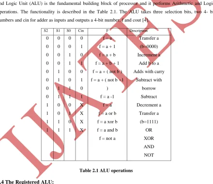
There are three selection bits : S2,S1 and S0 and hence support 8 operations. It uses adder of stage 2. Arithmetic
and Logic Unit (ALU) is the fundamental building block of processor and it performs Arithmetic and Logic
operations. The functionality is described in the Table 2.1. The ALU takes three selection bits, two 4- bit
numbers and cin for adder as inputs and outputs a 4-bit number, f and cout [4].
Table 2.1 ALU operations
2.4 The Registered ALU:
This introduces clocked procedures for register modeling. The output signals f and cout from ALU of stage 3 is
synchronized to a rising edge of the clock. An active low asynchronous reset signal controls initialization of
these output signals.
2.5 The Instruction Decoder:
The instruction decoder is the part of the CPU that converts the bits stored in the instruction register or in CPUs
S2 S1 S0 Cin F Description
0 0 0 0 0 0 0 0 1 1 1 1 0 0 0 0 1 1 1 1 0 0 1 1 0 0 1 1 0 0 1 1 0 1 0 1 0 1 0 1 0 1 0 1 X X X X
f = a
f = a + 1
f = a + b
f = a + b + 1
f = a + ( not b )
f = a + ( not b +1
)
f = a -1
f = a
f = a or b
f = a xor b
f = a and b
f = not a
Transfer a
(b=0000)
Increment a
Add b to a
Adds with carry
Volume No.02, Issue No. 11, November 2014 ISSN (online): 2348 – 7550
input, an instruction set comprising of a 3-bit opcode and two 4-bit operands. The instruction set is describedbelow in the table 2.1.
2.6 16 X 4 RAM Model :
A random-access memory device allows data items to be read and written in roughly the same amount of time
regardless of the order in which data items are accessed.
The input ports are :
addr ( 4-bit vector ), datain ( 4-bit vector )
csn ( 1 bit ): chip select, it is 0 when memory is in use
rwn ( 1 bit ) : 1 = read memory; 0 =write memory
The output port :dataout ( 4-bit vector ) : Output data from RAM when in read mode.
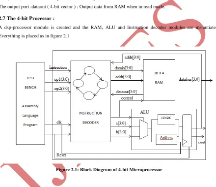
2.7 The 4-bit Processor :
A dsp-processor module is created and the RAM, ALU and Instruction decoder modules are instantiated.
Everything is placed as in figure 2.1
Figure 2.1: Block Diagram of 4-bit Microprocessor
2.8 Assembly Language Programs :
A file containing assembly language program for the processor is created. A small compiler in C/C++ is
developed which will translate this program into a test-bench program in which this instructions are input to the
instruction decoder of figure 2.1 with necessary timings between instructions
2.9 Synchronous RAM with Bidirectional Data :
A clock and reset signal will be added into the RAM model already designed. The code has to be modified to
sync up the data input and output with the clock. The datain and dataout signals will have to be combined into
Volume No.02, Issue No. 11, November 2014 ISSN (online): 2348 – 7550
III.
DESIGN
OF
ADDERS
So far we have completed the design of 4-bit processor comprising of ALU unit with Ripple Carry Adder, RAM
and Instruction Decoder. Now we are going to design more efficient adders Carry Look Ahead Adder and Carry
Skip Adder.
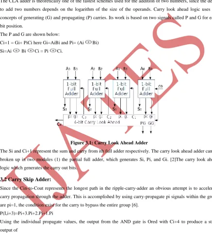
3.1 Carry Look Ahead Adder
:
The CLA adder is theoretically one of the fastest schemes used for the addition of two numbers, since the delay
to add two numbers depends on the logarithm of the size of the operands. Carry look ahead logic uses the
concepts of generating (G) and propagating (P) carries. Its work is based on two signals called P and G for each
bit position.
The P and G are shown below:
Ci+1 = Gi+ PiCi here Gi=AiBi and Pi= (Ai Bi)
Si=Ai Bi Ci = Pi Ci.
Figure 3.1: Carry Look Ahead Adder
The Si and Ci+1 represent the sum and carry from ith full adder respectively. The carry look ahead adder can be
broken up in two modules (1) the partial full adder, which generates Si, Pi, and Gi. [2]The carry look ahead
logic which generates the carry out bits.
3.2 Carry Skip Adder:
Since the Cin-to-Cout represents the longest path in the ripple-carry-adder an obvious attempt is to accelerate
carry propagation through the adder. This is accomplished by using carry-propagate pi signals within the group
are pi=1, the condition exist for the carry to bypass the entire group [6].
P(I,i+3)=Pi+3.Pi+2.Pi+1.Pi
Using the individual propagate values, the output from the AND gate is Ored with Ci+4 to produce a stage
output of
Carry = Ci+4 +P(i,i+3).Ci
As shown in the figure, if P(i,i+3)=0, then the carry-out of the group is determined by the value of Ci+4.
However, if P(i,i+3)=1, then the carry-in bit is Ci=1, then group carry-in is automatically send to the next group
of adders. The name “carry-skip” is due to the fact that if the condition P(I,i+3).Ci is true and then the carry-in
Volume No.02, Issue No. 11, November 2014 ISSN (online): 2348 – 7550
Figure 3.2: Carry Skip Adder
IV.
CONCLUSION
In this paper we have designed the Verilog model of a 4-bit processor and synthesized in Xilinx ISE
8.1i.Various adders like Ripple Carry Adder, Carry Look Ahead Adder and Carry Skip Adders were designed. It
is found that the combinational delay path is reduced in case of adders Carry Look Ahead and Carry Skip Adder
as compared to that of Ripple Carry Adder. The adders are also synthesized in Xilinx ISE 8.1i. The reduction in
delay path is more significant in case of higher order bit adders like 8-bit, 16-bit, 32-bit etc. From the timing
summary analysis of 8-bit adder units- Ripple Carry Adder, Carry Look Ahead Adder and Carry Skip Adder it
was found that the combinational delay path of Carry Look Ahead Adder is reduced significantly since the level
of logic gates is reduced. . The reduction in delay path is more significant in case of higher order bit adders like
8-bit, 16-bit, 32-bit etc.
REFERENCES
[1] Bruce Shriver and Bennett Smith, “The Anatomy of a High- Performance Microprocessor”, IEEE
Computer society Press, Los Alamitos, CA, 1998.
[2] James M. Feldman and Charles T. Retter, “Computer Architecture” McGraw-Hill, New York, 1994.
[3] Carl Hamarcher, Zvonko Vranesic and Safwat Zaky, “Computer Organization”, McGraw-Hill, New York,
2002
[4] BehroozParhami, “Computer Arithmetic”, Oxford University Press, New York, 2000. A comprehensive, in
depth treatment of the subject.
[5] Xilinx, Using Block RAM in Spartan-3 FPGAs, Dual-Port Block Memory Core v6.3,. www.xilinx.com.
[6] Prashant Gurjar, Rashmi Solanki, Pooja Kansliwal, “VLSI implementation of adders for high speed ALU ” ,