www.adv-radio-sci.net/4/225/2006/ © Author(s) 2006. This work is licensed under a Creative Commons License.
Radio Science
Yield-improving test and routing circuits for
a novel 3-D interconnect technology
M. Bschorr1, H.-J. Pfleiderer1, P. Benkart2, A. Kaiser2, A. Munding2, E. Kohn2, A. Heittmann3, H. H ¨ubner3, and U. Ramacher3
1University of Ulm, Microelectronics Department, Albert-Einstein-Allee 43, 89081 Ulm, Germany 2University of Ulm, Department of Electron Devices and Circuits, Germany
3Infineon Technologies AG, Germany
Abstract. This work presents a system to increase the yield of a novel 3-D chip integration technology. A built-in self-test and a routing system have been developed to identify and avoid faults on vertical connections between different stacked chips. The 3-D technology is based on stacking sev-eral active CMOS-ICs, which have through-substrate elec-trical contacts to communicate with each other. The ex-pected defects of these vias are shorts and resistances that are too high.
The test and routing system is designed to analyze an ar-bitrary number of connections. The result ist used to gain information about the reliability of the new 3-D processing and to increase its yield. The circuits have been developed in 0.13µm technology, one chip has been fabricated and tested, another one is in production.
1 Introduction
The recent development in micro- and nanotechnology is not sufficient to meet all the needs of upcoming electronic appli-cations. For instance, the area of mobile communications demands a steadily increasing number of functions which leads to more and more energy and area consumption of in-tegrated circuits. The shrinking of the technology alone is not able to compensate these drawbacks. Typical tasks are en- and decoding of video signals, multi-mega-pixel cam-eras, interactive mobile games or visual telephony. Stan-dards like UMTS, WLAN or HiperLAN offer the required bandwidth and have to be included in current and future portable terminals. Many complex applications, e.g. in the field of video signal processing or human-machine interfaces cause a “power crisis”, which makes the realization difficult. The situation is exacerbated by the limited physical dimen-sions of a few square centimeters for integrated circuits.
An-Correspondence to: M. Bschorr
other difficulty is presented by complex system architectures that require circuits in different material systems, like opto-electronics or HF-tranceivers. The solution of embedded technologies cause unacceptable production costs and some even reliability problems. Thus, a new solution for the men-tioned problems has to be found.
A possible way out of this dead end is a new kind of 3-D integration of integrated circuits. It offers the possibility of distributing the connections between stacked chips freely, thus gaining in parallelism and consequently in transmission bandwidth. At the same time the length of interconnect lines and therefore power dissipation can be reduced considerably. Different material systems do not propose difficulties any more, because they can be produced and tested separately as a single chip, and then assembled on the 3-D stack. The inte-gration of sensors, memory, processors or analogue circuits benefits from this approach.
Nevertheless this new technique, particularly the process-ing of vertical contacts, introduces new problems. The sprocess-ingle chips are ”known good dies”, tested with standard test algo-rithms (Abramovici et al., 1990). The task at hand was now to develop a test method specialized in the new 3-D vias. Furthermore a dynamic routing system had to be designed to ensure the overall reliability of the system, even though some of the vertical connections might not be working. The defect model used consists of short to ground,VDD or the
next neighbor. In addition to that, a high resistance up to interrupted connection is considered.
••
picture
thinned Si-substrate soldering pre-metalization
contact pads and routing
through-chip via 1st layer
(bottom substrate) 2nd layer (e.g. neural net) nthlayer
sensor (CMOS) top layer
Fig. 1. Schematic description of the 3-D chip stacking
2 3-D chip stacking
The goal of the project is to fabricate a stack of chips that introduces a new 3-D connection and packaging technology. The application to be realized is video processing based on pulse-coded neural nets. The 3-D technology will provide the very demanding connection density for the neural net.
The individual parts of the system consist of mixed ana-logue/digital integrated circuits. Especially the analogue im-plementation of the integrate-and-fire neurons enable the sys-tem to process video signals in a robust manner. The use of moderate operating frequencies leads to the desired low power consumption (Schreiter et al., 2004).
Figure 1 shows a schematic description of 3-D chip stack providing feature detection using pulse-coded neural nets (Heittmann et al., 2002).
3 Technology
A whole new processing scheme was developed that not only provides for the electrical connections between the stacked chips, but also accounts for the mechanical stability of the whole stack (Munding et al., 2004). The starting point are CMOS chips. This standard processing is not altered, 3-D processing starts after their fabricating and testing.
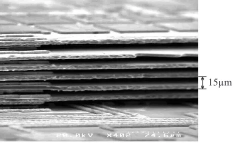
Firstly, the substrate of the silicon CMOS chips has to be thinned to about 10µm. This step leads to an aspect ratio for the desired vertical connections of 1:2, which is important for the following etching and electroplating. Holes of 5µm diameter are then etched, isolated in respect to the substrate and filled with copper galvanically. To enable the soldering of different chips on top of each other, the bottom and top of each chip are coated with copper and tin. The soldering step (SOLID Huebner et al., 2002) takes into account, like the other 3-D processing steps, the temperature budget of the CMOS chips. A REM inspection of a fabricated chip stack is shown in Fig. 2. There, an unthinned bottom chip on which six thinned chips are soldered can be seen.
15µm
Fig. 2. REM inspection of a seven-chip 3-D stack
Table 1. Extracted values in the via model
capacitance per unit surface Csubstrate0 ≈ [0,2]f F
µm2
substrate capacitance (Fig. 3) Csubstrate= [100]f F
coupling capacitance Ccoup= [1]f F
via resistance Rvia<[5]
3.1 Modelling the vias
The materials set by CMOS technology lead to a model for vertical connections dominated by capacitances. Figure 3 shows that caused by the relatively low oxide thickness of less than[1]µm between copper lines and the p+layer on the bottom of the substrate, a notable capacitanceCsubstrateis created. This can be approximated by a parallel plate type ca-pacitor. The influence of the capacitance inside the vias can be neglected, because of the high resistance of the almost un-doped substrateRSi. Likewise the capacitive coupling effects
have not to be taken into consideration because the distances are magnitudes higher. The results are given ina Table 1. Estimations considering inductances delivered values that do not affect the signals, given the low operation frequency of the system.
3.2 Requirements of the circuits
C C
R
VDD TG TG VDD
TG test 1
TG test 2
R C C R
coup
via
substrate
Si Si Si
Si
p+ layer
Fig. 3. Schematic description, model und test approach of two
ad-jacent vias
fault probability of a single viap
overall
chip
stack
yield
0
0,0006 0,0004
0,0002
0 0,0008
0,2 1 0,8
0,001 0,6
0,4
Pyield=p
10000
Fig. 4. Overall yield of a chip utilizing 10000 unreliable contacts
4 Unreliable connection and yield
Even if one element of a complex system is slightly unreli-able, the overall yield decreases dramatically if this element is used several thousand times in the system. As can be seen in Fig. 4, the yield of a chip stack using 10000 vias rapidly converges towards zero if the fault probability of a single via increases.
Therefore a way of testing the connections has to be found. Only after the test, a dynamic routing circuit can determine a way so that all signals are transmitted through working vias. The proposed system can be seen in Fig. 5.
5 Test approach and circuit
Known and established test algorithms (Abramovici et al., 1990) require too much circuitry, because they do not match the fault model at hand. Their application is the testing of complex integrated circuits. A specialized scheme has been developed. Figure 6 shows that, if the connections between chip A and B have to be tested, circuitry on both chips is needed.
During the testing, the circuits on chip A send a voltage impulse through the vias. If chip B can correctly receive the
Via-test Dynamic routing
Neural Net
Neural Net
Signals to transmit
available vias
Via-test Dynamic routing Chip(n+1)
3D connections
Chip(n)
Signals to transmit
Neural Net
Neural Net
Fig. 5. Test and dynamic routing system overview
CONTROL
A A A A
A A A A
B B B B
B B B B
Fig. 6. Example: a 2 by 4 via-field test
test signal, the result is stored: that particular contact works. If not, the default value is kept: the contact is faulty. The impulse is not sent through all vias at the same time. That way shorts to next neighbors can be identified.
As a last step, the gathered information now stored on chip B is sent back to chip A. This is essential, as only when the same information is available on both sides, the routing sys-tem described in Sect. 6 is able to avoid faulty connections. In addition to that, the test results can be read out serially for external analysis of the statistics of occurring errors.
The BIST was designed in a[0.13]µm technology. Most of the logic uses transfer transistors and transmission gates to meet the requirements mentioned in Sect. 3.2. As can be seen in Fig. 6, an additional control block is needed on one side of the vias under test. For more information about the test circuit, refer to Bschorr et al. (2005).
6 Routing approaches and circuits
TD multiplexer
TD demultiplexer input signals
output signals Routing
Routing
upper chip
lower chip
test
result systemclock
Fig. 7. Block diagram of the routing circuit
than signals have to be transmitted, or not. In the second case the system does not have built-in redundancy and there-fore a time division multiplexing (TDM) scheme has to be introduced to transmit several signals through one connec-tion. Both approaches subdivide the task into groups of vias to limit the use of logic and horizontal interconnect lines to an amount feasible for the application.
If more vias than needed are on-hand, the circuit that iden-tifies possible routes through the unreliable vertical connec-tions is straightforward. Basically the circuit consists of a multiplexer and controlling combinatorial logic that decodes the information found by the test circuit. The same circuitry is needed on the second chip to channel the signals to the ap-propriate receiver. This whole system works asynchronously. If TDM has to be introduced, more area consuming cir-cuits are needed. The most severe change is that the sys-tem now works synchronously using a global clock signal. To minimize the delay effect caused by TDM, the clock frequency has to be chosen comparatively high. Figure 7 shows an exemplary block diagram of the developed circuits. the routing system was also designed using a [0.13]µm technology.
Under the assumption of evenly distributed defects with the probabilityp, the yield of the whole systemPyieldcan be calculated. The combinatorial equation used is
Pyield=
Nmax
X
n=0 (Nvias
n )pn(1−p)(Nvias−n) !Nsections
,
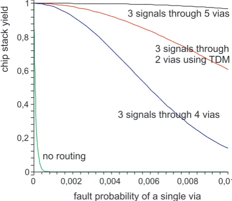
whereNmaxrepresents the maximum acceptable number of errors per section,Nviasthe number of vias used per section andNsectionsthe number of sections in the chip stack. The yield improvements achieved by different routing concepts are shown in Fig. 8. As expected one can see that without TDM, the more redundancy is spent, the better the system yield becomes. Applying TDM leads to another trade-off.
0,006 1
0,008 0,8
0,004 0
0,2
0,002 0
0,6
0,01 0,4
fault probability of a single via
chip
stack
yield
no routing
3 signals through 4 vias 3 signals through 5 vias
3 signals through 2 vias using TDM
Fig. 8. Dynamic routing: improving the overall yield of a chip stack
transmitting 10000 signals vertically
The higher the amount of signals per connection is chosen, the fewer vias are needed for the transmission, without com-promising the reliability. The drawback of this solution is the increasing delay caused by the multiplexing scheme. Here the system designer must decide, what delay is acceptable for the application at hand.
7 Summary and outlook
Vertical inter-chip connections of a technology still under de-velopment can be expected to be defect-ridden. To overcome this problem test and dynamic routing circuits were devel-oped that automatically test the unreliable connections and route the signals through working vias. The whole system was designed and simulated using[0.13]µm technology and SPICE-based simulation. A prototype chip containing the test scheme was fabricated and tested, a second is in pro-duction. Our future work will consist of combining test and routing circuits to show that the developed system offers a 3-D-communication construction kit which allows designers to use the new technology and improve the overall yield by utilizing a routing scheme fit for the application.
Acknowledgements. The authors want to thank the German min-istry of education, science, research and technology (BMBF) for the funding in the context of the project Vision IC (F¨orderkennzeichen 01M3127B).
References
Abramovici, M., Breuer, M. A., and Friedman, A. D.: Digital Sys-tems Testing and Testable Design, IEEE Press, New York, 1990. Bschorr, M., Pfleiderer, H.-J., Munding, A., Kaiser, A., Benkart, P., Kohn, E., Heittmann, A., Hbner, H., and Ramacher, U.: Eine Test- und Ansteuerschaltung fr eine neuartige 3D Verbindung-stechnologie, Advanves in Radio Science, 3, 305–310, 2005. Heittmann, A., Ramacher, U., Matolin, D., Schreiter, J., and
Schffny, R.: An Analog VLSI Pulsed Neural Network for Im-age Segmentation Using Adaptive Connection Weights, ICANN 2002 Proceedings, Madrid, Spain, 2415, 1293–1298, 2002.
Huebner, H., Eigner, M., Gruber, W., Klumpp, A., Merkel, R., Ramm, P., Roth, M., Weber, J., and Wieland, R.: Face-to-Face Chip Integration with Full Metal Interface, Proc. Advanced Met-allization Conference AMC 2002, p. 53, 2002.
Munding, A., Kaiser, A., Benkart, P., Bschorr, M., Heittmann, A., Hbner, H., Pfleiderer, H.-J., Ramacher, U., and Kohn, E.: Chip Stacking Technology for 3D-Integration of Sensor Sys-tems, HETECH 2004, 13th European workshop on heterostruc-ture technology, October 2004, Heraklion, Greece, 2004. Schreiter, J., Ramacher, U., Heittmann, A., Matolin, D., and