CRAY-1®
COMPUTER SYSTEMS
c:
RESEARCH, INC.
CRAY-1®
COMPUTER SYSTEMS
,
HARDWARE REFERENCE MANUAL
HR-0004
RECORD OF REVISION RESEARCH. INC. PUBLICATION NUMBER HR-0004
Each time this manual is revised and reprinted, all chan~es issued against the previous version in the form of change packets are incorporated into the new version and the new version IS assigned an alphabetic level. Between reprints, changes may be issued against the current version in the form of change packets. Each change packet is assigned a numeric designator, starting with 01 for the first change packet of each revision level.
Every page changed by a reprint or by a change packet has the revision level and change packet number in the lower righthand corner. Changes to part of a page are noted by a change bar along the margin of the page. A change bar in the margin opposite the page number indicates that the entire page is new; a dot in the same place indicates that information has been moved from one page to another, but has not otherwise changed.
Requests for copies of Cray Research, Inc. publications and comments about these publications should be directed to: CRAY RESEARCH, INC.,
1440 Northland Drive,
Mendota Heights, Minnesota 55120
Revision Description
January 1976 - Original printing
A r,1ay 1976 - Repri nt wi th revi s i on
A-01 September 1976 - Corrections to pages 3-20, 3-27, 4-9, 4-10, 4-28, 4-36, 4-43, 4-55, and 4-57.
B October 1976 - Reprint vlith reV1Slon. Addition of floating point range error detection, vector floating point error, and error correction.
8-01 February 1977 - Changes to exchange pckage, additions to instructions 152 and 153, corrections to syndrom bit
description, corrections to instruction summary, appendix D.
8-02 July 1977 - Corrections and changes to pages xi, 2-3, 3-19
through 3-28.1, 3-31, 3-34, 3-36, 3-38, 4-14 through 4-17, 4-54, 4-68,5-1, 5-3,5-4,5-6,6-2, A-4, D-1 through D-4.
C November 1977 - This printing obsol~tes revision B. Features added include 8-bank phasing and I/O master clear procedure. Chart tape reflects only changes introduced with this revision.
C-01 April 1978 - This change packet changes the nomenclature for two flags in the exchange package (page 3-37) and corrects technical errors on pages 2-11, 4-71, 5-6, 6-5, and A-3.
C-02 July 1978 - This change packet documents changes to the physical description of the CRAY-l Computer System. Changes are all in section 2.
Revision Description
E May 15, 1979 - Reprint with reV1Slon. This printing corrects the description of the multiply algorithm and adds descriptions of various standard options (i.e., vector population
instructions, programmable clock interrupt, and monitor mode interruptl. In addition, sections 5 and 6 have been rewritten. Revision E obsoletes versions C and 0 of this publication.
E-01 May, 1980 - This change packet documents changes to the multiply functional unit that supports symmetrical multiply, documents CAL instruction changes, and corrects miscellaneous technical errors. Changes are noted by change bars.
I
CONTENTS
1. INTRODUCTION . . . . . COMPUTATION SECTION MEMORY SECTION . . . .
INPUT/OUTPUT SECTION . VECTOR PROCESSING . .
2. PHYSICAL ORGANIZATION
INTRODUCTION . MA I NFRA}1E . .
Modules
Clock . . Power supplies
PRIMARY POWER SYSTEM . COOLING . . . . MAINTENANCE CONTROL UNIT . FRONT-END COMPUTER . . . EXTERNAL INTERFACE . . MASS STORAGE SUBSYSTEM .
3. COMPUTATION SECTION
INTRODUCTION . . . . . REGISTER CONVENTIONS OPERATING REGISTERS
V registers . .
.
.
.
.
. .
. .
. .
.
.
.
.
V register reservations . .Vector control registers VL register
VM register S registers T registers A registers B registers
· . 1-1
· 1-4
1-5 1-5
· . 1-6
2-1
· 2-1 2-1 2-1
2-4 2-5 2-5
· 2-6
· 2-6 2-7
· 2-7 · . 2-8
· 3-1
· 3-1
3-3 · . 3-3
· . 3-4
· . 3-5
· . 3-6 3-6
· 3-6 · . 3-7
3-8
I
FUNCTIONAL UNITS 0 0 . ' 0 If • • • • • • o 3-10
3-11 3-11 3-11 Address functional units
Addres~ add unit 0 0
Address multiply unit, Scalar functional units
Scalar add ~nit 0 0 , 0
Scalar shift unit
. . . '.
o 0 0 3-12' 00 • 0 3-12 o 3-12
Scalar logical unit 3~13
Population/leading zero count unit 0 • 3-13
Vector functional units . 0 0 0 0 0 0 • • 0 0 3-13
Vector functional unit reservation 0 • 0 • • • 0 0 ' '3-13
'Recursive characteristic of vector functional units o . 3-14
Vector add unit 0 0 • 0 • 0 0 0 0 0 3-17
Vector shift unit 0 0 0 0 • 3-17
Vector logical unit 0 0
Vector population count unit. Floating point functional units.
Floating point add unit
Floating point multiply unit. Reciprocal approximation unit
.
'.
.
· 3-17 3-18 · 3-18
o 3-18
· 3-19
o 0 0 3-19
ARITHMETIC OPERATIONS 3-20
. 3-20 . 3-21
Integer arithmetic
'.
.
.
Floating point arithmetic 0 0
Normalized floating point . 0 • • • • • • 0 • 3-22
Floating point range errors 0 • • • 0 3-22
Floating point add unit . 0 • 3-23
Floating point multiply unit 0 • • 0 • • 0 • 3-23
Floating point reciprocal approximation unit 0 0 • 3-23
Double precision numbers 0 • • • • • 3-24
Addi t i on algor; thm 0 0 • 0 • 3-24
Multiplication algorithm 0 • ' . • 3-25
Division algorithm o 3-30
4.
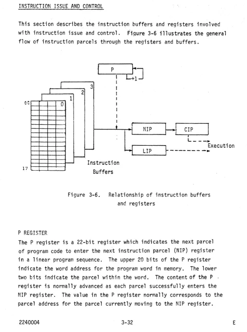
INSTRUCTION ISSUE AND CONTROL P register .
CIP register NIP register LIP register
Instruction buffers
EXCHANGE MECHANISM XA register. M register . F register . Exchange package
Memory error data . . . . Active exchange package . . . . Exchange sequence . . . .
Initiated by dead start sequence .
Initiated by interrupt flag set . . . . Initiated by program exit . . . .
Exchange sequence issue conditions . . . Exchange package management
MEMORY FIELD PROTECTION BA regi ster . . LA register
DEAD START SEQUENCE
INSTRUCTIONS . . .
INSTRUCTION FORMAT .
. .
. . .
.
.
. .
. . . .
.
.
Arithmetic, logical format Shift, mask format
Immediate constant format Memory trans fer format Branch format . . . . .
SPECIAL REGISTER VALUES
3-32
· . 3-32
· . 3-33
· . 3-33
· . 3-34 3-34
3-37
· . 3-37
· . 3-37
· . 3-39
· 3-40
· . 3-41
· . 3-42
· 3-42
· 3-43
· . 3-43
· . 3-43 3-44
3-45
. . . 3-46
· . 3-47 3-47
· . 3-47
· . 4-1
· . 4-1
· 4-1 4-2
· . 4-2
· 4-3 . . . . 4-4
I
I
INSTRUCTION ISSUE . . .
INSTRUCTION DESCRIPTIONS .
4-5
· 4-6 4-7 000000
001 i j k 0014j k 0020xk 0021xx 0022xx 003xjx 004xxx 005xjk 006ijkm 007ijkm 010i j km 011 i jkm 012ijkm 013ijkm 014ijkm 015ijkm 016ijkm 017ijkm 020ijkm 021 ijkm 022i j k 023ijx 024ijk 025i j k 026i j 0 026i j 1 027ijx 030i j k 031 i jk . 032i j k 033i j k
Error ex; t . .
Monitor functions . . .
Programmable clock interrupt functions . Transmit (Ak) to VL . . . .
Set floating point mode flag in M register.
· . 4-8
· . . 4-10 · . . 4-12 · 4-13 Clear floating point mode flag in M register . . . 4-13
Transmit (Sj) to vector mask . . 4-14
Normal exit . . . . . . . 4-15
Branch to (Bj k) Branch to ijkm . .
Return jump to ijkm; set Boo to (P) Branch to ijkm if (Ao) = 0 .
Branch to i j km if (Ao) ~ 0 . Branch to i j km if (Ao) positive Branch to i j km if (Ao) negative Branch to i j km if (So) = 0 .
Branch to i j km if (So) ~ 0 . Branch to ijkm if (So) positive Branch to ijkm if (So) negative Transmit jkm to Ai . . . . Transmit complement of jkm to Ai Transmit jk to Ai
Transmit (Sj) to Ai Transmit (Bjk) to Ai Transmit (Ai) to Bjk
Population count of (Sj) to Ai
Population count parity of (Sj) to Ai Leading zero count of (Sj) to Ai Integer sum of (Aj) and (Ak) to Ai
Integer difference of (Aj) and (Ak) to Ai Integer product of (Aj) and (Ak) to Ai Transmit I/O status to Ai
.
.
.
· 4-16 · . 4-17
· 4-18
· 4-19
· . 4-19
· . 4-19
· . . 4-19
· . 4-20 · 4-20 · . 4-20 · 4':'20 · 4-21 · 4-21 · 4-22 4-23 · 4-24 · 4-24 · 4-25 · 4-25 · 4-26 · 4-27 · 4-27
· 4-28
034i j k
035i j k
036i j k
037ijk
040ijkm 041 i j km 042ijk 043i j k 044i j k 045ijk 046ijk 047i j k
050i j k 051ijk 052i j k 053i j k 054i j k 055i j k 056i j k 057ijk 060i j k 061 i j k 062i j k 063i j k 064i j k 065ijk
066i j k 067i j k 070ijx
Block transfer (Ai) words from memory starting at
address (Ao) to B registers starting at register jk 4-31 Block transfer (Ai) words from B registers starting at register jk to memory starting at address (Ao) 4-31 Block transfer (Ai) words from memory starting at
address (Ao) to T registers starting at register jk 4-31 Block transfer (Ai) words from T registers starting at register jk to memory starting at address (Ao) 4-31
Transmit jkm to Si · 4-33
Transmit complement of jkm to Si · 4-33
Form 64 - jk bits of one's mask in Si from right . 4-34 Form jk bits of one's mask in Si from left . . . . 4-34 Logical product, of (Sj) to (Sk) to Si . . . 4-35 Logical product of (Sj) and complement of (Sk) to Si 4-35 Logical difference of (Sj) and (Sk) to Si . . 4-35 Logical equivalence of (5k) and co~plement of (5k)
to Si . . . . . . . . . Scalar merge . . . . Logical sum 'of (Sj) and (Sk) to Si Shift (Si) left jk places to So
Shift (Si) right 64 - jk places' to S Shift (Si) left jk places to Si . . . .
4-35
. . . 4-35 · 4-35 · 4-38 · . 4-38 · . 4-38
Shift (Si) right 64 - jk places to Si . . 4-38
Shift (Si) and (Sj) left by (Ak) places to Si . . . 4-39 Shift (Sj) and (5i) right by (Ak) places to Si . . 4-39
Integer sum of (Sj) and (Sk) to Si . . . . Integer difference of (Sj) and (Sk) to Si . Floating sum of (Sj) and (Sk) to Si . . Floating difference of (Sj) and (Sk) to Si Floating product of (Sj) and (Sk) to Si . .
071 i j k
072ixx 073ixx 074i j k 075i j k 076i j k 077i j k 10hijkm Ilhijkm 12hi j km 13hijkm 140i j k 141 ijk 142i j k 143ijk 144ijk 145ijk 146i j k 147ijk 150ijk 151ijk 152i j k 153i j k 154i j k 155i j k
Transmit (Ak) or normalized floating point constant to Si . . . 4-45 Transmit (RTC) to Si . . . . . . 4-47 Transmi t (VM) to Si . .
Transmit (Tjk) to Si Transmit (Si) to Tjk
Transmit (Vj element (Ak)) to Si Transmit (Sj) to Vi element (Ak) Read from ((Ah) + jkm) to Ai Store (Ai) to (Ah) + jkm . .
Read from ((Ah) + jkm) to Si Store (Si) to (Ah) + jkm . .
Logical products of (Sj) and (Vk elements) to Vi elements . . . '
. . . 4-47 4-47 · 4-47 · 4-48 . . 4-48 · 4-49
· 4-49 . . 4-49
4-49 · 4-51 Logical products of (Vj elements) and (Vk elements) to Vi elements . . . . . . 4-51 Logical sums of (Sj) and (Vk elements) to Vi
elements . . . . . . . . . . 4-51 Logi ca 1 sums of (V j elements) and (Vk elements) 'to
Vie 1 eme n t s . . . . . . . . . . 4 - 51 Logical differences of (Sj) and (Vk elements) to
Vi elements . . . . . . 4-51 Logical differences of (Vj element~) and (Vk
elements to Vi elements . . . . 4-51 If VM bit
=
1, transmit (Sj) to Vi elementsIf VN bit = 0, transmit (Vk elements) to Vi elements4-51
If VM bit
=
1, transmit (Vj elements) to Vi elements If VM bit = 0, transmit (Vk elements) to Vi elements4-51 Single shifts of (Vj elements) left by (Ak) placesto Vi elements . . . 4-55 Single shifts of (Vj elements) right by (Ak) places
to Vi elements . . . 4-55 Double shifts of (Vj elements) left by (Ak) places
to Vi elements . . . . . . . . . . . . 4-56 Double shifts of (Vj elements) right by (Ak) places to Vi elements . . . • . . . 4-56 Integer sums (Sj) and (Vk elements) to Vi elements. 4-61 Integer sums (Vj elements) and (Vk elements) to
156i j k
157ijk
160i j k
161 i j k
162i j k
163i j k
164 i j k
165i j k
166i j k
167i j k
170i j k
171ijk
172ijk
173ijk
174ijO
I
174ij1174ij2
175xj k
176ixk
177xj k
Integer differences of (Sj) and (Vk elements) to
Vi elements. . . . . .4-61 Integer differences of (Vj elements) and (Vk
elements) to Vi elements . . .
Floating products of (Sj) and (Vk elements) Vi elements . . . ' . . . . Floating products of (Vj elements) and (Vk elements) to Vi elements . . . . Half-precision rounded floating products of and (Vk elements) to Vi elements . . .
to
(Sj)
Half-precision rounded floating products of (Vj
· 4-61
· 4-63
.
· 4-63· 4-63
elements) and (Vk elements) to Vi elements . 4-63
Rounded floating products of(Sj) and (Vk elements
to Vi 'elements . . . 4-63 Rounded fl oati ng products 0 f (V j elements) and
(Vk elements) to Vi elements . . . . . . 4-63 Reciprocal iterations; 2 - (Sj)
*
(Vk elements) toVi elements . . . . . 4-63 Reciprocal iterations; 2 - (Vj elements)
*
(Vkelements) to Vi elements . . . . . 4-63
Floating sums of (Sj) and (Vk elements) to Vi
elements . . . 4-66 Floating sums of (Vj elements) and (Vk elements)
to Vi elements . . . 4-66
Floating differences of (Sj) and (Vk elements) to
Vi elements . . . . . . . . . . 4-66
Floating differences of (Vj elements) and (Vk
elements) to Vi elements . • . . . 4-66 Floating point reciprocal approximations of
(Vj elements) to Vi elements . . . . . 4-68
Population counts of (Vj elements) to Vi elements Population count parities of (Vj elements) to Vi
elements . . . 4-70 Test (Vj elements) and enter test results into VM;
the type of test made is defined by k . . . 4-71 Transmit (VL) words from memory to Vi elements
starting at memory address (Ao) and incrementing
by (Ak) for successive addresses . . . 4-73 Transmit (VL) words from Vj elements to memory
starting at memory address (Ao) and incrementing
I
I
I
5. MEMORY SECTION . . . INTRODUCTION • . . MEMORY CYCLE TIME MEMORY ACCESS . . . MEMORY ORGANIZATION MEMORY ADDRESSING . . SPEED CONTROL . . . 8-BANK PHASING OPTION
MEMORY PARITY ERROR CORRECTION . 6. INPUT/OUTPUT SECTION.
I/O CHANNELS . . . .
I/O instructions
Basic channel operation. Input channel programming Output channel programming 16-bit asynchronous channels
Input channels . . . . Output channels . . . . .
16-bit high-speed asynchronous channels Input channe 1 s . . . . .
Output channels
16-bit synchronous channels . . Input channels . . . Output channels
PROGRAMMED MASTER CLEAR TO EXTERNAL MEMORY ACCESS .
I/O lockout • . . . Memory bank conflicts . .
I/O memory conflicts
I/O memory request conditions . I/O memory addressing
REAL-TIME CLOCK . . . . PROGRAMMABLE CLOCK OPTION
5-1 5-1 5-1
5 ... 1
,
Interrupt interval register.·
6-23Interrupt countdown counter .
.
. ·
6-24Clear programmable clock interrupt request 6-24
APPENDIXES
A SUMMARY OF TIMING INFORMATION A-1
8 MODULE TYPES
.
8-1FIGURES 1-1 2-1 2-2 2-3 3-1 3-2 3-3 3-4 3-5 3-6 3-7 3-8 4-1 LJ(-2 4-3 4-4 4-5 4-6
I
5-15-2
I
5-36-1 6-2
Basic computer system . . . . Physical organization of the mainframe General chassis layout
Clock pulse waveform Computation section . . Integer data formats
Floating point data format 49-bit floating point addition Floating point multiply pyramid
· . 1-2 · . . . 2-2 . . . 2-3 · . . . 2-7 · 3-2 · . . . 3-20
. . . 3- 21
· 3-24 · 3-26 Relationship of instruction buffers and registers . . · . 3-32 Instruction buffers . . . . . . . . .
Exchange package . . . . General format for instructions .
Format for arithmetic and logical instructions Format for shift and mask instructions
Format for immediate constant instructions Format for memory transfer instructions .
Two-parcel format for branch instructions . . Memory address; 16 banks
Memory data path with SECDED Error correction matrix . . . .
· . 3-34
· 3-38
· . . . 4-1
· 4-2 · 4-2 . . . 4-3 4-4
. . . 4~4
· 5-4 . . . 5-6 · . 5-7
Basic I/O program flow chart . . . . · 6-4
TABLES
1-1 Characteristics of CRAY-1 Computer System . . . .
2-1 Characteristics of a 00-19 Disk Storage Unit . . . .
5-1 Vector Memory rate * 80 x 106 references per second .
6-1 Channel word assembly/disassembly . . . . 6-2 16-bit asynchronous input channel
signa 1 exchange . . . . 6-3 16-bit asynchronous output channel
signal exchange . . . . 6-4 16-bit high-speed asynchronous input
channel signal exchange . . . . 6-5 16-bit high-speed asynchronous output
channel signal exchange . . . 6-6 16-bit synchronous input channel
signal exchange . . . . 6-7 16-bit synchronous output channel
signal exchange . . . .
1-3 2-13 5-4 6-2
6-8
6-9
6-11
6-12
6-14
SECTION 1
INTRODUCTION 1
The CRAY-1 Computer System is a powerful general-purpose computer capable of extremely high processing rates. These rates are achieved by combining scalar and vector capabilities into a single central processor which is joined to a large, fast, bi-polar memory. Vector processing by performing iterative operations on sets of ordered data provide results at rates greatly exceeding result rates of conventional scalar processing. Scalar operations complement the vector capability by providing solutions to problems not readily adapted to vector techniques.
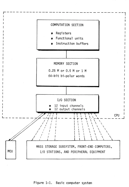
Figure 1-1 represents the basic organization of a CRAY-1 system. The central processor unit (CPU) is a single integrated processing unit consisting of a computation section, a memory section, and an input/ output section. The memory is expandable from 0.25 million 64-bit words to a maximum of 1.0 million words. The 12 input channels and 12
output channels in the input/output section connect to a maintenance control unit (MCU), a mass storage subsystem, and a variety of front-end systems or peripheral equipment. The MCU provides for system initializa-tion and for monitoring system performance. The mass storage subsystem provides secondary storage and consists of one to eleven Cray Research OCU-2 Disk Controllers, each with one to four 00-19 Disk Storage Units. Each 00-19 has a capacity of 2.424 x 109 bits.
I/O channels can be connected to independent processors referred to as front-end computers or I/O stations or can be connected to peripheral equipment according to the requirements of the individual installation. At least one front-end system is considered standard to collect data and present it to the CRAY-1 for processing and to receive output from the CRAY-1 for distribution to slower devices.
r--- - - ---- - --- -- -- - -- --
--~-- - ---- -
--1
,
I
COMPUTATION SECTION
• Registers
• Functional units • Instruction buffers
MEMORY SECTION
0.25 M or 0.5 M or 1 M 64-bit bi-polar words
I/O SECTION
• 12 input channels • 12 output channels
I / I f , t 1 \ \ \ \ ' \ CPU
I I . \ \ \ \ \ ...J
L _ _ _ _ _ _ _ _ _/-1-1
-1- - - -
+ ,... .,... \" " -
~- - - -
--MCU
/ ' 1 I 1 \ \ , \ \ \
#
/'
1 / I / / 1 1 1 \ \ \ \ \ \ 1 \ \ \ \ \ \ / / I i 1 \ \ \ \ \ \/ I 1 \ \ \ \ \ \
/ / I I 1 \ \ \ \ \ \
/1 /1 / : , I, \ \ \ " \\.
MASS STORAGE SUBSYSTEM, FRONT-END COMPUTERS, I/O STATIONS, AND PERIPHERAL EQUIPMENT
[image:21.612.71.521.82.734.2]I
Table 1-1. Characteristics of the CRAY-l Computer System
COMPUTATION SECTION
• 64-bit word
• 12.5 nanosecond clock period • 21
s complement arithmetic
• Scalar and vector processing modes, • Twelve fully segmented functional units • Ei~ht 24-bit address (A) registers
• Sixty-four 24-bit intermediate address (B) registers • Eight 64-bit scalar (5) registers
• Sixty-four 64-bit intermediate scalar (T) registers
• Eight 64-element vector (V) registers, 64-bits per element • Four instruction buffers of 64 16-bit parcels each
• Integer and floating point arithmetic • 128 instruction codes
MEMORY SECTION
• Up to 1,048,576 words of bi-po1ar memory
, (64 data bits and eight error correction bits) • . Eight or sixteen banks
• Four-c1ock-period bank cycle time
• One word per clock period transfer rate toB~ T, and V registers • One word per two clock periods transfer rate to A and S registers • Four words per clock period transfer rate to instruction buffers • Single error correction - double error detection (SEeDED)
INPUT/OUTPUT SECTION
• Twelve input channels and twelve output chann,els
• Channel groups contain either six input or six output channels • Channel groups served equally by memory (scanned every four
clock periods)
• Channel priority resolved within channel groups
,
Sixteen data bits, three control bits per channel, fourparity bits, and an external master clear
[image:22.618.69.540.55.752.2]COMPUTATION SECTION
The computation section contains instruction buffers, reqisters and functional units which operate together to execute a program of instructions stored in memo~y.
Arithmetic operations are either integer or floating point. Inteqer arithmetic is performed in two's complement mode. Floating point quantities have signed-magnitude representation.
The CRAY-1 executes 128 operation codes as either 16-bit (one parcel) or 32-bit (two-parcel) instructions. Operation codes provide for both scalar and vector processing.
Floating point instructions provide for addition, subtraction, multi-plication, and reciprocal approximation. The reciprocal approximation instruction allows for the computation of a floating divide operation using a multiple instruction sequence.
Integer or fixed point operations are provided as follows: integer addition, integer subtraction, and integer multiplication. An integer multiply operation produces a 24-bit result; additions and subtractions produce either 24-bit or 64-bit results. No integer divide instruction is provided and the operation is accomplished through a software
algorithm using floating point hardware.
The instruction set includes Boolean operations for OR, AND, and exclusive OR and for a mask-controlled merqe operation. Shift operations allow the manipulation of either 64-bit or 128-bit operands to produce 64-bit
I
I
MEMORY SECTION
The memory for the CRAY-l normally consists of 16 bank~' of bi-polar LSI memory. Three memory size options are available: 262,144 words, 524,288 words, or 1,048,576 words. Each word is 72 bits long and consists of 64 data bits and 8 check bits. The banks are independent of each other. Sequentially addressed words reside in sequential banks. The memory cycle time is four clock periods (50 nsec). The :access time, that is, the time required to fetch an operand from memory to a scalar register is 11 clock periods (137.5 nsec).
The maximum transfer rate for B, T, and V registers is one word per clock period. For A and S registers, it is one word per two clock periods. Transfers of instructions to the instruction buffers occur at a rate of 16 parcels (four words) per clock period.
Thus, the high speed of memory supports the requirements of scientific applications while its low cycle time is well suited to random access applications. The phased memory banks allow high communication rates through the I/O section and provide low read/store times for vector registers.
INPUT/OUTPUT SECTION
Input and output communication with the CRAY-l is over 12 full duplex 16-bit channels. Associated with each channel are control lines that indicate the presence of data on the channel (ready), data received (resume), or transfer complete (disconnect).
The channels are divided into four channel groups. A channel group consists of either six input paths or six output paths. The four channel groups are scanned sequentially for I/O requests at a rate of
one channel group per clock period. The channel group will be reinterrogated four clock periods later whether any I/O request is pending in the channel or not. If more than one channel of the channel group is active, the requests are resolved on a priority basis. The request from the lowest numbered channel is serviced first.
VECTOR PROCESSING
All operands processed by the CRAY-1 are held in registers prior to their being processed by the functional units and are received by registers after processing. In general, the sequence of operations is to load one or more vector r~gisters from memory and pass them to functional units. Results from this operation are received by another vector register and may be processed additionally in another operation or returned to memory if the results are to be retained.
The contents of a V register are transferred to or from memory by specifying a first word address in memory, an increment for the memory address, and a length. The transfer proceeds beginning with the first element of the V register and incrementing by one in the V register at a rate of up to one word per clock period depending on memory conflicts.
A result may be received by a V register and re-entered as an operand to another vector computation in the same clock period. This mechanism allows for "chaining" two or more vector operations together. Chain operation allows the CRAY-l to produce more than one result per clock period. Chain operation is detected automatically by the CRAY-1 and is not explicitly specified by the programmer, although the programmer may reorder certain code segments in order to enable chain operation.
There may be a conflict between scalar and vector operations only for the floating point operations and storage access. With the exception of these operations, the functional units are always available for scalar operations. A vector operation will occupy the selected functional unit until the
vector has been processed.
Parallel vector operations may be processed in two ways:
1. Using different functional units and all different V registers. 2. Chain mode, using the result stream from one vector register
simultaneously as the operand to another operation using a different functional unit.
operands or one scalar and one vector register as operands. Exceptions are vector shifts, vector reciprocal, and the load or store instructions.
Since many vectors exceed 64 elements, a long vector is processed as one or more 64-element segments and a possible remainder of less than 64
SECTION 2
PHYSICAL ORGANIZATION
INTRODUCTION
The CRAY-1 computer system consists of the following: - The CPU mainframe
- A power cabinet - A condensing unit
- Two motor generators and control cabinets - A maintenance control unit (MCU)
- One or more disk systems, and
- Optional interfaces to one or more front-end comouter systems.
~1AINFRAME
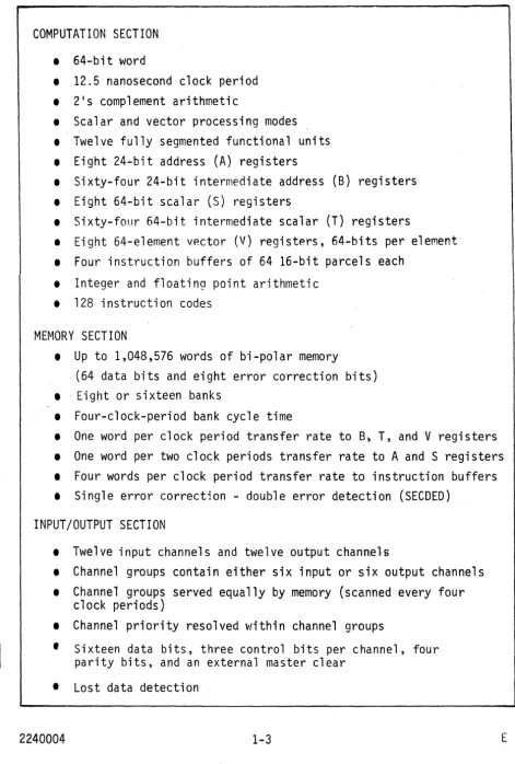
2
The CRAY-1 mainframe, figure 2-1, is composed of 24 logic chassis. The chassis are arranged two per column in a 2700 arc which ;s about five feet in diameter. The twelve columns are about 6 1/2 ft tall. At the base of the col umns, 1 1/2 ft hi gh and extendi ng . outward about 2 1/2 ft, are cabinets for power supplies and cooling distribution systems.
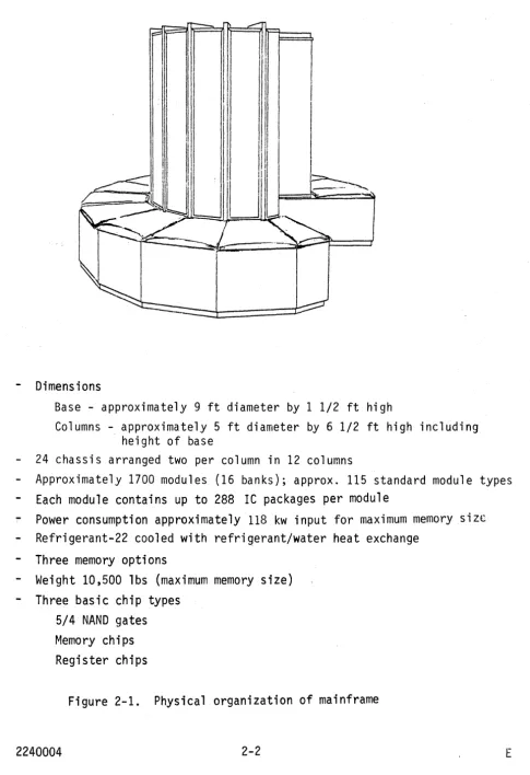
Viewing the cabinet from the top, the chassis of the upper circle are labeled A through L proceeding in a counter-clockwise direction from the opening. The chassis of the lower circle are labeled M through X. The assignment of modules to chassis is illustrated in figure 2-2.
MODULES
I'
IIII1I
I
II
- Dimensions
Base - approximately 9 ft diameter by 1 1/2 ft high
Columns - approximately 5 ft diameter by 6 1/2 ft high including height of base
- 24 chassis arranged two per column in 12 columns
- Approximately 1700 modules (16 banks); approx. 115 standard module types Each module contains up to 288 IC packages per module
Power consumption approximately 118 kw input for maximum memory size - Refrigerant-22 cooled with refrigerant/water heat exchange
- Three memory options
- Weight 10,500 lbs (maximum memory size) - Three basic chip types
5/4 NAND gates Memory chips Register chips
[image:31.618.70.555.43.751.2]1 4 6 48 0 32 24 16 16 24 32 40 48 56 64 71
A B C o
: ~ ! I I ! , STORAGE ! !
CLOCK A:>;[ ADJlRESS FA)/OUT
I
I
I I ; I
!
t-i
- - - - t - - -
---t--I !
Q1EClI B ITS I
I I Q1ECK BITS I
I I
-~r--i
STORAGE
I
CLOCK ANI: ADDRESS FANOUT
M N 0 P
E F
CLK OSC
v pop
CLOCK FANOlrr FLOATING I ~IULTIPLY SCALAR ADD G FLOATING ADD I SCALAR I REGISTERS
SECDED ADDRESS REGISTERS COtITROL
SCALAR
SHIFTS I.OGIC ADDR ADDERS VECTOR
SHIFT
CONTROL NIP I~STR.
CONTROL BUFFERS SECDED VECTOR
ADD XP DATA
H I ! I RECIP. APPROX. SEeDED ADDRESS ~ruLTIPLY
S POP It VECTOR LOGICAL CONTROL SECDED
\'j TO VECTOR I VECTOR SIIIFT STOR.
---r---l-
rVj
'V1
TO ruTO<AC°T ____ _
DATA TO \'ECTOR REGISTERS
I I I
I i I ADDR ___ ~DDR rN0~~ _ _ 1 i FANOUT
i i
I
':0
I
- - - - CLOCKF~~KOUT---
-L -LINE ADPTR
a R 5
L LINE
ADPTR T
Figure 2-2. General chassis layout
J K L
71 64 56 48 40 STORAGE
I I
32 CLOCK ANDI ADDRESS . FANOUT 24
I'
I
16
GlEC1 BITS I Q1ECK BITS
I 16
STORAGE
I I
24
CLOCK AND ADDRESS FANOUT 3 4 4 5 6 71
[image:32.612.88.520.48.738.2]~
There are 1662 modules in a CRAY-1 with a standard 16-bank' memory. Modules are arranged 72 per chassis as illustrated in figure 2-2. There are over 115 module types. Usage varies from 1 to over 700 modules per type. Module type and usage is summarized in Appendix B. Each module type is identified by two letters. The first indicates the module series (A, D, F, G, H, J, M, R, S, T, V, X, and Z). The second letter identifies types of modules within a series.
The computation and I/O modules are on the eight chassis forming the center four columns. Each of the eight chassis on either side of the four center columns contains one of the 16 memory banks.
Modules are cooled by transferring heat via the heat transfer plate to cooling bars which in turn transfer the heat to a refrigerant-22. Power dissipation depends on module density. The average module dissipation by usage is approximately 50 watts.
Two supply voltages are used for each module: -5.2 volts for IC power; -2.0 volts for line termination.
Each module has 96 pin pairs available for interconnecting to other modules. All interconnections are via twisted pair wire. The average utilization of pins is approximately 60 percent.
Each module has 144 available test points that can be used for trouble
shooting. Test points are driven by circuits that do not drive other loads.
CLOCK
All timing within the mainframe cabinet is controlled by a single phase synchronous clock network. This clock has a period of 12.5 nsec. The lines that carry the clock signal from the central clock source to the individual modules of the CPU are all made of uniform length so that the leading edge of a clock signal arrives at all parts of the CPU
I
...
...----12.5 ns---~.[--II~I
____
~~I
~
__ __
~3
ns~
Figure 2-3. Clock pulse waveform
References to clock periods in this manual are often given in the form CPn where n indicates the number of the clock period during which an event occurs. Clock periods are numbered beginning with CPO. Thus, the third clock period would be referred to as CP2.
PO~JER SU PPL I ES
Thirty-six power supplies are used for the CRAY-l computer system. There are twenty -5.2 volt supplies and sixteen -2.0 volt supplies. The supplies are divided into twelve groups of three. Each group supplies one column. The power supply design assumes a constant load. The power supplies do not have internal regulation but depend on the motor-generator to isolate and regulate incoming power. The power supplies use a twelve-phase transformer,
silicon diodes, balancing coil, and a filter choke to supply low ripple DC voltages. The entire supply is mounted on a refrigerant-22 cooled heat sink. Power is distributed via bus bars to the load.
PRIMARY POWER SYSTEM
I
COOLING
Modules in the CRAY-l computer system are cooled by the exchange of heat from the module heat sink to a refrigerant-cooled cold bar. The module heat sink is wedged along both B-inch edges to a cold bar. Cold bars are arranged in vertical columns, with each column having capacity for 144 modules. The cold bar is a cast aluminum bar containing a stainless steel refrigerant tube.
MAINTENANCE CONTROL UNIT
The CRAY-1 computer s¥stem is equipped with a 16-bit minicomputer system that serves as a maintenance tool and provides control for the system initialization. After the CRAY-l operating system has been initialized and is operational, communication with the MCU is via a software protocol. The MCU is connected to a CRAY-l channel pair with additional control signals for execution of the master clear operation, I/O master clear
operation, dead dump operation, and sample parity error operation. The maintenance control unit (MCU) includes:
1. A Data General ECLIPSE minicomputer or equivalent with 32K words of 16-bit memory
2. An BO-column card reader 3. A 132-column 1ine'printer
4. An BOO bpi 9-track tape unit
5. Two display terminals 6. A moving head disk drive
Included in the MCU system is a software packaqe that enables it to serve as a local batch station during production hours. Asa local station, diagnostic routines may be submitted for execution along with other batch jobs. These diagnostics are typically stored on the local
disk and are submitted to the CRAY-l by operator command.
The system initialization procedure is referred to in this manual as the dead start sequence. This sequence is described in detail in Section 3.
FRONT-END COMPUTER
The CRAY-l computer system may be equipped with one or more front-end computer systems that provide input data to the CRAY-l computer system and receive output from the CRAY-l to be distributed to a variety of slow-speed peripheral equipments. A front-end computer system is a self-contained system that executes under the control of its own operating system. Peripheral equipment attached to the front-end computer will vary depending on the use to which the system is put.
A front-end computer may service the CRAY-l in the following ways: • As a local operator station
• As a local batch entry station
• As a data concentrator for multiplexing several other stations into a single CRAY-l channel
• As a remote batch entry station
Detailed information about the front-end system is presented in separate publications.
EXTERNAL INTERFACE
The CRAY-l may be interfaced to front-end systems through special interface controllers that compensate for differences in channel widths, machine word sizes, electrical logic levels, and control protocols. An interface is a Cray Research product and is contained in a small air-cooled stand-alone cabinet located near the front-end computer system. A primary goal of the interface is to maximize the utility of the front-end channel connected to the CRAY-l. Such a channel is generally slower than CRAY-l channels. The CRAY-l may be separ~ted from the interface cabinet by up to 320 ft of cable with no degradation to its effective transfer rate. f1aximum separation of the interface cabinet from the host processor is determined by the channel characteristics of the front-end machine. If site condi-tions require that the interconnected systems be physically located a
MASS STORAGE SUBSYSTEM
Mass storage for the CRAY-1 computer system consists of one or more Cray Research, Inc. OCU-2 Disk Controllers and multiple 00-19 Disk Storage Units. The disk controller is a Cray Research, Inc. product and is implemented in flat-pack ECl logic similar to that used in the CRAY-1 mainframe. The con-troller operates synchronously with the mainframe over a 16-bit full-duplex channel. The controller is in a OCC-1 refrigerant-cooled cabinet located near the mainframe. Up to four controllers may be contained in a cabinet. The cabinet requires about 5 sq. ft. of floor space and is 49 inches high. Each controller may nave from one to four 00-19 disk storage units attached to it. Data passes tnrough the controller to or from one disk storage unit at a time. The controller may be connected to a 16-bit minicomputer station in addition to the CRAY-l. If this additional connection is made, the station and mainframe may share the controller operation. Either, but not both, can have an operation in progress at one time; software interlocks must be provided to avoid conflicts.
Each of the 00-19 disk storage units has two ports for controllers. A second independent data path may exi'st to each disk storage unit through another Cray Research controller. Reservation logic is provided to control access to each disk storage unit.
Operational characteristics of the 00-19 Disk Storage Units are summarized in Table 2-1. Further informati'on about the mass storage subsystem is presented in separate publications.
Ta~le 2-1. Characteristics of a 00-19 Disk Storage Unit
Bit capacity per drive 2.424 x 10⁹ Latency 16.6 msec
Tracks per surface 411 Access time 15 - 80 msec Sectors per track 18 Data transfer rate
Bits per sector 32,768 (average bits per sec.) 35.4 x 10⁶ Number of head groups 10 Total bits that can be streamed to a unit
Recording surfaces (disk cylinder capacity) 5.9 x 10⁶
SECTION 3
COMPUTATION SECTION
INTRODUCTION
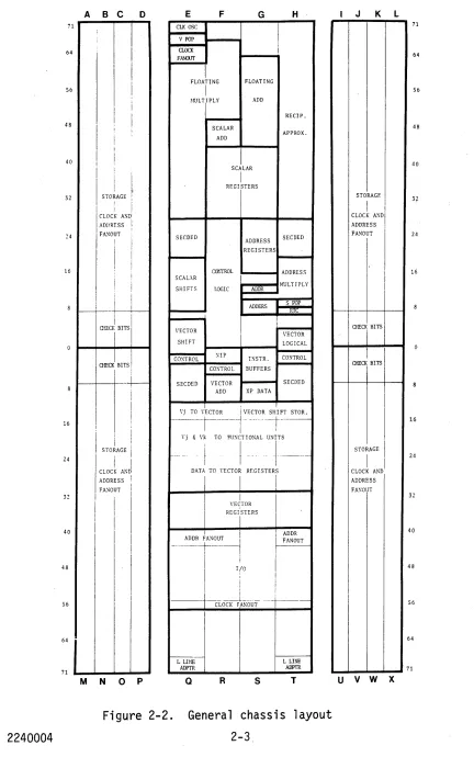
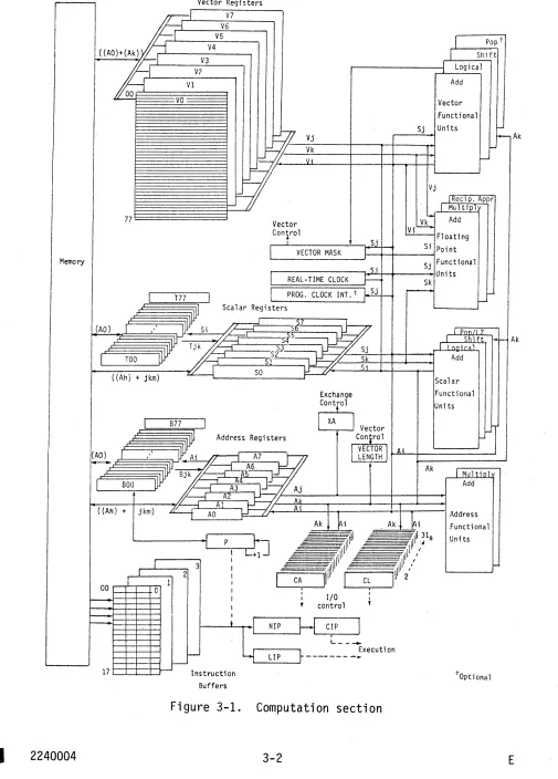
The computation section (figure 3-1) consists of an instruction control network, operating registers, and functional units. The instruction control network performs all decisions related to instruction issue and coordinates the activities for the three types of processing, vector, scalar, and address. Associated with each type of processing are registers and functional units that support the processing mode. For vector processing, there are: a set of 64-bit 64-element registers,
3
three functional units dedicated solely to vector applications, and three floating point functional units supporting both scalar and vector operations. For scalar processing, there are two levels of 64-bit scalar registers and four functional units dedicated solely to scalar processing in addition to the three floating point units shared with the vector operations. For address processing, there are two levels of 24-bit registers and two integer arithmetic functional units.
Vector and scalar processing is performed on data as opposed to address processing which operates on internal control information such as addresses and indexes. The flow of data in the computation section is generally from memory to registers and from registers to functional units. The flow of results is from functional units to registers and from registers to memory or back to functional units. Data flows along either the scalar or vector path depending on the mode of processing it is undergoing. An e~ception is that scalar registers can provide one of the operands required for vector operations performed in the vector functional units.
Vector Registe s r
V7 V6
i V5
I Pop t
((AO)+(Ak) V4 Shift
£
V3 f LogicalI
V?VI Add
VO Vector
Functional Sj Units
r-f- Vj l -Ak
I
= Ij Vk ~
l - I/ Vi t
-~
I-Vj
I-Reclp. Appr
I Multiply
L.
Add
77 Vector
J'1..
Con~rol ~ Floating
i S.i Si
VECTOR MASK r Point
,
Functional
Memory Sj
Si Units REAL- TIME CLOCK ~ Sk
PROG. CLOCK INT. i·pi ~
l-I T77 I
f--
I-IUJ
Scalar Registers
...--J
S57
W
(AO) , I~ 5i ~ f Poo/LZ
"" f Shift
I·t-v~
sf-
¥----'
f I no; rill5j
Add
I TOO ;1- ~ Sk
5 'l" <;i
SO
((Ahj + jkm) Scalar
Ak
Exchange Functional Control Units
I I XA
I
Vector
I B77
rr1
Address Registers Con~rol
( . ;
A~
[ VECTOR
I
Ai(AO) I LENGTH _
-
- ~7i A6 Ak, Mult;Ql
wr
Bjk 7/-;:::1 A5I BOO ~.A _ Add
A3 l__ Aj A2 rj Ak
((Ah) + jkm) ~_ AO Al I/. Ai 1 Address Ak
l
i Ak _ i FunctionalJ =,,11 I~ 318 Units
f P
L+IJ
II :4
,
\11 I' I11\\ I' I
r I I I
3 I
JI
II11
I 1\\\ "
I 2 I
I CA CL I 2
I 1 I
00 i i
0 I I i
I i I/O i
r-- - I t control
,
I
-
-G
H
I-
t NIP crpi
L _ _ _
Execution
f-- LIP ----~
'
-17 Instruction -r Optional
Buffers
[image:41.612.55.560.41.745.2]REGISTER CONVENTIONS
Frequent use is made in this manual of parenthesized register names. This is shorthand notation for the expression lithe contents of register
II For example, "Branch to (P) means "Branch to the address indicated
by the contents of the program parcel counter, P.II
Extensive use is also made of subscripted designations for the A, B, S, T, and V registers. For example, "Transmit (Tjk) to Si" means "Transmit the contents of the T register specified by the jk designators to the S register specified by the i designator. II
In this manual, register bit positions are numbered from left to right starting with bit O. Bit 63 of an S, V, or T register value represents the least significant bit in the operand. Bit 23 of an A or B register value represents the least significant bit in the operand. When a power of two is meant rather than a bit position, it is referred to as 2n, where n is the power of two.
OPERATING REGISTERS
Operating registers are a primary programmable resource of the CRAY-I. They enhance the speed of the system by satisfying the heavy demands for data that are made by the functional units. A single functional unit may require one to three operands per clock period and may deliver results at a rate of one per clock period. Moreover, multiple functional units can be in use concurrently. To meet these requirements, the CRAY-l has five sets of registers; three primary sets and two intermediate sets. The
I
I
V REGISTERS
Eight V registers, each with 64 elements are the major computational registers of the CRAY-I. Each element of a V register has 64 bits.
When associated data is grouped into successive elements of a V register, the register quantity may be considered a vector. Examples of vector quantities are rows or columns of a matrix or elements of a table. Computational efficiency is achieved by processing each element of a vector identically. Vector instructions provide for the iterative processing of successive vector register elements. A vector operation begins by obtaining operands from the first element of one or more V registers and delivering the result to the first element of a V register. Successive elements are provided each clock period and as each operation
is performed, the result is delivered to successive elements of the result V register. The vector operation continues until the number of operations performed by the instruction equals a count specified by the contents of the vector length (VL) register. Vectors having lengths exceeding 64 are handled under program control in groups of 64 and a remainder.
A result may be received by a V register and retransmitted as an operand to a subsequent operation in the same clock period. This use of a register as both a result and operand register allows for the "chaining" of two or more vector operations together. In this mode, two or more results may be produced per clock period.
The contents of a V register are transferred to or from memory in a block mode by specifying a first word address in memory, a positive or negative increment for computing memory addresses, and a vector length. The trans-fer then proceeds beginning with the first element of the V register at a maximum rate of one word per clock period, depending on bank conflicts. Single-word data transfers are possible between an S register and an element of a V register.
In this manual, the V registers are individually referred to by the letter V and a numeric suffix in the range 0 through 7. Vector instructions reference V registers by allowing specification of the suffix as the i, j,
I
Individual elements of a V register are designated in this manual by deci-mal numbers in the range 00 through 63. These appear as subscripts to vector register references. For example, V629 refers to element 29 of vector register 6.
V register reservations
The term "reservation" describes the register condition when a register is in use and therefore not available for use as a result or as an operand register for another operation. During execution of a vector instruction, reservations are placed on the operand V registers and on the result V register. These reservations are placed on the registers themselves, not on individual elements of the V register.
A reservation for a result register is lifted during "chain slot". time. Chain slot time is the clock period that occurs at functional unit time plus two clock periods. During this clock period, the result is
available for use as an operand in another vector operation. Chain slot time has no effect on the reservation placed on operand V registers. A V register may serve only one vector operation as the source of one or both operands.
No reservation is placed on the VL register during vector processing. If a vector instruction employs an S register, no reservation is placed on the S register. It may be modified in the next instruction after vector issue without affecting the vector operation. The length and scalar operand (if appropriate) of each vector operation is maintained apart from the VL register. Vector operations employing different lengths may proceed con-currently; however, the vector length should not be changed between opera-tions that chain because chaining implies operaopera-tions of the same length. The Ao and Ak registers in a vector memory reference are treated in a
VECTOR CONTROL REGISTERS
Two registers are associated with vector registers and provide control information needed in the performance of vector operations. They are the vector length (VL) register and the vector mask (VM) register. -VL register
The 7-bit vector length register can be set to 0 through 100s and specifies the length of all vector operations performed by vector instructions and the length of the vectors held by the V registers. It controls the number of operations performed for instructions 140 through 177. The VL register may be set to an A register value through use of the 0020 instruction.
Cray Research cautions users against changing VL between operations that may chain together. In code sequences where the vector length is increased, unexpected results may occur.
Suppose, for example, that during a vector sequence the contents of VL are changed to a larger value and a second operation is initiated to chain to the first operation. The user may expect that the second operation will use the results of the first operation and the operands in the register unaltered by the first operation. However, when the instructions chain together, the second instruction does not receive the anticipated operands beyond the VL specified for the first operation. The user who intends to use the system in this manner must take care to avoid chained operations. Although there may be applications of the characteristic produced by chained operations with different contents for VL, Cray Research takes no responsibility for its use. Chained operation cannot be assured since I/O interrupts may IIbreak" the chain.
VM register
The vector mask register has 64 bits, each of which corresponds to a word element in a vector register. Bit 0 corresponds to element 0, bit 63 to element 63. The mask is used in conjunction with vector merge and test instructions to allow operations to be performed on individual vector elements.
S· REGISTERS
The eight 64-bit S registers are the principal scalar registers for the CPU. These registers serve as the source and destination for operands in the execution of scalar arithmetic and logical instructions. The related functional units perform both integer and floating point arith-metic operations.
S registers may furnish one operand in vector instructions. Single-word transmissions of data between an S register and an element of a V register are also possible.
Data can move directly between memory and S reqisters or can be placed in T registers as an intermediate step. This allows buffering of scalar operands between S registers and memory.
Data can also be transferred between A and S registers.
Another use of the S registers is for setting or reading the vector mask
,(VM) register or the real-time clock register.
At most, one S register can be entered with data during each clock period. Issue of an instruction is delayed if it would cause data to arrive at the S registers at the same time as data already being processed which is scheduled to arrive from another source.
When an instruction issues that will deliver new data to an S register, a reservation is set for that register to prevent issue of instructions that read the register until the new data has been delivered.
In this manual, the S registers are individually referred to by the letter S and a numeric subscript in the range 0 through 7. Instructions reference S registers by allowing specification of the subscript as the i, j, or k
designator as described in section 4 of this manual. The only register to which an implicit reference is made is the So register. The use of this register is implied in the following branch instructions:
014 through 017.
T REGISTERS
There are sixty-four 64-bit T registers in the computation section. The T registers are used as intermediate storage for the S registers.
Data may be transferred bidirectionally between T and S registers and between T registers and memory. The transfer of a value between a T register and an S register requires only one clock period. T registers reference memory through block read and block write in~tructions. Block transfers occur at a maximum rate of one word per clock period. No
reservations are made for T registers and no instructions can issue during block transfers to and from T registers.
In this manual, T registers are referred to by the letterT and a 2-digit octal subscript in the range 00 through 77·. Instructions reference T registers by allowing specification of the octal subscript as the jk designator as described in section 4 of this manual.
A REGISTERS
The eight 24-bit A registers serve a variety of applications. They are primarily used as address registers for memory references and as index registers but also are used to provide values for shift counts, loop control, and channel I/O operations. In address applications, they are used to index the base address for scalar memory references and for providing both a base address and an index address for vector memory references.
The address functional units support address and index generation by
performing 24-bit integer arithmetic on operands obtained from A registers and delivering the results to A registers.
Data can move directly between memory and A registers or can be placed in B registers as an intermediate step. This allows buffering of the data between A registers and memory.
Data can also be transferred between A and S registers.
At most, one A register can be entered with data during each clock period. Issue of an instruction is delayed if it would cause data to arrive at the A registers at the same time as data already being processed which is scheduled to arrive from another source.
When an instruction issues that will deliver new data to an A register, a reservation is set for that register to prevent issue of instructions that read the register until the new data has been delivered.
In this manual, the A registers are individually referred to by the letter A and a numeric subscript in the range 0 through 7. Instructions reference A registers by allowing specification of the subscript as the h, i, j, or k designator as described in section 4 of this manual. The only register to which an implicit reference is made is the Ao register. The use of this register is implied in the following instructions:
010 through 013 034 through 037 176 and 177
Refer to section 4 for additional information concerning the use of A registers by instructions.
B REGISTERS
There are sixty-four 24-bit B registers in the computation section. The B registers are used as intermediate storage for the A registers. Typically, the B registers will contain data to be referenced repeatedly over a
sufficiently long span that it would not be desirable to retain the data in either A registers or in memory. Examples of uses are loop counts, variable array base addresses, and dimensions.
In this manual, B registers are individually referred to by the letter B and a 2-digit octal subscript in the range 00 through 77. Instructions reference B registers by allowing specification of the octal subscript as the jk designator as described in section 4 of this manual. The only B
register to which an implicit reference is made is the Boo register. On execution of the return jump instruction (007), register Boo is set to the next instruction parcel address and a branch to an address specified by ijkm occurs. Upon receiving control, the called routine will con-ventionally save (Boo) so that the Boo register will be free for the
called routine to initiate return jumps of its own. When a called routine wishes to return to its caller, it restores the saved address and executes a 005 instruction. This instruction, which is a branch to (Bjk),.causes the address saved in Bjk to be entered into P as the address of the next instruction parcel to be executed.
FUNCTIONAL UNITS
Instructions other than simple transmits or control operations are
performed by hardware organizations known as functional units. Each unit implements an algorithm or a portion of the instruction set. Units are independent; a number of functional units can be in operation at the same time.
A functional unit receives operands from registers and delivers the result to a register when the function has been performed. The units operate essentially in three-address mode with source and destination addressing limited to register designators.
All functional units perform their algorithms in a fixed amount of time; no delays are possible once the operands have been delivered to the unit. The amount of time required from delivery of the operands to the unit to the completion of the calculation is termed the "functional unit time" and is measured in 12.5 nsec clock periods.
I
clock period even though the functional unit time may be more than one clock period. This segmentation is made possible by capturing and holding the information arriving at the unit or moving within the unit at the end of every clock period.
Twelve functional units are identified in this manual and are arbitrarily described in four groups: address, scalar, vector, and floating point. The first three groups each act in conjunction with one of the three primary register types, A, S, and V, to support the address, scalar, and vector modes of processing available in the CRAY-l. The fourth group, floating point, can support either scalar or vector operations and will accept operands from or deliver results to S or V registers accordingly.
ADDRESS FUNCTIONAL UNITS
The address functional units perform 24-bit integer arithmetic on operands obtained from A registers and deliver the results to an A register. The arithmetic is two1s complement.
Address add unit
The address add unit performs 24-bit integer addition and subtraction.· The unit executes instructions 030 and 031. The addition and subtraction are performed in a similar manner. However, the two1s complement subtraction for the 031 instruction occurs as follows. The one's complement of the Ak operand is added to the Aj operand. Then a one is added in the low order bit position of the result.
No overflow is detected in the functional unit. The functional unit time is two clock periods. Address multiply unit
The address multiply unit executes instruction 032, which forms a 24-bit integer product from two 24-bit operands. No rounding is performed. The result consists of the 24 least significant bits of the product.
SCALAR FUNCTIONAL UNITS
The scalar functional units perform operations on 64-bit operands obtained from S registers and in most cases deliver the 64-bit results to an S register. The exception is the population/leading zero count unit which delivers its 7-bit result to an A register.
Four functional units are exclusively associated with scalar operations and are described here. Three functional units are used for both scalar and vector operations and are described under the section entitled
Floating Point Functional Units. Scalar add unit
The scalar add unit performs 64-bit integer addition and subtraction. It implements instructions 060 and 061. The addition and sUbtraction are per-formed in a similar manner. However, the two's complement subtraction for the 061 instruction occurs as follows. The one's complement of the Sk operand is added to the Sj operand. Then a one is added in the low order bit position of the result.
No overflow is detected in the unit.
The functional unit time is three clock periods. Scalar shift unit
The scalar shift unit shifts the entire 64-bit contents of an S register or shifts the double 128-bit contents of two concatenated S registers. Shift counts are obtained from an A register or from the jk portion of the instruction. Shifts are end off with zero fill. For a double shift,
a circular shift is effected if the shift count does not exceed 64 and the i and j designators are equal and non-zero.
Scalar lo~ical unit
The scalar logical unit performs bit-by-bit manipulation of 64-bit quantities obtained from S registers. It implements instructions 042 through 051, the mask and Boolean instructions. An operation requires only one clock period.
Population/leading zero count unit
This functional unit implements instructions 026 and 027. The 026
instruction, which counts the number of bits having a value of one in the operand, executes in four clock periods. The 027 instruction, which counts the number of bits of zero preceding a one bit in the operand, executes in three clock periods. For either instruction, the 64-bit operand is obtained from an S register and the 7-bit result is delivered
to an A register.
When the Vector Population Instructions Option is installed, this unit also recognizes an additional instruction, the 026ijl instruction, which
returns a one-bit population count parity (even) of an S register's contents to an A register.
VECTOR FUNCTIONAL UNITS
Most vector functional units perform operations on operands obtained from one or two V registers or from a V register and an S register. The
reciprocal unit, which requires only one operand, is an exception. Results from a vector functional unit are delivered to a V register.