Read/Write Stability Improvement of 8T Sram Cell
Using Schmitt Trigger
Dr. A. Senthil Kumar
*,I.Manju
**, S.Sumathi
**, C.Preethi
*** *Professor , Electrical and Electronics Engineering, Velammal Engineering College **
Assistant Professor, Electronics and Communication Engineering, Velammal Engineering College ***
Student, Electronics and Communication Engineering, Velammal Engineering College
Abstract- In recent years the demand for low power devices has increased tremendously due to the migration of computer workstations to handheld devices that need real-time performance within the budget for physical size and energy dissipation. As a result of this there is a fast growth of battery operated portable applications such as PDAs, cell phones, laptops and other handheld devices. But also at the same time problems arising from continuous technology scaling have recently made power reduction an important design issue for the digital circuits and applications. Operating at low power causes SRAM read-stability and write- ability as major design constraints. The stability of read and write operations can be increased using Schmitt trigger based SRAM bit cells. In this paper the Schmitt trigger design is implemented in 8 transistor SRAM cell to increase read-stability and write-ability than the conventional 6T cell. The design is implemented in Tanner EDA tool and the results are observed.
Index Terms- low power usage, 6T cell, stability.
I. INTRODUCTION
he growing market of portable battery-operated systems demands micro-electronic circuit design with ultra low power dissipation. This emerging portable SoC designs demand for low power SRAMs. The overall power dissipation can be achieved through the scaling down of supply voltage [1]. But reducing the supply voltage limits the circuit to operate in low power due to effect of process variations. It is forecasted that embedded memory in SOC designs will cover up to 90% of the total chip area. To achieve longer battery life in portable devices low-power SRAM array is necessary. Due to technology scaling, the number of transistors on a die is increased causing a increase in density. This has an exponential impact on leakage power. The Schmitt trigger design reduces the leakage current thereby reducing power consumption.
In section II, the conventional 6T SRAM design is discussed, its operation and drawbacks. In section III, available 6T ST design is discussed. In section IV the proposed 8T design is discussed. In section V the design and output waveform for the existing 6T cell and the proposed design are given.
II. PRELIMINARY STUDIES
Depending upon various design goals such as bit density, bitcell area, low voltage operation several SRAM cells have been
proposed. A 6T bit cell is the most commonly used memory bitcell in the present designs[1]. Full Transmission gates are used in a Single-ended 6T bit cell[9]. In this design write ability is achieved by modulating the virtual-vcc and virtual vss. Single ended 7T bit cell[2] consists of a single ended write operation and a separate read port.S . Birla et al in their work[11], found that as voltage decreases the SNM decreases in a 8T cell which along with a leakage reduction mechanism will provide a better stability.
A low power read stable single-ended 8T cell designed[12] and it is shown that it consumes less power than the conventional 6T cell. It is shown in [13],[14] that stacking of transistors will reduce the leakage. A differential 10T bit cell with two separate ports are also reported.
From the study, it is clear that the basic element for storage is a cross-coupled inverter pair. For a successful operation of SRAM cell with better read and write stability a new design approach is required. Hence, Schmitt trigger based design is implemented in 8T cell to achieve the above mentioned stability.
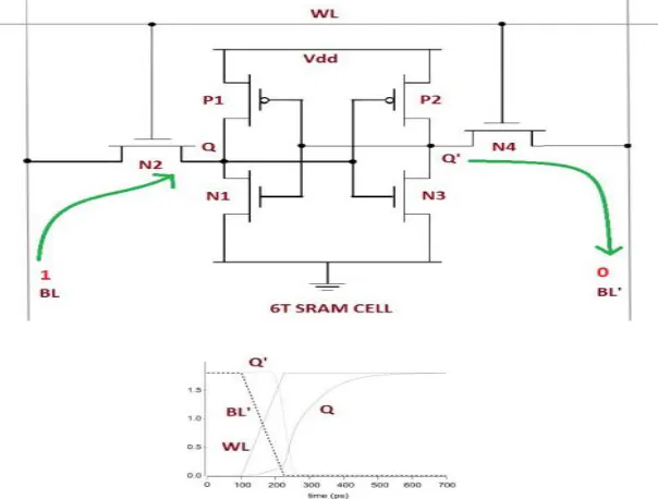
III. AVAILABLE 6T CELL AND ITS DRAWBACK The mainstream six-transistor (6T) CMOS SRAM cell is shown in the figure. The SRAM cell constituted of a flip-flop. The logical values ‘0’ or ‘1’ get stored at the storage nodes[8]. This 6T cell consists of two inverters: Load MOSFET and Driver MOSFET and two access MOSFETs that are connected to bit lines (BL & BL’). The access transistors are also connected to a word line (WL). To form a flip-flop, the input and output of one inverter is connected to the output and input of another inverter, respectively. This forms a cross-coupled pair of inverters.
Read operation
Bit lines are precharged to supply voltage before read operation. The read operation is initiated by enabling the word line (WL) and thereby connecting the internal nodes of the SRAM bitcell to bit-lines. The bit line voltage is pulled down by the NMOS transistor at the ‘0’ storage node and the difference between two bit line voltages will be detected by sense amplifier. When the word line (WL) is high, one of the bit line voltages is pulled down through transistors M2 and M6 or M1 and M4. The transistors M2 and M6 forms a voltage divider, because of current flowing through M2, the potential at node is no longer at ‘0’v. Also it should not go beyond switching threshold inverter (INV1) to avoid destructive read. The rising of potential depends on sizing of access transistor and pull down transistor which is
defined as a bit cell ratio. The read operation is explained with a diagram which is given below,
Figure 1 Read Operation of 6T cell
Write operation
During write operation, the pre-charged logic is kept at low. Suppose to store logic ‘1’. Bit line is charged to and bit bar line is discharged to ground. When the word line is activated, the data
[image:2.612.162.464.370.599.2]on bit and bit bar lines are written into the output nodes of the cell. During updating of content, one should remember that the voltage where logic ‘1’ is stored must be less than the threshold voltage of the driver transistor of other inverter.
Figure 2 Write operation of conventional 6T cell
Drawback of 6T SRAM cell
The conventional 6T cell schematic shown in the above figure is the most commonly used SRAM implementation and it has the advantage of very less area. However, the potential stability problems of this design arises during read and write operation, where the cell is most vulnerable towards noise and thus the stability of the cell is affected. If the cell structure is not designed properly, it may change its state during read and write operation.
power. So to improve the inverter characteristics, Schmitt trigger configuration is used.
Figure 3 Schmitt Trigger configuration
To resolve the conflict present between the read and write design requirements in the conventional 6T bit cell, we need to apply Schmitt Trigger(ST) principle for the cross-coupled inverter pair. The feedback mechanism is used in the pull-down path in this STSRAM bit cells. By raising the source voltage of pull-down NMOS (N1), the feedback transistor tries to preserve the logic ‘1’ while the input transition is made as 0. This results in higher switching threshold of the inverter with very sharp transfer characteristics. Since read-failure is initiated by a 0 input transition for the inverter storing logic ‘1’, higher switching threshold with sharp transfer characteristics of the Schmitt trigger gives robust read operation. During the transition the feedback mechanism is not present.
This results in smooth transfer characteristics that are essential for easy write operation. Thus input dependent transfer characteristics of the Schmitt trigger improves both read stability as well as write-ability of the SRAM bit cell.
The above achieved stability can further be increased by introducing read/write assist techniques along with the Schmitt trigger design. By introducing more transistors the read and write operation can be designed not to affect the stored value.
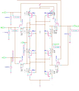
V. PROPOSED 8T SCHMITT TRIGGER CELL In a eight-transistor (8T) CMOS SRAM cell, extra transistors are added to the conventional 6T cell, so that the read and write operation are seperated. This topology was originally
[image:3.612.322.578.100.398.2]proposed for a sub-threshold SRAM design. It is optimized to operate at low power. The proposed design is given below in the figure.
Figure 4 Proposed 8T ST SRAM cell
VI. RESULTS AND DISCUSSIONS
Figure 5 Schematic of 6T ST in Tanner Tool
[image:4.612.176.436.391.634.2]Figure 7. Schematic of 8T ST SRAM cell in Tanner Tool
Figure 9 Waveform for the operation of 8T ST cell in tanner
VII. CONCLUSION
Supply voltage reduction is the effective way for ultra low power operation. Thus in this paper, a stable SRAM cell design is implemented through the use of Schmitt trigger based SRAM design in the eight transistor cell.
REFERENCES
[1] Jaydeep .P. kulkarni, Kaushik Roy, “Ultra low voltage process variation tolerant Schmitt trigger based design”, IEEE transactions on very large scale integration, vol. 20, February 2012.
[2] T. Suzuki, H. Yamauchi, Y. Yamagami, K. Satomi, and H. Akamatsu, “A stable 2-port SRAM cell design against simultaneously read/write disturbed access”, IEEE J.Solid state circuits,vol 43,no. 9,Sep 2008.
[image:5.612.132.375.367.587.2][4] Z. Liu and V. Kursun, “High read stability and low leakage cache memory cell,” IEEE Trans. Very Large Scale Integr (VLSI) syst,vol.16,no.4,Apr 2008.
[5] A. Bhavnagarwala, X. Tang and J. Meindl, “The impact of intrinsic device fluctuations on CMOS SRAM cell stability”,IEEE J.Solid State Circuits, Vol,36,no,4,Apr 2001.
[6] K. Roy and S. Prasad, “Low Power CMOS VLSI Circuit Design, 1st ed. New York:Wiley 2000.
[7] J. P. Kulkarni, K. Kim and K. Roy, “A 160 mV robust Schmitt trigger based subthreshold SRAM,” IEEE J.Solid-State Circuits, vol.42,no.10,Oct.2007. [8] Koichiro Ishibashi, Kenichi Osada ,Low power and reliable SRAM memory
array, Springer.
[9] B. Zhai, D. Blaauw, D. Sylvester, and S.Hanson, “ A sub-200mV 6T SRAM in 0.13µm CMOS,” in proc. Solid State circuits conf, Feb 2007. [10] H. Mahmoodi, S. Mukhopadhyay and K. Roy, “Modeling of failure
probability and statistical design of SRAM array for yield enhancement in nanoscaled CMOS,” IEEE Trans. COmput-Aided Design(CAD),Dec 2005. [11] S. Birla ,Neeraj Kumar, Kapil , “Analysis of 8T SRAM cell at Various
Process Corners at 65nm process technology,” Scientific research,Circuita and systems,2011.
[12] Nahid Rahman, B. P. Singh, “ Design of low power SRAM memory using 8T SRAM cell, International Journal of Recent Technology and Engineering, vol.2, March 2013.
[13] S. Lin, Y.B. Kim and F. Lombardi, “ A highly-stable nanometer memory for low-power design,”in proc.IEEE Workshop design test of Nano devices, Circuits 2008
[14] S. Verkila, S. Bondada, and B.Amrutur, “A 100MHz to 1 GHz,0.35V to 1.5V supply 256 x 64 SRAM block using symmetrized 9T SRAM cell with controlled read,” in proc .Int.Conf.VLSI Design,2008
AUTHORS
First Author – Dr. A. Senthil Kumar, Professor , Electrical and
Electronics Engineering, Velammal Engineering College, Chennai, India, [email protected]
Second Author – I.Manju, Assistant Professor, Electronics and
Communication Engineering, Velammal Engineering College, Chennai, India, [email protected]
Third Author – S.Sumathi, Assistant Professor, Electronics and
Communication Engineering, Velammal Engineering College, Chennai, India, [email protected]
Fourth Author – C.Preethi, Student, Electronics and