High Throughput LFSR Design for BCH Encoder using
Sample Period Reduction Technique for MLC NAND
based Flash Memories
Manikandan.S.K
Assistant Professor (Sr.Gr.), Department of EEE,
Velalar College of Engineering and Technology Erode, Tamilnadu
Nisha Angeline. M
Assistant Professor (Sr.Gr.), Department of ECE,
Velalar College of Engineering and Technology Erode, Tamilnadu
Sharmitha.E.K
PG Student, Department of ECE,
Velalar College of Engineering and Technology Erode, Tamilnadu
Palanisamy.C
Professor and Head, Department of IT,
Bannari Amman College of Technology, Sathyamangalam, Tamilnadu
ABSTRACT
Error correction is one of the important technique for detecting and correcting errors in communication channels, memories etc., Errors are associated with all types of memories. But the NAND FLASH memories are competing in the market due to its low power, high density, cost effectiveness and design scalability. As far as the memory is concerned the testing should not consume more time. So, some DSP algorithms are used to overcome the delays by increasing the sampling rate. BCH codes are widely been used for error detection and correction. The generated check bits of the BCH encoder are appended with the message bits to form a codeword. This codeword is sent to the receiver to detect any error during the transmission. One of the main components of BCH encoder is LFSR (Linear Feedback Shift Register). LFSR find its wider application in Built-in-Self-Test, signature analyzer etc., whereas here it is used to form parity bits to concatenate with message bits for the formation of a codeword. The main advantage of LFSR is that it is simple to construct and it operates at very high clock speed, but its main drawback is that the inputs are given in bit serial. To overcome these drawbacks, DSP algorithms such as unfolding and parallel processing are used by selecting the unfolding factor based on some design criteria. Selecting a better unfolding value reduces the sample period, decreases the clock cycle, and increases the speed, power and the throughput.
KEYWORDS
Bose Chaudhuri-Hocquengham (BCH), Cyclic Redundancy Check (CRC), Computational Time (CT), Galois Field (GF), LFSR, MLC (Multi Level Cell), unfolding, sample period reduction.
1.
INTRODUCTION
NAND Flash's high-density, low power, cost effective, and scalable design make it an ideal choice to fuel the explosion of new multimedia products that are entering the market. Advances in system design techniques also enable the
more cost effective NAND Flash to replace NOR Flash in a significant percentage of traditionally NOR Flash applications. NAND flash performs read and write simultaneously. Due to the efficient architecture of the NAND Flash, its cell size is almost half the size of a NOR cell. This enable NAND Flash architecture to offer higher densities with larger capacity on a given die size, in combination with a simpler production process [1].
This paper focus on NAND Flash memories since they have lower erase times, less chip area per cell which allows greater storage density, and lower cost per bit than NOR Flash memories. NAND is used or best suited for sequential data application. Physically, the NAND architecture uses smaller transistors, because it doesn't have to “pull-down” a whole bit-line. A NAND bit line is a series of transistors so each transistor only has to pass a small amount of current.
There are some inherent limitations of NAND Flash memories [2]. These include write/read disturbs, data retention errors, bad block accumulation, limited number of writes, program disturb errors, soft errors and stress-induced leakage current. Because of these errors that occur in MLC NAND based flash memories various types of coding techniques can be applied for error detection and correction.
unfolding concept. Parallel processing increases the number of message bits to be processed in a clock cycle (sample rate), but increases the area also.
Unfolding is a transformation technique, which describes J consecutive iterations of the original DSP program. Unfolding increases the Iteration bound to J . In order to reduce the sampling period it is important to calculate the iteration bound before unfolding the system to select the unfolding factor. Many important cases such as CT > and is not an integer must be analyzed before selecting the unfolding factor. The selected unfolding value must make CT and is an integer, which automatically reduces the sampling period. Unfolding is a transformation technique that can be applied to any DSP program to create a new program, which describes more than one iteration of the original program [5]. Large number of iterations of an original program can be made by unfolding it by an unfolding factor.
The rest of the paper is organized as follows. Section II gives the brief summary of the Existing System. Section III contains the design procedure of LFSR for BCH (31, 16) and criteria for selecting the unfolding factor to propose a new unfolded structure to reduce the sample period and gives the steps for unfolding the DFG of the LFSR. Section IV contains the algorithm for unfolding and proposed a new architecture for LFSR. Section V analyses the data flow, area and clock cycle of LFSR for different unfolding
2. EXISTING SYSTEM
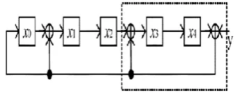
[image:2.595.339.524.80.158.2]There are various recursive formulas developed in past to achieve the parallel architecture for CRC hardware [6]. High-speed architectures for parallel long BCH encoders are developed in [7] for a particular generator polynomial of lower order. However, the unfolding factor is not selected by analyzing various cases. Resource Sharing and power optimization techniques are applied in [6] to achieve low power high-throughput BCH error correction in VLSI for multi-level cell NAND flash memories. Novel look ahead techniques are used to improve the throughput for the generator polynomial of lower order [8] without considering the important criteria for selecting the unfolding factor. Retiming and unfolding of CRC architectures are introduced for lower order generator polynomial to increase the speed [9] without selecting the unfolding factor by considering some important criteria. The normal architecture and the unfolded architecture [5] are shown in Figure 1 and 2.
[image:2.595.84.255.590.657.2]Figure 1: CRC architecture for g(x) = 1+ y+
Figure 2: Two-Parallel CRC architecture for g(x) = 1+
y+ for J = 2
3. PROPOSED SYSTEM
The basic architecture of the proposed system is unfolded LFSR, for generating the parity bit. Compare to normal LFSR, the proposed unfolded LFSR architecture uses sample period reduction technique to achieve more speed. In order to achieve this objective, some important criteria has to be considered for selecting the unfolding factor to improve the design methodology. Data flow table for the proposed system and conventional system is tabulated and compared in Table 1,2 and 3. Then, area and power analysis of the proposed and conventional LFSR is graphically shown in Figure 7,8 and 9 to analyze the depth on the hardware and power overhead. Different levels of unfolding factors are introduced to check the hardware complexity and speed of the design.
3.1
Design of LFSR for BCH (31,16)
BCH codes are subset of the Block codes. BCH codes belong to a powerful class of multiple error correcting codes [10]. BCH codes are based on well-defined mathematical properties. These mathematical properties are based on the Galois Field or finite fields [3]. The Finite field has the property that any arithmetic operations on field elements always have results in the field only [3]. To provide an excellent error correcting capability, the roots of the generator polynomial of the BCH codes have to be specified carefully. With a generator polynomial of g(x), a t- error correcting cyclic codes is the binary BCH codes, with a condition that g(x) must be the least degree polynomial over Galois Field GF(2). Steps for designing the generator polynomial of BCH (31,16) is explained below,
i) Choose an irreducible polynomial p(x) = ii) Construct GF ( )
iii) Construct the minimal polynomial using the
relation (X)= ) (1)
α: = m1(x)
= m2(x)
= m3(x)
where β be a non-zero element of GF( ).
iv). Form the generator polynomial using the relation g(x)=LCM(m1(x),m2(x),m3(x)). (2)
In this proposed work, BCH (31, 16) is taken as an example and an encoder is designed for it using the generator polynomial,
g(x)= +1
Hence, the resultant message bit is 22 bit long, which is divided by the generator polynomial to form parity bits.
The parity bits that are obtained from LFSR is 100101000100010. This is systematic encoding, because information and check bits are arranged together so that they can be recognized in the resulting codeword.
General equation for codeword is,
i(x). =q(x).g(x) +r(x) (3)
Where,
i (x):information bit polynomial. q (x):quotient bit polynomial. g (x):generator polynomial. r (x):remainder polynomial.
[image:3.595.55.570.192.421.2]Encoder of BCH(31,16) comprises of parallel in serial out shift register followed by the LFSR.
Figure 3: LFSR Architecture for g(x) = +1
3.2
Unfolding LFSR
Unfolding algorithm is applied only to the LFSR architecture in this proposed design to increase the speed by reducing the sampling period.
The steps to be followed to unfold the encoder are,
i) Convert normal LFSR into DFG ii) Calculate the iteration bound for the DFG
iii) If < CT of a node, apply unfolding to make the sampling period to be equal to . This technique is called as sample period reduction.
3.2.1
Formation of DFG for the LFSR
Often a DSP program is represented using the DFG. Here the nodes represent the computation and each of the node has its own computation time. The communication between the nodes is represented using edges. The DFG for the LFSR is shown in Figure 4.
[image:3.595.105.490.572.733.2]3.2.2 Calculation Of Iteration Bound
Many of the DSP algorithms contain feedback loops, which impose an inherent fundamental lower bound on the achievable iteration or sample period. This bound is referred to as iteration bound. Iteration bound is the representation of the algorithm in the form of a DFG. Same algorithm but with different representations lead to different iteration bound. Iteration bound is defined as,
= (4)
Iteration bound is the maximum of loop bound
= }
= = .
3.2.3
Sample Period Reduction
The loop 10 ⟶ 9 ⟶ 8⟶ 7 ⟶ 6 ⟶ 5 ⟶ 4 ⟶ 3 ⟶ 2 ⟶ 1 has the maximum loop bound. Synthesis report reveals that all the nodes of the DFG has CT of 1u.t. Since < CT, iteration period cannot be made equal to . In such a case retiming can be applied but it cannot be used to reduce the CT of the critical path of the DFG to . Selection of the unfolding factor is an important criterion in sample period reduction. Unfolding factor is chosen using the relation, J=┌ ┐= 2. Iteration bound of the unfolded DFG changes from . Where J stands for the unfolding factor. Similarly the sample period of the unfolded DFG is . One more case exist is, if is not an integer. The LFSR of g(x)
= +1
satisfies both the cases. Because its CT is greater than the iteration bound and the iteration bound is not an integer. Hence J must be selected in such a way that is an integer and > node CT. The only value of J that satisfies both the condition is 3. This is clearly specified by a theorem [5].
4. UNFOLDING ALGORITHM
It is a transformation technique that can be applied to a DSP program in order to create a new program describing more than one iteration of the original program. Unfolding a DSP program is done by selecting an unfolding factor J, which describes J consecutive iterations of the original program. Loop unrolling is also called as unfolding [5].
4.1
Algorithm Steps
1. For each node U in the original DFG, draw J nodes
2. For each edge U ⟶ V with w delays in the original DFG, draw the J edges with└ ┘ delays for i = 0,1,……J-1. (5)
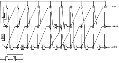
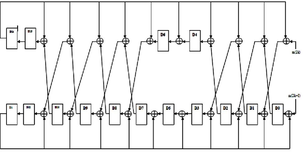
[image:4.595.57.543.428.688.2]By this technique the speed of the LFSR is increased automatically by reducing the clock cycle. The main drawback of unfolding is that the area of the system increases and choosing a large value of unfolding factor leads to hardware complexity. After applying the unfolding technique with unfolding factor J=3 and 2 for Figure 3, three parallel and two parallel architectures are obtained and it is shown in Figure 5 and 6.
Figure 6: Three parallel LFSR for g(x) = +1 after Unfolding by a factor of 2
After the application of unfolding, the sample period is reduced and the iteration bound is increased from 0.66 to 1.32. So that J > CT. This sample period reduction is one of the application of the unfolding algorithm.
5. RESULTS AND ANALYSIS
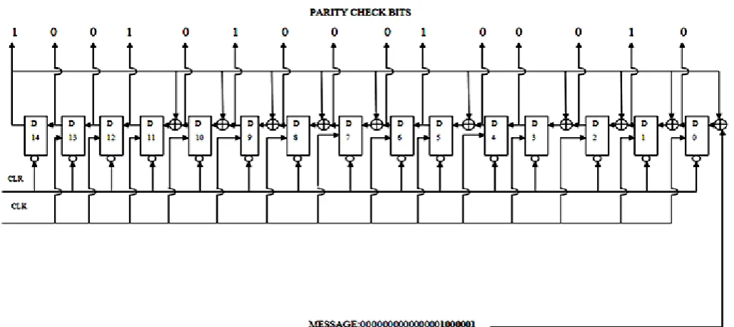
Initially the codeword is formed by the generation of parity bits 100100010100010. This parity bit formation is coded in VHDL. Each of the unfolded architecture is coded in VHDL, simulated and implemented using Xilinx92i to analyze the area and speed. For the message bits: 0000000001000001 and for the generator polynomial g(x)
= +1 the
normal BCH encoder simulation result is shown in Figure 10. The same architecture but with unfolding factor of 2 and 3 is simulated and verified as shown in Figure 11 and 12. From the results shown in Table 1, 2, 3 and 4, it is clear that the clock cycle decreases from 22 to 8 because of sample period reduction technique. Hence unfolding speed up the LFSR operation by decreasing the clock cycle. As far the memory is concerned, the error detection and correction must not take much time because it decreases the throughput of the system.
[image:5.595.346.543.576.726.2]5.1
Data Flow Table
Table 1: Data flow table for normal LFSR
Clock Message bit y(14 to 0)
1 2 3 4 5 6 7 8
1 0 0 0 0 0 1 0
000000000000001 000000000000010 000000000000100 000000000001000 000000000010000 000000000100000 000000001000001 000000010000010
9 10 11 12 13 14 15 16 17 18 19 20 21 22
0 0 0 0 0 0 0 0 0 0 0 0 0 0
000000100000100 000001000001000 000010000010000 000100000100000 001000001000000 010000010000000 100000100000000 000110110101111 001101101011110 011011010111100 110110101111000 101010101011111 010010100010001 100101000100010
Table 2. Data flow table for LFSR with unfolding factor of 3
Clock
m(3k) m(3k+1) m(3k+2)
y(14 to 0)
1 2 3 4 5 6 7 8
100 000 100 000 000 000 000 000
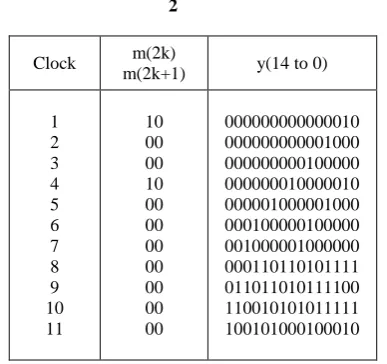
[image:5.595.48.287.644.760.2]Table 3: Data flow table for LFSR with unfolding factor of 2
Clock m(2k)
m(2k+1) y(14 to 0)
1 2 3 4 5 6 7 8 9 10 11
10 00 00 10 00 00 00 00 00 00 00
000000000000010 000000000001000 000000000100000 000000010000010 000001000001000 000100000100000 001000001000000 000110110101111 011011010111100 110010101011111 100101000100010
5.2
Area, Clock Cycle and Power Analysis
The design is analyzed for different levels of unfolding factors in order to discuss the hardware and power overhead involving in different parallelism levels. The power analysis and device utilization analysis is done by implementing this LFSR in XilinxISE9.2i is graphically shown in Figure 7 , 8 and 9.
6740
6760
6780
J=0
J=2
J=3
6757.16
6766.476772.45
Total power(mW)
Figure 7: Comparison of total power for different unfolding factors
0
100
J=0
J=2
J=3
79.2
86.4
93.6
16.01
17.77
18.36
47.98
48.23
46.52
Input power(mW)
Logic power(mW)
Signal power(mW)
Figure 8: Comparison of various powers for different unfolding factors
10
20
30
1
2
3
22
11
8
0
20
40
J=0
J=2
J=3
Exor gate count
Message bits processed per clock cycle
[image:6.595.80.274.85.267.2]Clock cycle
Figure 9: Comparison of Area and Speed parameters for different unfolding factors
[image:6.595.56.278.362.482.2]5.3
Screen Shots
[image:6.595.57.279.534.664.2]Figure 10: LFSR before Unfolding
[image:6.595.313.570.553.629.2]Figure 11: LFSR after Unfolding with J=3
Figure 12: LFSR after Unfolding with J=3
6.
CONCLUSION
which automatically increases the speed but it increases the area and power.
7.
FUTURE WORK
Different-pipelining techniques can be introduced to reduce the critical path of the encoder of BCH. Retiming also can be applied to further increase the speed and to reduce the power consumption and area.
8.
ACKNOWLEDGMENT
The authors acknowledge the contributions of the students, faculty of Velalar College of Engineering and Technology for helping in the design of test circuitry, and for tool support. The authors also thank the anonymous reviewers for their thoughtful comments that helped to improve this paper. The authors would like to thank the anonymous reviewers for their constructive critique from which this paper greatly benefited.
9.
REFERENCES
[1] R. Bez, E. Camerlenghi, A. Modelli, and A. Visconti, “Introduction to flash memory,” Proc. IEEE, vol. 91, no. 4, pp. 489–502, Apr. 2003.
[2] J. Cooke, “The inconvenient truths about NAND flash memory,” presented at the Micron MEMCON Presentation, Santa Clara, CA, 2007.
[3] William Stallings, “Cryptography and Network Security-Principles and Practices, Introduction to Finite Fields”, 3rd edition, 2004.
[4] Ranjan Bose, “Information Theory, Coding and Cryptography”.
[5] K.K.Parhi “VLSI Digital Signal Processing Systems-Design And Implementation”.
[6] Wei Liu, Junrye Rho, and Wongong Sung, “Low- Power High throughput BCH error correction VLSI Design for Multi-Level cell NAND Flash Memories”.
[7] Keshab K. Parhi, ”Eliminating the Fan out Bottleneck in Parallel Long Bch Encoders” in proc IEEE, vol.51.No.3, march 2004.
[8] Chao Cheng and Keshab Parhi, “High-Speed Parallel CRC Implementation Based on Unfolding, Pipelining And Retiming”, in proc, IEEE, vol.53, No.10, October 2006.
[9] Naresh Reddy, B.Kiran Kumar and K.monisha Sirisha,” On the Design of High Speed Parallel CRC Circuits Using DSP Algorithms” in IJCSIT, vol.3 (5), 2012. [10]John G.Proakis Masoud
Salehi,”Digital-Communications-Linear block codes, cyclic codes, BCH codes, Reed-Solomon codes,” 5th
Edition, 2008.
AUTHOR’S PROFILE
Manikandan.S.K has received B.E degree in Electronics and Communication Engineering from Annai Mathammal Sheela Engineering College, Namakkal District, 2003 and M.E – Embedded Systems from Sasthra University, Tanjore District in the year 2006. He is working as a Professor (Sr.Gr.) in the department of EEE, Velalar College of Engineering and Technology, Erode. Currently he is doing Ph.D under Anna University in the area of VLSI Design. He has published three papers in International Journals and presented five papers in National and International Conferences. His areas of interest are Microprocessor and Microcontroller, ARM Processor, VLSI architectures.
Sharmitha.E.K has received B.E degree in Electrical and Electronics Engineering from Anna University, Coimbatore, 2011. She is currently pursuing Master of Engineering in VLSI Design in Velalar College of Engineering and Technology under Anna University, Chennai. She has published one paper in international journal. Her areas of interest in research are VLSI Signal Processing, VLSI architectures.
Nisha Angeline. M has received B.E degree in Electronics and Instrumentation Engineering from the Indian Engineering College, Thirunelveli District in 2003 and M.E –VLSI Design in Kongu Engineering College, Perundurai in the year 2006. She received first rank in PG course for her academic performance. She is working as a Professor (Sr.Gr) in the department of ECE, Velalar College of Engineering and Technology, Erode. Currently she is doing Ph.D under Anna University in the area of VLSI Design. She has published three papers in International Journals and presented five papers in National and International Conferences. Her areas of interest are Digital Electronics, VLSI Architecture, and VLSI Signal Processing.