Electrical and Optical Interconnects for
High-Performance Computing
Thesis by
Meisam Honarvar Nazari
In Partial Fulfillment of the Requirements for the Degree of
Doctor of Philosophy
California Institute of Technology Pasadena, California
2013
c
2013
Acknowledgements
During the course of my graduate studies at Caltech, I was able to experience an enormous amount of educational, professional, and personal growth due to the guidance of many good teachers and support of many friends. This work would not have been possible without either of these.
I have been very lucky to have had the opportunity to work with an excellent research advisor, Prof. Azita Emami-Neyestanak. Her technical expertise, teaching skills, and the unique ability to motivate me through challenging stages of my research have played a key role in my success. Every single meeting with Azita helped me to find my path and go another step forward in my research, and motivated me to learn more. Her enthusiasm and care were the driving forces for the creation of new ideas in this work. She also helped me to improve my public speaking and writing skills. I sincerely thank her for her kindness and patience.
I would also like to especially thank some of the key faculty and researchers that I had the pleasure of working with at Caltech. I am very grateful to my candidacy and oral defense committee, Prof. Ali Hajimiri, Prof. Axel Scherer, Prof. David Rutledge, Prof. Sander Weinreb, and Prof. Hyuck Choo. Particularly, I gratefully acknowledge Prof. Ali Hajimiri and Sander Weinreb for their support in providing me with access to their labs for experiments. I also thank Dr. Firouz Aflatooni for expanding my knowledge of optics and integrated photonics.
Prof. P. P. Vaidyanathan and Prof. Yaser Abu-Mostafa.
The highly academic environment at the University of Tehran helped me to build the required background in engineering and inspired me to pursue my graduate studies abroad. I sincerely thank Prof. Parviz Jabehdar-Maralani, Prof. Jalil Rashed, and Prof. Shams Moha-jerzadeh, for their advice, encouragements and remarkable teaching. The strong knowledge base that I acquired during my Masters studies under supervision of Prof Roman Genov at the University of Toronto greatly prepared me for my Ph.D. research. I would like to thank Roman for his great support and patience in training me.
I have truly enjoyed and greatly benefited from the interaction with an amazing group of research colleagues at Caltech. I would like to thank my friends and colleagues Matthew Loh, Juhwan Yoo, Manuel Monge, Saman Saeedi, Mayank Raj, Krishna Sataluri, Kaveh Hosseini, and Laleh Rabieirad in Azita’s group for their technical support. I extend my gratitude to my friends Amir Safaripour, Kaushik Sengupta, Kaushik Dasgupta, Steven Bowers, Alex Pai, Behrooz Abiri, and Constantine Sideris in Prof. Hajimiri’s group.
I would like to thank my friends Peyman Tavalali, Masoud Farivar, Saeid Farivar, Amin Khajehnejad, Hamed Hamze, Ali Vakili and Sormeh Shadbakht for making Caltech a fun place to live and work.
I wish to thank the National Science Foundation, C2S2, and IFC for their financial support. Also, donated resources from ST Microsystems, CMP, and Cosemi Technologies enabled this research.
I sincerely thank my brothers, Mehdi and Masoud Honarvar Nazari and my sister, Narges Honarvar Nazari for their support that eased the hardship of being away from home. I also would like to thank my other brother and sister (in-law) Amin-Qasem Safarian and Neda Bozorgkhan for providing a wholesome environment and making me feel at home.
Abstract
Technology scaling has enabled drastic growth in the computational and storage capacity of integrated circuits (ICs). This constant growth drives an increasing demand for high-bandwidth communication between and within ICs. In this dissertation we focus on low-power solutions that address this demand. We divide communication links into three sub-categories depending on the communication distance. Each category has a different set of challenges and requirements and is affected by CMOS technology scaling in a different man-ner. We start with short-range chip-to-chip links for board-level communication. Next we will discuss board-to-board links, which demand a longer communication range. Finally on-chip links with communication ranges of a few millimeters are discussed.
receiver can equalize channels with maximum 21dB loss while consuming about 7.5mW from a 1.2V supply. We also introduce a compact, low-power transmitter employing passive equal-ization. The efficacy of the proposed technique is demonstrated through implementation of a prototype in 65nm CMOS. The design achieves up to 20Gb/s data rate while consuming less than 10mW.
An alternative to electrical signaling is to employ optical signaling for chip-to-chip inter-connections, which offers low channel loss and cross-talk while providing high communication bandwidth. In this work we demonstrate the possibility of building compact and low-power optical receivers. A novel RC front-end is proposed that combines dynamic offset modulation and double-sampling techniques to eliminate the need for a short time constant at the input of the receiver. Unlike conventional designs, this receiver does not require a high-gain stage that runs at the data rate, making it suitable for low-power implementations. In addition, it allows time-division multiplexing to support very high data rates. A prototype was imple-mented in 65nm CMOS and achieved up to 24Gb/s with less than 0.4pJ/b power efficiency per channel. As the proposed design mainly employs digital blocks, it benefits greatly from technology scaling in terms of power and area saving.
Contents
Acknowledgements iv
Abstract vii
1 Introduction 1
1.1 Organization . . . 6
2 Electrical Interconnects Background 8 2.1 Metrics of Electrical Links . . . 9
2.1.1 Bit-Rate . . . 9
2.1.2 Bit-Error Rate . . . 10
2.1.2.1 Amplitude Noise . . . 13
2.1.2.2 Timing Noise . . . 15
2.2 Basics of Electrical Links . . . 15
2.2.1 Channel . . . 16
2.2.1.1 Inter Symbol Interference . . . 17
2.2.1.2 Crosstalk . . . 20
2.2.2 Transmitter . . . 23
2.2.2.1 Transmitter Equalization . . . 27
2.2.3 Receiver . . . 31
2.2.3.1 Receiver Equalization . . . 32
2.2.4 Timing Recovery . . . 37
2.3 Summary . . . 41
3 High-Speed Low-Power Electrical Transceivers 43 3.1 Receiver Architecture . . . 44
3.2 Decision Feedback Equalization Implementation . . . 46
3.2.1 Current-Mode Summers . . . 47
3.2.2 Charge-Mode Summers . . . 48
3.2.2.1 4-tap Realization . . . 50
3.2.2.2 Generalization of Switched Capacitor Summers . . . 57
3.2.3 Comparator Design . . . 61
3.3 Far-End Crosstalk Cancellation . . . 62
3.4 Experimental Results . . . 70
3.5 Transmitter Design . . . 77
3.5.1 Transmitter Architecture . . . 77
3.5.2 Experimental Results . . . 81
3.6 Summary . . . 85
4 Overview of High-Speed Optical Links 88 4.1 Optical Channels . . . 90
4.2 Optical Receivers . . . 92
4.2.1 Photodiodes . . . 92
4.2.2 Receiver Front-End . . . 93
4.2.2.1 Transimpedance Amplifiers . . . 94
4.2.2.2 Integrating Front-Ends . . . 100
4.3 Optical Transmitters . . . 105
4.3.1 Vertical Cavity Surface Emitting Laser . . . 105
4.3.2 Mach-Zehnder Modulator . . . 106
4.3.3 Ring Resonator . . . 108
5 Low-Power Optical Receiver Design 111
5.1 Low-Power Double-Sampling RC Front-End . . . 112
5.1.1 Front-End Sensitivity Analysis and Implementation . . . 119
5.2 System-Level Design Considerations . . . 126
5.2.1 Adaptation of Dynamic Offset Modulation . . . 126
5.2.2 Double-Sampling Front-End Scaling . . . 130
5.2.2.1 Sensitivity . . . 131
5.2.2.2 Data Rate . . . 132
5.2.2.3 Power Consumption . . . 132
5.2.2.4 Dynamic Range . . . 133
5.2.3 Photodiode Capacitance Scaling . . . 134
5.2.4 Clocking . . . 136
5.3 Experimental Results . . . 140
5.4 Summary . . . 146
6 On-Chip Wires: Characteristics, Models, and scaling 148 6.1 Wire Characteristics . . . 149
6.1.1 Resistance . . . 150
6.1.2 Capacitance . . . 152
6.1.3 Inductance . . . 153
6.2 Wire Performance Metrics . . . 153
6.2.1 Delay . . . 154
6.2.2 Crosstalk . . . 156
6.2.3 Power . . . 160
6.3 Repeaters . . . 160
6.4 Wire Scaling . . . 169
7 On-Chip Interconnects 173
7.1 On-Chip Communication Power Trend . . . 173
7.2 Prior Art in Design of On-Chip Links . . . 176
7.2.1 Low Voltage Signaling . . . 177
7.2.2 Current-Mode Drivers . . . 179
7.2.3 On-Chip Transmission Line . . . 179
7.2.4 Equalization . . . 181
7.3 Double-Sampling Link . . . 182
7.3.1 Receiver Design . . . 182
7.3.2 Transmitter Design . . . 183
7.4 Link Latency . . . 187
7.5 Circuit Implementation . . . 188
7.6 Experimental Results . . . 190
7.7 Summary . . . 195
8 Conclusions 197 8.1 Electrical Interconnects . . . 197
8.2 Optical Link Performance Summary . . . 199
8.3 On-Chip Interconnects . . . 201
References 202
List of Figures
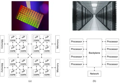
1.1 Examples of complex electronic systems. A high-performance multi-core
pro-cessor (a). A computer server (b). . . 2
1.2 History of microprocessor performance scaling. . . 3
1.3 IO bandwidth requirement of microproccesors in recent years (a). Constant growth of the required IO bandwidth according to ITRS (b). . . 3
2.1 Fan-out of four inverter chain . . . 10
2.2 FO-4 delay metric for different technology nodes (a), and fT−1 versus FO4 met-ric, which shows a linear relation (b). . . 11
2.3 Illustration of a data eye. (a) shows a noisy data stream, and (b) shows the folding of the data stream into a data eye. . . 11
2.4 Effect of amplitude noise in (a) and timing noise in (b) on the eye diagram quality. . . 12
2.5 Translation of the eye-diagram to bathtub curve as a tool to measure signal integrity. . . 13
2.6 Diagram of bit error rate versus signal to noise ratio. . . 14
2.7 Components of an electrical communication link. . . 16
2.8 A typical backplane link and its components [22]. . . 16
2.9 Transfer characteristics of typical backplane channels with and without via stubs at different lengths [22]. . . 17
2.10 Pulse response of a typical bandwidth-limited backplane channel illustrating dispersion. . . 18
2.12 Far-end and near-end crosstalk in coupled transmission lines. . . 20 2.13 Lumped equivalent model for coupled transmission lines. . . 21 2.14 Effect of coupling on even and odd modes, which results in data dependent jitter. 24 2.15 Effect of coupling on the victim signal amplitude when the transmitted
aggres-sor and victim signals are not synchronized. . . 24 2.16 Voltage-mode and current-mode transmitter design. . . 25 2.17 Different transmitter examples, (a) voltage-mode, (b) single-ended current mode,
(c) differential current-mode. . . 26 2.18 Transmitter pre-emphasis using high-frequency boosting. . . 27 2.19 Block diagram of a transmitter with m-tap FIR-based equalization. . . 28 2.20 Pulse response of a channel before and after 2-tap transmitter FIR equalization. 29 2.21 Eye diagram at the end of a lossy channel using a transmitter with no tap of
FIR equalization as well as 1-tap and 2-tap of equalization. . . 30 2.22 Transmitter equalization through high frequency boosting to achieve flat response. 30 2.23 Different high-frequency boosting configurations. . . 31 2.24 A typical electrical receiver block diagram. . . 32 2.25 Simplified block diagram of a decision feedback equalizer. . . 33 2.26 Loop-unrolling of the first tap of the DFE to remove the critical feedback loop. 34 2.27 Feed-forward equalization at the receiver. . . 35 2.28 Continuous-time receiver equalization using frequency dependent source
degen-eration. . . 36 2.29 Passive high-pass filter equalizer (a). Dual path continuous-time equalizer (b). 36 2.30 Clock recovery at the receiver. . . 38 2.31 CDR phase detectors: (a) linear [51], (b) binary [52] . . . 39 2.32 Simple binary (1bit/symbol) and PAM-4 (2bits/symbol) modulations. . . 40
3.2 Top level architecture of the proposed receiver employing half-rate clocking and loop-unrolling. . . 46 3.3 Current-mode summer employed in conventional DFE (a). Current-integrating
summer (b). Operation of the current-integrating summer (c). . . 49 3.4 (a) Circuit-level implementation of the front-end S/H/summer operating in
two phases: (b) sample/sum phase, (c) sum/hold phase (single-ended version is shown for simplicity). . . 51 3.5 S/H/summer performance in the case of n=2. S/H/summer voltage loss,Asampler
(a). SNR at the output of the S/H/summer (b). SNR normalized to clocking power consumption (c). To achieve high SNR (hence high BER) and power ef-ficiency while maintaining the DFE speed, CS1 and CS2 are chosen to be equal
to 19fF and 14fF, respectively. . . 54 3.6 Simulated input eye diagram for a 5” FR-4 trace at 15Gb/s. Red and green
circles show the sampled input before and after 2-tap decision feedback equal-ization, respectively (a). Histogram of the sampled input before and after equalization. 2-tap DFE improves eye opening from 2mV to 40mV (b). . . 56 3.7 4-bit current steering DAC that generates DFE tap coefficients. . . 56 3.8 Switched capacitor summer for 2n-tap, sample/sum phase (a), sum/hold phase
(b). . . 57 3.9 Signal gain comparison between SC and current-mode summer (a). Normalized
SNR for the SC and current-mode summer (b). Tap coefficient gain for different number of taps (c). . . 59 3.10 Linearity of the post-cursor taps for an eight-tap (a) switched capacitor and
(b) current-mode summer. . . 60 3.11 2-tap DFE architecture with loop-unrolling. . . 62 3.12 Combined analog MUX and latch with cross-coupled capacitors to reduce
kick-back. . . 63 3.13 Crosstalk cancellation technique employing a high-pass filter as a differentiator
3.14 Measured transfer characteristics of a 5” long, 32mil wide coupled trace with 40mil separation (a). Simulated FEXT noise due to a 15Gb/s pulse and the emulated FEXT employing the differentiator along with the residual FEXT noise (b). . . 64 3.15 Simulated output of the S/H/summer before and after applying the aggressor
as well as when the crosstalk cancellation is enabled. . . 65 3.16 Crosstalk cancellation technique for multiple coupled channels. . . 67 3.17 Simulated channel, adjacent FEXT, and distant FEXT response for width=32mil,
spacing=48mil, and length=10”, (d) for length=20”. (e) Residual crosstalk from the adjacent aggressor after cancellation normalized to the FEXT energy along with the distant FEXT for 10” channel, and (f) 20” channel.. . . 68 3.18 Effect of loading due to the crosstalk cancellation circuitry on the overall
chan-nel insertion loss for a 10” chanchan-nel (a) and a 20” chanchan-nel (b). . . 69 3.19 The die micrograph of the receiver with major blocks highlighted. . . 71 3.20 Receiver DFE and crosstalk cancellation test set-up. . . 71 3.21 CMOS clock generation through CML-to-CMOS conversion followed by duty
cycle correction. . . 72 3.22 Channel transfer characteristics for 5”, 10” and 18” PCB traces. . . 72 3.23 The PRBS7 eye diagram at the receiver input and the bathtub curve after
equalization for, (a) 11Gb/s data over 18” trace, (b) 13Gb/s data over 10” trace, (c) 15Gbs data over 5” trace. . . 74 3.24 Receiver power breakdown. . . 75 3.25 The receiver bathtub curve without and with crosstalk noise, and after crosstalk
cancellation for, (a) 8Gb/s, (b) 10Gb/s, (c) 11Gb/s, and (d) 12.5Gb/s victim and aggressor data. . . 76 3.26 Shunt and double-series bandwidth enhancement technique, which requires
3.29 Transistor-level schematic of the transmitter employing segmented T-coils. . . 80 3.30 Simulation results showing the programmable high frequency peaking achieved
by RC source degeneration. . . 81 3.31 Simulated transfer characteristics of the transmitter and channel for different
levels of pre-emphasis, (a) 5” FR4 channel, (b) 10” FR4 channel. . . 82 3.32 Transmitter die micrograph along with the core layout. . . 82 3.33 Transmitter measurement setup for characterizing the performance over
differ-ent channels . . . 82 3.34 20Gb/s on-chip PRBS-7 generator. . . 83 3.35 Channels’ transfer characteristic. . . 84 3.36 The transmitted 10Gb/s PRBS7 data over 5” FR4 channel with about 10dB loss
at Nyquist, before equalization (a), over equalized (b) and optimally equalized (c). . . 84 3.37 Transmitter output at 15Gb/s over lossy channel with 7dB loss. . . 85 3.38 Output of the channel before and after equalization with the 2-tap FIR equalizer
and continuous-time equalizer for 15Gb/s data over 5” channel (a), 15Gb/s data over 10” channel (b), and 20Gb/s data over lossy channel (c). . . 86
4.1 Optical signal transmission over fiber. . . 89 4.2 An optical fiber cross-section with the core and cladding having refractive index
of n1 and n2, respectively to allow for total internal reflection. . . 90
4.3 Cross section of a polymer waveguide. . . 92 4.4 Electrical model of a photodiode. . . 93 4.5 Simple resistive receiver front-end performing current to voltage conversion. . 94 4.6 Schematic of a common-gate TIA (a) and a regulated cascode TIA (b). . . 95 4.7 Typical shunt-shunt feedback TIA (a). Simplified small signal model of the
4.10 TIA data rate (a) and power consumption (b) as a function of transimpedance. 99
4.11 Sensitivity degradation as a result of data rate scaling. . . 100
4.12 Integrating optical front-end employing balanced photodiode and an inverter. 101 4.13 Integrate and reset front-end. . . 102
4.14 Double-sampling front-end with a DC current to provide bipolar voltage differ-ence for a one and a zero. . . 103
4.15 Double-sampling integrating front-end. . . 104
4.16 Input demultiplexing receiver using multiple sampler clock phases. . . 104
4.17 Typical current-mode VCSEL driver . . . 106
4.18 A Mach-Zehnder modulator comprising of two arms which introduce different phase shifts to the optical signal in order to perform amplitude modulation. . 107
4.19 A ring resonator with pn structure for performing resonant wavelength shift enabling optical amplitude modulation. . . 109
5.1 Different optical receiver architectures. (a) simple resistive front-end, (b) tran-simpedance front-end with limiting amplifiers, (c) integrating double-sampling receiver. . . 112
5.2 The proposed RC double-sampling front-end architecture (a). The exponential input voltage and the corresponding double-sampled voltage for a long sequence of successive ones (b). . . 115
5.3 Modified RC front-end with DOM to resolve input dependent double-sampled voltage (a). The basic operation of DOM technique (b). . . 117
5.4 Block diagram of the offset modulation technique (a). The first sample is sub-tracted from the double-sampled voltage, ∆V[n], to make it constant regardless of the input sequence. Simulated operation of the DOM for a long sequence of ones showing ∆V[n] before and after DOM (b). . . 118
5.5 Top level architecture of the RC double-sampling front-end. . . 120
5.7 Schematic showing the noise sources in the front-end (a). This plot shows how the clock jitter is translated into the double-sampled voltage noise (b). There is an optimum range, 15-25fF, for the sampling capacitor to achieve maximum
SNR (c). . . 123
5.8 Basic operation of the DOM gain, β, adaptation algorithm. The error signal is generated for a certain pattern depending on the difference between ∆V[n] and ∆V[n−1]. . . 127
5.9 The input waveform and β error detection (a), modified sense-amplifier as the difference comparator (b), samplers and comparators for error detection (c), bang-bang β adaptation loop (d). . . 128
5.10 Simulated performance of the front-end before (a) and after (b) DOM adapta-tion. Gaussian noise with σ=10mV is applied at the sampler. . . 129
5.11 Optimum sampling capacitor size, CS versus the photodiode capacitance, CP D. 131 5.12 Receiver current sensitivity versus photodiode capacitance, with and without scaling sampling capacitor (a). Receiver data rate versus photodiode capaci-tance for 100µA sensitivity (b). . . 135
5.13 2x-oversampled phase detection for the proposed receiver. . . 136
5.14 The input waveform and baud-rate phase detection, for in-phase (a), and out of phase clock (b). . . 137
5.15 Electrical measurement setup. . . 138
5.16 Photodiode current emulator. . . 139
5.17 Receiver sensitivity characteristics for different data rates. . . 140
5.18 Current and voltage sensitivity versus data rate. . . 141
5.19 Power consumption and efficiency at different data rates. . . 141
5.20 The receiver power breakdown. . . 142
5.21 Optical test set-up. . . 142
5.22 Micrograph of the receiver with bonded photodiode (a). Coupling laser through fiber to the photodiode (b). . . 144
5.24 Optical sensitivity at different data rates. . . 145
5.25 Comparison between voltage sensitivity for electrical and optical measurement. 146 6.1 On-chip interconnect length trend. . . 149
6.2 On-chip metal stack in different technology nodes, 130nm (a), 65nm (b), and 32nm (c). . . 150
6.3 The schematic profile of diffusion barrier layer (a). SEM cross section of the diffusion barrier layer [171] (b). . . 151
6.4 A simple capacitance model for on-chip wires. . . 152
6.5 Transition time (tr) versus the length of the interconnect line (l). The crosshatched area denotes the region where inductance is important. . . 154
6.6 Simple lumped model for an RC dominated wire. . . 155
6.7 Simple model for evaluating capacitive coupling. . . 157
6.8 Capacitive coupling model in a wire with considerable resistive loss. . . 157
6.9 Techniques to combat capacitive coupling in on-chip wires. . . 158
6.10 Differential signaling along with wire twisting to remove crosstalk. . . 159
6.11 Ground shield insertion to avoid croostalk. . . 160
6.12 Inserting repeaters to improve on-chip wire delay. . . 161
6.13 A segment of a repeated wire represented by a π-model. . . 162
6.14 Delay of the repeated wire normalized to the optimal delay (a). The constant delay contours as a function of the repeater normalized width and wire segments relative to optimal values. . . 165
6.15 Constant power contours along with delay contours illustrating the trade-off between power and delay. . . 166
6.16 Constant power-delay product contours. . . 166
6.17 Eye diagram when 10-to-90% rise time equal to the bit time. . . 167
6.18 Constant rise time contours for a repeated wire. . . 168
6.19 Constant rise time along with power contours. . . 169
6.21 Unrepeated global and semi-global wires delay normalized to FO-4 inverter delay for different technologies. . . 170 6.22 Repeated global and semi-global wires delay normalized to FO-4 inverter delay
for different technologies. . . 171
7.1 Repeated and un-repeated wire delay variation trend with CMOS technology scaling. . . 174 7.2 The repeater distance and number of repeaters for an optimally repeated wire
in different technology nodes. . . 175 7.3 Projection of the repeated wire power consumption in different technology nodes.176 7.4 Dynamic power breakdown for a single core processor [178]. . . 177 7.5 Charge-recycling stacked transmitter employed to reduce effective supply voltage.178 7.6 Current-mode on-chip wire drivers. . . 180 7.7 Sense amplifier based current-mode on-chip wire driver. . . 180 7.8 Receiver top-level architecture, double-sampling technique and DOM. . . 184 7.9 Z-domain representation of the double-sampler and the dynamic offset
modu-lation (a). Operation of the dynamic offset modumodu-lation (b). . . 185 7.10 Capacitively-driven transmitter (a), double-sampling technique to resolve the
received data (b). . . 186 7.11 Frequency characteristics of a minimum-pitch 7mm wire along with the power
spectral density of the double-sampled pulse. . . 187 7.12 Power spectral density of the transmitted pulse and the double-sampled pulse. 188 7.13 Transistor level schematic of the receiver front-end and the StrongArm sense
amplifier with capacitive offset cancellation. . . 189 7.14 Shielded single-ended on-chip wire (a). Simulated and measured characteristics
of the on-chip wires (b). . . 191 7.15 Die micrograph. . . 192 7.16 Total power consumption of the receiver and the transmitter for the 4mm,
7.17 Power breakdown for the 5mm, and 7mm links at different data rates. . . 193 7.18 Crosstalk measurement setup. . . 194 7.19 Power consumption of the 4mm link in the presence of an aggressor at different
List of Tables
3.1 DFE PERFORMANCE SUMMARY . . . 74
3.2 CROSSTALK CANCELLATION PERFORMANCE SUMMARY . . . 75
3.3 TRANSMITTER PERFORMANCE SUMMARY . . . 85
5.1 OPTICAL RECEIVER PERFORMANCE SUMMARY. . . 146
6.1 PERFORMANCE OF ON-CHIP WIRES IN 28nm TECHNOLOGY. . . 156
Chapter 1
Introduction
Figure 1.1: Examples of complex electronic systems. A high-performance multi-core processor (a). A computer server (b).
leaves the increase in per pin bandwidth as the only solution to the future I/O bandwidth problem.
Figure 1.2: History of microprocessor performance scaling.
higher aggregate data rate. One of the consequences of this approach is the excessive capac-itive and inductive coupling between adjacent channels, which manifests itself as crosstalk noise. Crosstalk can also severely degrade signal integrity. The effect of ISI and crosstalk will be explained in more detail in the next chapter. A common approach in the design of high-speed serial links over bandwidth-limited channels is to employ equalization techniques to cancel destructive effects of ISI. Typical equalization techniques include decision feedback equalization (DFE) [64–67], feed-forward equalization (FFE) [43–47] and continuous time linear equalization [68–71] at the receiver and FFE at the transmitter [33–37]. These tech-niques can be used in parallel links with many IOs to increase the aggregate data rate. A number of techniques have been also proposed to remove the effects of crosstalk. The design in [73] employs an FFE equalizer and [76] uses crosstalk-induced jitter equalization at the receiver. Other approaches to compensate for crosstalk noise include the use of staggered I/Os [77] or a finite-impulse response (FIR) filter at the transmitter [78]. All these schemes result in significant power consumption and are not suitable for parallel data links. This dissertation provides a compact low-power electrical link architecture with crosstalk can-cellation capability to enable scaling of chip-to-chip communication bandwidth. The main emphasis of the proposed design is low-power consumption, small area and scalability to future technologies.
optical signaling can potentially close the gap between the interconnect speed and on-chip data processing speed. This dissertation investigates the challenges of designing electronics for short-haul optical links and proposes a number of solutions to enable optical IOs. We focus on techniques to design simple, compact and low-power receivers suitable for dense parallel optical interconnects.
Hybrid integration of optical devices with electronics has been demonstrated to achieve high performance [89, 129–134], and recent advances in silicon photonics have led to fully integrated optical signaling [135, 136]. These approaches pave the way to massively parallel optical communications. In order for optical interconnects to become viable alternatives to established electrical links, they must be low cost and have competitive energy and area efficiency metrics. Dense arrays of optical detectors require very low-power, sensitive, and compact optical receiver circuits. Existing designs for the input receiver, such as TIA, require large power consumption to achieve high bandwidth and low noise, and can occupy large area due to bandwidth enhancement inductors. Moreover, these analog circuits require extensive efforts to migrate and scale to future technologies. Therefore, in this thesis we develop techniques to implement low-power, compact receiver circuits for highly parallel optical communication.
As VLSI technologies continue to scale, on-chip wires will present increasing latency and energy problems. While circuit performance benefits from technology scaling, the shrinking cross-sectional area of the on-chip wires increases electrical resistance and hence latency. Repeaters mitigate the latency problem but do little to improve the energy cost. Moreover, as technology scales, the number of repeaters grows significantly, which increases power consumption and adds complexity. A CMOS wire driver running at an effective frequency
f must switch a total wire capacitance Cw through the voltage Vdd, leading to a power
cost proportional to Cwf Vdd2. Under technology scaling, wire capacitance remains largely
constant (for global wires spanning constant-sized die), Vdd scales down only slowly, while
may carry in excess of 250 meters of wiring interconnect, which would burn nearly 50 W of wire and repeater power at 4 GHz [183]. Designers have proposed different techniques to mitigate the power and latency problem of the on-chip wires. Low-swing differential signaling [179, 182–185, 191], current-mode signaling [186, 187, 192], equalization [185, 191] and transmission lines [179, 186] have been employed to resolve the energy and latency problem of the repeated links. However, these techniques are becoming less adequate in meeting bandwidth density and power requirements. In this thesis we have attempted to provide a solution that maximizes bandwidth density for on-chip communication in a power and area efficient manner.
In summary, this dissertation provides solutions to enable increasing data rate both for chip-to-chip and on-chip communications with the emphasis on low power consumption to meet the ever-increasing demand for the bandwidth required by future microprocessors.
1.1
Organization
rate. It is shown that the proposed crosstalk cancellation technique operates efficiently with minimal power overhead.
As the communication distance increases to tens of inches, the efficiency of equalization technique drastically degrades due to the increase in the number of equalization taps required to compensate for the excessive channel loss. This makes electrical links inadequate in meeting the bandwidth requirement for long communication distances. In addition optical links can have significant advantages over electrical links if a large number of parallel optical channels can interface with each IC. For parallel optical interconnects, the design of a low-power receiver front-end is particularly challenging. In Chapter 4 we provide an introduction to chip-to-chip optical communication links with an emphsis on optical receivers. This chapter continues with exploring the prior art and investigating their challenges in meeting the requirements for highly parallel high data rate optical links. Chapter 5 of this thesis focuses on the receiver design for chip-to-chip optical interconnects. It is shown that a promising solution to these challenges is an RC front-end which employs double-sampling as well as dynamic offset modulation techniques. Unlike most prior designs, this receiver avoids high-gain analog blocks that operate at the the input data-rate. The eventual goal in optical interconnect design is to have thousands of transceivers in a single chip. Scaling of parallel optical interconnects to hundreds and thousands of links on a single chip requires receiver and transmitter circuitries that are very compact and have very low power consumption at high data rates. The proposed design was implemented in a test-chip fabricated in 65nm CMOS technology. Measurement results from this test-chip show that the proposed design achieves low-power consumption at high data rates while achieving good sensitivity for hybrid integrated solutions which offer moderate parasitic capacitance in the range of 100-200fF.
In Chapter 6 of this dissertation we take a close look at on-chip wires scaling and inves-tigates the challenges of on-chip signaling in highly-scaled technologies. Then in Chapter 7, we will introduce a novel technique inspired by the optical receiver introduced in Chapter 5 in conjunction with low-swing signaling techniques to mitigate these challenges in a power and area efficient manner.
Chapter 2
Electrical Interconnects Background
2.1
Metrics of Electrical Links
A link’s performance can be evaluated based on several factors. For exploring the maximum data rate of a given technology, two metrics in particular are used to evaluate various designs: the bit-rate (or its inverse, the bit-time) and the bit-error rate (BER). To get a better sense of how bit-rate changes with scaling we normalize it by the speed of the CMOS technology. The normalization factor is the delay of a loaded inverter, as described in the next section.
Since a link’s receiver needs to convert an analog signal back into digital data, there is always a probability for errors to occur. Bit-error rate (BER) indicates the reliability of the link in data communication links. A link’s maximum data rate is usually specified at a specific BER (e.g. 10−12) to guarantee the robustness of the overall system. The following section describes how errors occur due to voltage or timing noise. To illustrate the effect of noise on the system performance, the BER is shown as a function of the signal-to-noise ratio (SNR) in a simplified analysis.
2.1.1
Bit-Rate
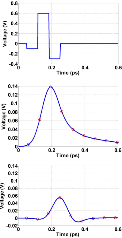
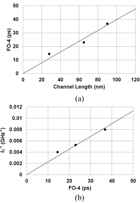
The minimum bit-time varies with the CMOS process technology. It is useful to employ a metric to represent the bit-time that is independent of technology to facilitate performance extrapolation to future technologies. An appropriate metric is the delay of a buffer driving a normalized load. A “FO-4” delay is the delay of one stage in a chain of inverters, in which each inverter is driving another inverter with 4X larger size, as shown in Figure 2.1. In other words, each of the inverters in the chain drives a capacitive load (fan-out) that is 4X larger than its input capacitance. The delay of various circuits can be normalized to FO-4 delay in a certain technology.
This metric is applicable based on the observation that the delays of topologically different CMOS digital circuits scale by approximately the same factor [17]. Figure 2.2 shows the actual FO-4 delay for various technology nodes. It is interesting to note that a reasonable estimate for FO-4 delay is roughly 400ps/µm of effective channel length and, conversely, the
Figure 2.1: Fan-out of four inverter chain
relation between this metric and the maximum achievable data rate in a certain technology node. As a result, by migrating from one technology to another, in theory the maximum data rate improves due to the smaller FO-4. It should be also noted that the increase in data rate makes data transmission difficult over electrical channels. This will be discussed in the remainder of this chapter in more detail.
2.1.2
Bit-Error Rate
One of the most important metrics for performance of a link is the bit-error rate, BER, which indicates the reliability of the link. This reliability ties closely with the data-rate as excessive errors may force a link to operate at a lower data rate. The errors are due to noise on the signal that is transmitted and the noise in the receiving circuits as well as the noise introduced by the channel. The noise can be divided into timing noise and amplitude noise. The effect of noise is often illustrated using a data eye. Figure 2.3 shows how a data eye is created by folding a signal waveform into a single bit-time. For a noise-less signal, the horizontal and vertical eye opening are at their maximum. Noise on the bit stream results in a reduced eye opening, making the signal more difficult to be resolved at the receiver.
Figure 2.2: FO-4 delay metric for different technology nodes (a), and fT−1 versus FO4 metric, which shows a linear relation (b).
Figure 2.4: Effect of amplitude noise in (a) and timing noise in (b) on the eye diagram quality.
the decision level could make data resolution more sensitive to error by reducing the voltage noise margin for a one versus a zero, or vice versa. Figure 2.4(b) shows the effect of both timing offset and timing jitter. Static timing error is the fixed offset in the sample position from the ideal position, Tos. Dynamic timing jitter is due to the random noise in the phase
position. The resulting timing margin, Tmargin, can be calculated as
Tmargin=Tb−Tos−Tjd−Tjc, (2.1)
where Tb is the bit time, and Tjd and Tjc are the jitter on the data transitions and the
sampling clock, respectively. Since the sampling position is defined with respect to the data transition and the clock and data jitter are two independent random processes, jitter on both the clock and the data additively reduces the timing margin. With ideal square pulses, as long as the sum of the magnitudes of the static and dynamic timing errors is less than a bit-time, the sampled value will always be the correct bit. However, because of finite signal slew rates, timing errors that are less than a bit-time can reduce the amplitude of the signal at the sample point hence affecting the BER.
Figure 2.5: Translation of the eye-diagram to bathtub curve as a tool to measure signal integrity.
system. We will discuss the effect of these noise sources on the performance of the system in the next two sections.
In addition to the eye diagram, the bathtub curve is another diagnostic tool for performing signal integrity analysis. Bathtub curves are usually created by measuring the BER while sweeping the sampling clock over the bit time. Figure 2.5 shows a typical bathtub curve. Bathtub curves are useful tools for characterizing the performance of the receiver and show how tolerant the system is to the sampling clock jitter noise, as well as the amount of horizontal and vertical eye opening. We will be using bathtub curves to characterize electrical receivers in the next chapter.
2.1.2.1 Amplitude Noise
Figure 2.6: Diagram of bit error rate versus signal to noise ratio.
decision. This probability determines the bit-error rate. The BER indicates how many errors are likely to occur for a certain number of resolved bits. This rate often depends on the amount of signal power and the amount of noise power.
For instance, the probability of error due to a noise with Gaussian distribution can be expressed as a function of the signal-to-noise ratio (SNR) in case of an equiprobable one or zero [19]:
Perror =
Z ∞
A
1 2πσ2
n
exp(− x 2
2σ2
n
)dx= 1−Q(A
σn
) = 1−Q(SN R), (2.2)
where A is the signal amplitude, σn is the standard deviation of the noise, and Q(x) is the
Q-function and represents the tail probability of the standard normal distribution. Figure 2.6 shows how the BER changes with SNR considering the above model. Increasing the signal amplitude will increase SNR, and hence improve the BER.
levels. A decision level shifted higher by αA would reduce the amplitude of a one and increase the amplitude of a zero. In case of equiprobable one and zero, the probability of error is the average of the two probabilities. Since the probability increases exponentially with decreasing SNR, the error rate is dominated by the signal value with the lower SNR which, in this case, is due to the one. This reduction in performance can be expressed as an SNR penalty of 20log10(1−α).
2.1.2.2 Timing Noise
Timing noise can similarly affect the link’s performance. Timing noise can have a noise distribution similar to the amplitude noise. If the magnitude of the timing error exceeds half the bit-time, the receiver would sample the previous or next bit instead of the current bit, resulting an error. The probability of the noise exceeding Tb
2 determines the minimum
BER independent of the signal amplitude. Typically the timing noise does not scale with decreasing the bit-time, which results in increasing the minimum BER.
In addition to affecting the minimum BER, phase errors can affect SNR. As seen in Figure 2.4(b), sampling away from the peak of the waveform results in a sampled value that is less than the peak signal amplitude. Also, due to the finite rise and fall time of the input data, timing noise effectively results into amplitude noise and hence reduces the SNR.
2.2
Basics of Electrical Links
Figure 2.7: Components of an electrical communication link.
Figure 2.8: A typical backplane link and its components [22].
2.2.1
Channel
As the data rate keeps increasing to meet the bandwidth requirement for today’s systems, the filtering imposed by the electrical channel becomes the most challenging problem. The performance of the channel strongly depends on the application. As an example a typical backplane link and its components are shown in Figure 2.8 [20, 21]. Loss per unit length of PCB-traces increases with the frequency due to the dielectric loss and skin effect. Different trace lengths and backplane material properties, as well as types of connectors, vias and routing layers, cause significant variation in channel transfer characteristics.
Figure 2.9: Transfer characteristics of typical backplane channels with and without via stubs at different lengths [22].
as a low-pass filter. The filtering effects lead to a spread of narrow pulses originally confined to a bit-period as shown in Figure 2.10, which is referred to as pulse dispersion. The tail of the pulse acts as an additive noise for the next bits and is referred to as inter-symbol interference or ISI. Dispersion is enhanced by the filters formed by unintended transmission line impedance discontinuities caused by via stubs and connections. In the time domain these discontinuities cause reflections, which also lead to ISI. Crosstalk is the other problem that occurs in dense interconnects. Both far and near end cross-talk (FEXT and NEXT), are important in such systems.
2.2.1.1 Inter Symbol Interference
Figure 2.10: Pulse response of a typical bandwidth-limited backplane channel illustrating dispersion.
as
RAC(f) =
2.16×10⁻⁶
πD
p
prf , (2.3)
where D is the wire diameter and pr is the relative resistivity of the wire material compared
to copper [23].
Dielectric loss is related to the energy loss in the dielectric surrounding the transmission line. This loss increases proportionally to signal frequency [23]
σD =
πsqrtr
c f tanδ, (2.4)
where tanδis the loss tangent,cis the speed of light andrris the relative permitivity. Due to
the linear dependence on frequency, the dielectric loss dominates over the skin-effect at high frequencies. The crossover frequency depends on the material properties and dimensions of the trace, for instance, the crossover occurs at around 500 MHz for FR4 material [24].
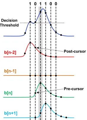
Figure 2.11: Channel dispersion resulting in pre- and post-cursor ISI.
reducing the eye opening at the receiver, hence degrading the overall BER. This problem is exacerbated as the data rate increases.
As discussed earlier, another source of ISI is reflection due to impedance discontinuities. A signal transitioning from one transmission line with characteristic impedance of Z1 to
another line with different impedance, Z2 experiences a reflection of magnitude
R= Z1−Z2
Z1 +Z2
. (2.5)
Figure 2.12: Far-end and near-end crosstalk in coupled transmission lines.
at the receiver or the transmitter side. It can be also created by via stubs on the board that carry signal from one metal layer to another. The stub acts as a capacitor, which reflects high frequency energy. Another dominant source of reflection is the frequency dependent impedance discontinuity due to parasitic device capacitance at both the transmitter and receiver.
2.2.1.2 Crosstalk
As the demand for communication bandwidth increases, link designers start to use more and more channels in parallel to increase the aggregate data rate. Placing channels in close proximity causes electromagnetic coupling between them, which can result in crosstalk interference. Crosstalk can be divided into far-end (FEXT) and near-end (NEXT). As shown in Figure 2.12, FEXT occurs when the aggressor signal travels in the same direction as the victim. The NEXT occurs when the aggressor signal travels in the opposite direction, and can be much more critical as the victim signal is severely attenuated due to the channel loss. Since crosstalk is caused either by capacitive or inductive coupling of different signal lines it has high attenuation at low frequencies. Due to the low-pass filtering of the channel, FEXT is also attenuated at high-frequencies. Therefore FEXT is mostly band-pass, while NEXT is high-pass.
Figure 2.13: Lumped equivalent model for coupled transmission lines.
lines, where CS and Cm represent the self and mutual capacitances of the transmission line
per unit length, respectively, and LS and Lm represent the self and mutual inductances per
unit length, respectively. From the equivalent circuit, the voltage and current relation of the coupled lines can be described as
d dz v1 v2 =
LS Lm
Lm LS
× d dt i1 i2
, (2.6)
d dz i1 i2 =
Ct −Cm
−Cm CS
× d dt v1 v2
, (2.7)
where Ct =CS +Cm. Equations 2.6 and 2.7 show that the current change at the aggressor
the aggressor line causes the capacitively-coupled current change in the victim line. Using the weak coupling assumption [25], it can be shown that the near-end and far-end crosstalk can be calculated as
VF EXT =
1 4(
Cm
Ct
+ Lm
LS
)(V(t)−V(t−2tf)), (2.8)
VF EXT =
1 2(
Cm
Ct
−Lm
LS
)tf
dV(t−tf)
dt , (2.9)
whereV(t) is the driven pulse, andtf is the time of flight along the coupled lines. It should be
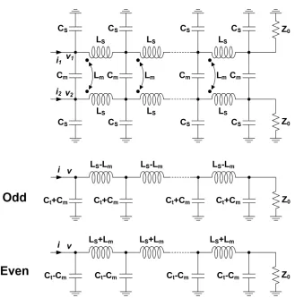
noted that these equations are valid in the case of matched terminated lossless transmission lines. For lossy transmission lines, the above equation can still be used when corrected by the attenuation. In addition, these equations only signify the effect of the crosstalk on the received amplitude of the voltage at both ends of the victim line. Another way that crosstalk manifest itself is through inducing timing jitter [25]. Solutions to Equations 2.8 and 2.9 can be decomposed into two modes, the even and odd modes. The even and odd modes effectively see two different coupling mechanisms. For the even mode, the coupling capacitance has no effect in the signal propagation and as the two lines are carrying the same current, the effective inductance is LS +Lm, whereas for the odd mode, the effective capacitance and
inductance are CS+Cm and LS −Lm, respectively. As a result, the propagation constant
for these two modes can be expressed as [26]
βo =ω
p
(LS−Lm)(Ct+Cm), (2.10)
βe =ω
p
(LS+Lm)(Ct−Cm), (2.11)
tf o =l
p
(LS−Lm)(Ct+Cm), (2.12)
tf e =l
p
(LS+Lm)(Ct−Cm). (2.13)
The speed of the two modes are equal if Lm/LS=Cm/Ct. This condition is held in a
homogeneous transmission line, such as a stripline. For microstrip lines, homogeneity is not guaranteed as the electric and magnetic fields are not symmetric above and below the line due to the surrounding air. The main effect of this difference in the time of flight for even and odd modes is the generation of crosstalk-induced jitter. This phenomena is shown in Figure 2.14. As seen for different cases of the aggressor and victim signal transition, the time of flight for both lines changes. For instance, when both signals transition in the same direction, it is different from when they transition in opposite directions.
It should be noted that in the above analysis we assumed that both victim and aggressor signals transition at the same time. This resulted in data dependent jitter due to the differ-ence between the time of flight for the even and odd modes. However, in a real system it is likely that the transition on the victim and aggressor signal does not happen at the same time. For instance, Figure 2.15 illustrates the case in which the aggressor signal transitions in the middle of the bit time of the victim signal [27]. This will create amplitude noise in the victim signal, which according to Equation 2.9 is proportional to the derivative of the aggressor signal for a far-end channel. This type of crosstalk directly affect the SNR at the receiver, while in the other type, it affects the timing margin.
2.2.2
Transmitter
Figure 2.14: Effect of coupling on even and odd modes, which results in data dependent jitter.
Figure 2.16: Voltage-mode and current-mode transmitter design.
to correctly resolve the data value. Ground level is usually used as the common voltage reference for data resolution. The signal transmission over the line can be done with either a voltage-mode driver or a current-mode driver, shown in Figure 2.16.
In voltage-mode drivers, switches are employed to alternate the line voltage between zero and one, as shown in Figure 2.17(a). Because the switches are implemented with transistors, the driver appears as a switched resistance. To switch the voltage fully, a small resistance is needed, which typically requires a large switching device. In contrast, current-mode drivers are switched current sources, where the output signals are generated via a current source that turns on and off depending on the transmitted data, Figure 2.17(b). The voltage swing at the output depends on the termination and the size of the current source. In order to control the voltage swing and proper termination, to avoid reflections, the current source should be kept in the saturation region and the termination resistor should be carefully designed and controlled [28–30].
Figure 2.17: Different transmitter examples, (a) voltage-mode, (b) single-ended current mode, (c) differential current-mode.
For better supply-noise rejection, the outputs can be driven differentially, as shown in Figure 2.17(c), as it appears as a common-mode noise. Since the current remains roughly constant, the transmitter also induces less switching noise on the supply which could benefit other sensitive circuits on the same chip. However, the static current in this configuration makes it quite power hungry.
To reduce reflections at the transmitter side, it should be designed such that the output resistance properly serves as the termination resistor. An on-chip resistor can be incorporated with current-mode drivers to act as the source termination resistor [31]. Given the fact that the current source introduces a fairly large output resistance when biased in saturation, the overall output resistance would be almost equal to this termination resistor. In the case of voltage-mode drivers, the design is slightly more complex because the switch resistance should match the line impedance. This may be done either through proper sizing of the driver [32] or by oversizing the driver and compensating with an external series resistor, as shown in Figure 2.17(a) [29].
Figure 2.18: Transmitter pre-emphasis using high-frequency boosting.
2.2.2.1 Transmitter Equalization
As mentioned earlier, channel frequency dependent loss causes ISI in the transmitted data. Equalization techniques have been used extensively in high-speed links in recent years to remove ISI [33–36]. Basically, an equalizer subtracts the ISI in the time domain or equiva-lently flattens the frequency response of the channel. Equalization can be performed in the transmitter or the receiver side. Each of these approaches offer some advantages. In this section we will discuss different techniques for transmitter equalization and introduce their advantages and disadvantages.
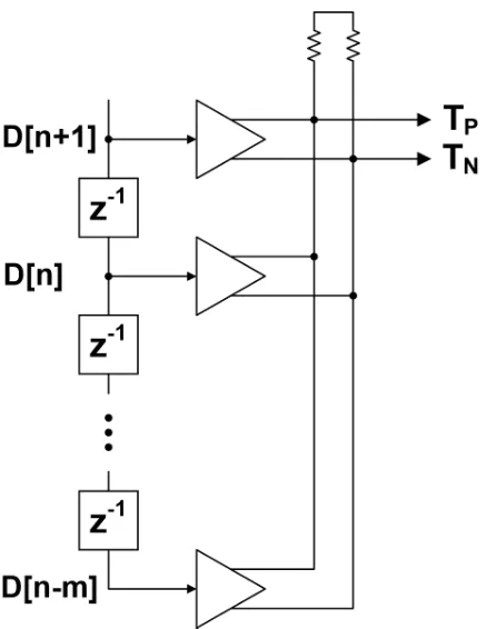
FIR-Based Pre-Emphasis. Equalization eliminates the problem of frequency-dependent attenuation by filtering the transmitted or received waveform so that the overall system exhibits a flat frequency response. For instance, in a transmitter equalizer, if the transfer characteristics of the channel is expressed by A(z), the transmitter equalization transfer function,P(z), should be designed such that A(z)×P(z) = 1 orP(z) = 1/A(z), as shown in Figure 2.18. Often times it is not possible to implement the exact required P(z); however, there are techniques to closely approximate the target transfer function. Transversal filters (FIR filters) are mainly used to perform the transmitter equalization [37]. The transfer function, H(z) can be written as
H(z) = 1 +a1z−1 +...+anz−n, (2.14)
where ai’s are called the tap coefficients and n is the total number of equalization taps. n
Figure 2.19: Block diagram of a transmitter with m-tap FIR-based equalization.
of taps in the equalizer, the better the approximation of P(z) is achieved. This technique is very well suited for digital communication techniques, in which generating a delay is very straightforward through use of latches and flip-flops as shown in Figure 2.19. Figure 2.20 illustrates how increasing the number of taps in an FIR-based transmitter reduces the pre-and post-cursor ISI. Figure 2.21 shows the improvement in the transmitted eye-diagram quality for one and two taps of transmitter equalization. As a case study, we consider a 2-tap realization in this section.
Figure 2.21: Eye diagram at the end of a lossy channel using a transmitter with no tap of FIR equalization as well as 1-tap and 2-tap of equalization.
Figure 2.23: Different high-frequency boosting configurations.
The main advantage of the continuous time equalization is that it mainly employs passive components and therefore has minimum power overhead. Figure 2.23 illustrates some circuit configurations employing inductors to perform high frequency boost. Detail analysis of these designs can be found in [38]. Passive continuous-time equalization is mainly employed in the receiver side, as will be explained in the next section, however transmitter equalization could be advantageous compared to receiver continuous equalization due to better noise performance. This is due to the fact that receiver high frequency peaking also amplifies high frequency noise where the signal strength is at its lowest, and hence degrades the overall SNR. The main drawback of this technique is the use of inductors, which inherently require large area. In the next chapter we will introduce a design that rectifies this problem.
2.2.3
Receiver
Figure 2.24: A typical electrical receiver block diagram.
Another important aspect of receiver design is the capability to compensate for the channel dispersion. We previously discussed the options for equalization at the transmitter side. However, as the data rate increases while the channel characteristics remain almost the same, the transmitter equalization becomes less than adequate for the excessive channel loss. Therefore designers have employed receiver equalization in conjunction with transmitter equalization to make high data rates possible over bandwidth limited channels. In the next section we will discuss different receiver equalization techniques.
2.2.3.1 Receiver Equalization
Receiver equalization is a powerful tool to compensate for the frequency dependent loss of the electrical channels. In this section we will introduce different techniques that are commonly employed by link designers to implement equalization at the receiver.
Decision Feedback Equalization. A common approach to remove ISI and enhance SNR is to employ decision feedback equalization (DFE). This technique helps to compensate for post-cursor ISI arising from the spread of a single pulse over time. The high level block diagram of a typical DFE is shown in Figure 2.25, [39]. The ISI from previous bits is compensated by adjusting the DFE taps: w1, ..., wn . The delay elements taking on values
Figure 2.25: Simplified block diagram of a decision feedback equalizer.
versions of previous samples are added or subtracted to the main sample by a summer at the front-end.
Figure 2.26: Loop-unrolling of the first tap of the DFE to remove the critical feedback loop.
Feed-Forward Equalization (FFE). Over the years one of the simplest and mostly used equalization techniques has been linear feed forward equalization (FFE). This technique usually involves the use of a linear transversal finite impulse response filter (FIR) as shown in figure 2.27. The FIR consists of adjustable tap coefficients w1, ..., wn and a discrete or
continuous unit delay, z−1 between each tap. The amount of delay, τ that each delay cell
represents can be as large as the bit-time [43], which is often referred as a symbol spaced equalizer. If τ < Tb the equalizer is called a fractionally spaced equalizer (FSE) [44–46].
Figure 2.27: Feed-forward equalization at the receiver.
Continuous Time Linear Equalization (CTLE). Receiver equalization can also be implemented with a continuous-time amplifier that provides a high frequency boost. Usually the transfer function of these kinds of amplifier are adjustable to accommodate different channels. These amplifiers can be employed at the receiver front-end as the pre-amplifier to not only increase the signal level reaching the slicer, but to partly compensate for the channel loss. An example of such amplifier is shown in Figure 2.28. Here, programmable RC-degeneration in the differential amplifier creates a high-pass filter transfer function which compensates the low-pass channel [48, 49].
Another example of the continuous time linear equalizer is shown in Figure 2.29(a). This passive equalizer acts as a high-pass filter to compensate for the channel loss [49]. However, it introduces loss at low frequency which degrades the SNR at the slicer input. As a result, in most applications it is followed by an amplifier to improve SNR. The linear equalizer shown in Figure 2.29(b) employs a high frequency and a low frequency path to achieve high frequency boost [50].
Figure 2.28: Continuous-time receiver equalization using frequency dependent source degeneration.
rate, particularly in time-division demultiplexing receivers. In addition, the frequency boost introduced by the CTLE also amplifies the high frequency noise and degrades SNR at the receiver. This is especially problematic at high data rates, as the received signal is weak.
2.2.4
Timing Recovery
For maximum timing margin, the receiver should sample the bits in the middle of the data eye. The performance of the link is affected by how well the clock edge is positioned with respect to the incoming data stream. This clock position must be determined from the phase and frequency of the incoming data by the timing recovery circuit. In typical high-speed links, due to the process mismatches, time variations and undefined delays in the signal path, the received data can have an undefined phase and frequency. In a communication link either a separate clock signal can be transmitted along the data signal for timing information, which is known as forwarded-clock technique, or the clock should be recovered from the incoming data signal.
In a forwarded-clock link, the transmitted clock is employed in the receiver to perform data resolution. However, the mismatch between the phase of the data and received clock can cause detection error. As a result, a phase recovery system is required to adjust the sampling clock properly for best BER performance. On the other hand, in systems with clock recovery at the receiver, both clock frequency and phase need to be adjusted at the receiver.
Figure 2.30: Clock recovery at the receiver.
adopted to define the best sampling point. The most common approach is to assume that the best sampling time is where the overall ISI is minimum. At this point the vertical eye-opening in the eye-diagram is maximum.
Figure 2.31: CDR phase detectors: (a) linear [51], (b) binary [52]
are not practical.
As shown in Figure 2.31, the phase detector can either be linear [51], which provides both sign and magnitude information of the phase error, or binary [52], which provides only phase error sign information. These phase detectors are also known as bangbang. While CDR systems with linear phase detectors are easier to analyze, generally they are harder to implement at high data rates due to the difficulty of generating narrow error pulse widths, resulting in effective dead-zones in the phase detector [54]. Bangbang phase detectors minimize this problem by providing equal delay for both data and phase information and only resolving the sign of the phase error [55].
2.2.5
Advanced Modulation Techniques
Figure 2.32: Simple binary (1bit/symbol) and PAM-4 (2bits/symbol) modulations.
data rates over band-limited channels. Multi-level pulse amplitude modulation (PAM), most commonly PAM-4, is a popular modulation scheme which has been employed in many designs [10, 56–58]. As shown in Figure 2.32, in PAM-4 modulation each symbol is comprised of two bits, which allows transmission of an equivalent amount of data in half the channel bandwidth. However, due to the transmitter’s peak-power limit, the voltage margin between symbols is 3X (9.5dB) lower with PAM-4 versus simple binary signaling. As a result, in order to benefit from the bandwidth efficiency of this modulation scheme, while not sacrificing the overall SNR the channel loss at the PAM-2 Nyquist frequency should be greater than 10dB relative to the previous octave [59]. However, this rule can be somewhat optimistic due to the differing ISI and jitter distribution present with PAM-4 signaling [24].
reduction in per-band loss and the ability to selectively avoid severe channel nulls. Typi-cally, in systems such as modems where the data rate is significantly lower than the on-chip processing frequencies, the required frequency conversion in done in the digital domain and requires DAC transmit and ADC receive front-ends [60]. While it is possible to implement high-speed transmit DACs [61], the excessive digital processing and ADC speed and precision required for multi-Gb/s channel bands results in prohibitive receiver power and complexity. Thus, for power-efficient multi-tone receivers, researchers have proposed using analog mix-ing techniques combined with integration filters and multiple-input multiple-output (MIMO) DFEs to cancel out band-to-band interference [62].
Serious challenges exist in achieving increased inter-chip communication bandwidth over electrical channels while still satisfying I/O power and density constraints. As discussed, current equalization and advanced modulation techniques allow high data rates over severely band-limited channels. However, this additional circuitry comes with a power and complexity cost. The demand for higher data rates will result in increased equalization requirements and further degrade link energy efficiencies. These issues motive investigation of novel low-power and compact equalization techniques to enable highly parallel data communication for chip-to-chip applications, which is discussed in the next section.
2.3
Summary
techniques heavily add to the complexity, power consumption and area of the transceivers. Parallelism is a natural way to achieve high aggregate data rates to meet the IO band-width requirements of the future computational and storage systems such as high perfor-mance processors and data centers. However, highly parallel links demand low power con-sumption per IO and additionally an efficient way to combat the excessive crosstalk induced from neighboring channels. Therefore, ultra low-power crosstalk cancellation techniques are necessary to allow for a high level of parallelism.
Chapter 3
High-Speed Low-Power Electrical
Transceivers
have been proposed to remove the effects of crosstalk. The design in [73] employs an FFE equalizer and [74] and [76] use crosstalk-induced jitter equalization at the transmitter and receiver, respectively. Other approaches to compensate for crosstalk noise include the use of staggered I/Os [77] or a finite-impulse response (FIR) filter at the transmitter [78–80]. All these schemes result in significant power consumption and are not suitable for parallel data links.
In this chapter, we introduce novel techniques to implement receiver and transmitter equalization as well as crosstalk cancellation in a low-power and compact manner to enable highly parallel electrical communication links that achieve high aggregate data rate as a solution to the ever increasing demand for IO bandwidth requirements. We will start with the low-power receiver architecture with far-end crosstalk cancellation and introduce a novel implementation of decision feedback equalization using a switched-capacitor (SC) technique to enable realization of many taps with better power efficiency compared to conventional techniques [83, 84]. We next elaborate on the crosstalk cancellation scheme and explain how the SC technique can be employed to implement this technique with minimal power overhead. Circuit implementation and experimental results will be discussed next.
In the second part of this chapter we introduce a transmitter equalization technique suit-able for low-power high data rate application using passive linear equalization. Adjustsuit-able equalization is performed employing controllable peaking inductors realized in a 3-D struc-ture to minimize area. We will compare this technique with the conventional FIR-based equalization and conclude this chapter with the CMOS implementation of the proposed transmitter and experimental results.
3.1
Receiver Architecture
Figure 3.1: A typical parallel communication link. Signal integrity is degraded due to channel dispersion and crosstalk noise of the neighboring channels.
at the receiver. This technique helps to compensate for post-cursor ISI arising from the spread of a single pulse over time.
Figure 3.2 shows the top level architecture of the receiver. It employs a 2-tap DFE to compensate for the post-cursor ISI. It will be shown later that this architecture can be readily generalized to n-taps of equalization. As explained in previous chapter, in the DFE, weighted versions of previous bits are added to or subtracted from the main sample by a summer at the front-end. As shown in Figure 3.2, in the 2-tap DFE, the ISI from the previous two bits is compensated by adjusting taps H1 and H2. To avoid timing issues in the first tap
equalization path, a speculative DFE architecture is employed, in which the outcomes for both possible values (one and zero) of the previous bit are fully resolved to digital levels. A multiplexer then chooses the correct value based on the resolved previous bit. Therefore, two clocked latches are required to restore the digital levels. The design employed in this paper uses a combined analog multiplexer and latch to select one of the two analog voltages directly at the output of the summer and resolve the digital bit [64]. The power consumption associated with latches is reduced since a single latch is embedded into the multiplexer, as shown in Figure 3.2.
con-Figure 3.2: Top level architecture of the proposed receiver employing half-rate clocking and loop-unrolling.
sumption [82]. This approach helps to relax the DFE timing constraint and the design requirements of the clocking and the slicers as they will be operating in a fraction of the data rate. The inherent demultiplexing enabled by this technique helps to save power in the following digital stages. Crosstalk cancellation in the proposed design is performed via a novel, low-power technique in which the aggressor signal is used to reproduce the coupling noise, as shown in Figure 3.2. Further details of this technique will be provided later in this chapter.
3.2
Decision Feedback Equalization Implementation
[image:69.612.133.490.69.350.2]where the number of summers is large.
3.2.1
Current-Mode Summers
Conventionally, taps of the equalizer are implemented using current-mode summers [11, 12, 48, 85]. Figure 3.3(a) illustrates the schematic of a current summer. The currents from each tap are set by the tap coefficienct and added at the output nodes. The resulting output will be equal to R(I1 +I2 +...+In). This configuration is quite power hungry due to its large
static current. In addition, the power consumption of the summer increases proportionally with the number of taps. The extra capacitance due to equalization taps also introduces additional loading at the summer output and limits its bandwidth. For a resistive summer, the settling time is determined largely by the load resistor and load capacitance at the output of the summer. As approximately three RC time constants are needed to achieve 5% settling accuracy, the load time constant is set such that
Tb = 3RDCL, (3.1)
where CL is the total output capacitance. As a result, assuming complete switching of the
input transistors, all the current steers into one side and the resulting voltage at the input will be equal to
VOU T =RDIt=
TbIt
3CL
, (3.2)
where I is the tail current. As can be observed from this equation, in order to maintain the output voltage while adding more equalization taps, the tail current and hence overall power consumption has to be increased.


![Figure 2.9: Transfer characteristics of typical backplane channels with and without via stubs at differentlengths [22].](https://thumb-us.123doks.com/thumbv2/123dok_us/9135286.988591/40.612.182.430.72.289/figure-transfer-characteristics-typical-backplane-channels-stubs-dierentlengths.webp)