N A N O E X P R E S S
Open Access
Performance improvement of phase-change
memory cell using AlSb
3
Te and atomic layer
deposition TiO
2
buffer layer
Sannian Song
1*, Zhitang Song
1, Cheng Peng
1, Lina Gao
2, Yifeng Gu
1, Zhonghua Zhang
1,3, Yegang Lv
1,
Dongning Yao
1, Liangcai Wu
1and Bo Liu
1Abstract
A phase change memory (PCM) cell with atomic layer deposition titanium dioxide bottom heating layer is investigated. The crystalline titanium dioxide heating layer promotes the temperature rise in the AlSb3Te layer which causes the reduction in the reset voltage compared to a conventional phase change memory cell. The improvement in thermal efficiency of the PCM cell mainly originates from the low thermal conductivity of the crystalline titanium dioxide material. Among the various thicknesses of the TiO2buffer layer, 4 nm was the most appropriate thickness that maximized the improvement with negligible sacrifice of the other device performances, such as the reset/set resistance ratio, voltage window, and endurance.
Keywords:phase change memory, atomic layer deposition, TiO2buffer layer, reset voltage, AlSb3Te
Background
Phase change memory (PCM) has been regarded as the one of the most promising nonvolatile memories for the next generation because of the advantages of high speed, low power, good endurance, high scalability, and fabrica-tion compatibility with complementary metal-oxide-semiconductor (CMOS) process [1-4]. PCM uses the reversible phase change between the crystalline and amorphous states of chalcogenide materials brought about by Joule heating. Ge2Sb2Te5 (GST) is the most widely used due to its relatively good trade-off between thermal stability and crystallization speed. However, with low crystallization temperature (around 140°C), GST is susceptible to the issue of thermal cross-talk by the proximity effect [5]. The high reset current (mA) results in high power consumption for GST-based PCM [6]. The switching speed, which is limited by its nucleation-dominated crystallization mechanism, is insufficient to satisfy the requirement of dynamic random access mem-ory (around 10 ns) is also not satisfactmem-ory [7]. These
issues stimulate us to explore novel material system in order to improve the storing media characteristics. Compared with GST, Sb-rich Sb-Te materials have many advantages such as low melting point and fast crystallization [8]. However, it is difficult to guarantee a satisfactory data-retention time at 80°C due to its relatively low crystallization temperature [9]. Recently, the Al-Sb-Te (AST) ternary system has been proposed for application in electric memory [10,11]. Compared with GST, Al-Sb-Te exhibits a high crystallization temperature, good data re-tention, and high switching speed.
It was reported that merely 0.2% to 1.4% of the total applied energy is effectively used for phase changing, and nearly 60% to 70% of the energy transfers back along the columnar tungsten (W) bottom electrode, hav-ing not participated in the heathav-ing process of the phase change material (for a T-shaped PCM cell) [12]. Such a low thermal efficiency inevitably leads to a large operat-ing bias/current duroperat-ing the phase change processes. Consequently, one of the effective solutions that has been tried to enhance the thermal efficiency is using an appropriate heating layer between the phase change ma-terial layer and the underlying W electrode, or replacing the W plug with some other suitable material. There are some qualified materials that have already been applied
* Correspondence:[email protected]
1State Key Laboratory of Functional Materials for Informatics, Shanghai
Institute of Micro-system and Information Technology, Chinese Academy of Sciences, 865 Changning Road, Shanghai 200050, China
Full list of author information is available at the end of the article
thinner TiO2film. The electrical resistivity of a crystal-line TiO2film measured by the van der Pauw method in this study is about 1.2Ωcm, which is close to the result reported by Xu et al. [17]. In addition, TiO2 has a high melting point (approximately 2116 K) and will be ther-mally stable under high temperature (approximately 900 K) during the reset operation. Generally speaking, with the suitable electrical resistivity, thermal conductiv-ity and thermal stabilconductiv-ity, a crystalline TiO2layer should hopefully serve as the bottom heating layer in PCM cells to improve the thermal efficiency and, therefore, reduce the power requirement during phase transitions. In this study, the atomic layer deposition (ALD) TiO2was used as a buffer layer which was expected to improve the thermal efficiency and reduce the reset voltage of PCM.
Methods
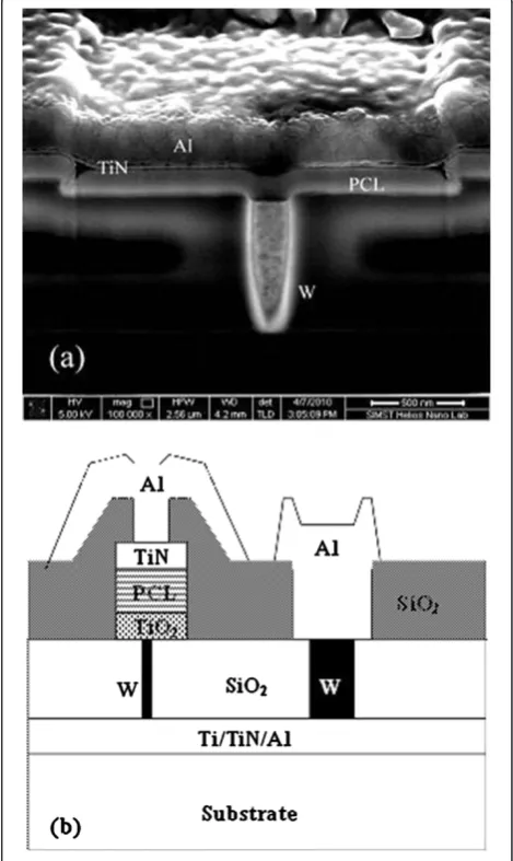
The PCM cells in this study are fabricated using 0.18
μm CMOS technology. Figure 1a shows a cross-section transmission electron microscopy (TEM) image of the fabricated cell without TiO2 buffer layer. The diameter and height of the columnar W electrode are 260 and 700 nm, respectively. Figure 1b shows a schematic dia-gram of the cross-section structure of the fabricated cell with TiO2 buffer layer. The thin TiO2 layer was interposed between the phase change layer (PCL) and W plug. A 2-, 4-, and 8-nm thick TiO2 buffer layer was deposited by ALD at 400°C using Beneq TFS 500 ALD system (Beneq, Vantaa, Finland). One deposition cycle was composed of Ti precursor (TiCl4) pulse (250 ms), 200 sccm N2 purge (2 s), water (H2O) pulse (250 ms), and 200 sccm N2 purge (s2 s). The deposition rate is 0.5 A/cycle. The as-deposited films were crystallized with rutile structure measured by X-ray diffraction. Then, 100-nm thick AST PCL was deposited by magne-tron sputtering. The background pressure and Ar gas pressure were 2.0 × 10⁻⁴ and 0.18 Pa, respectively. The stoichiometry of the deposited films was confirmed by electron dispersive spectroscopy. The Al/Sb/Te ratio was 1:3:1. Then, 20 nm TiN and 200 nm Al were deposited by sputtering as top electrode. For comparison, sputter-deposited AST film without the interposed TiO2layer was
also fabricated with the same structure. The electric pro-perty tests of PCM were carried out by a Tektronix AWG5012b arbitrary waveform generator (Tektronix, Inc., Shanghai, China) and a Keithley 2602A parameter analyzer (Keithley Instruments, Inc., OH, USA).
Results and discussion
[image:2.595.304.539.93.487.2]Figure 2a shows the sheet resistance change of AST films as a function of temperature. The sample with a thickness of 100 nm was prepared on the SiO2/Si(100) by sputtering at room temperature. Upon heating, the sheet resistance of AST films decreased with a rapid drop at the crystallization temperature (Tc). The Tc, defined by the temperature corresponding to minimum of the first derivative of R-T curve, was about 198°C which is higher than that of GST films (approximately
Figure 1Cross-sectional structures of PCM cells.(a) Cross-sectional structure of PCM cell without TiO2buffer layer and (b)
145°C) [22]. To check the crystallization kinetics, electrical resistivity was in situ measured with increasing temperature with various heating rates dT/dt. Applying Kissinger’s analysis which relates the transition temperatureTc, the rate of heating (dT/dt), and the activa-tion energy (Ea) for crystallization by the formula below:
lnðdT=dtÞ=Tc2
¼CðEa=kBTcÞ; ð1Þ
whereCis a constant,kBis the Boltzmann constant, a plot of ln[(dT/dt)/Tc2] against 1/Tc yields a straight line with slope,−Ea/kB. From the Kissinger plot shown in Figure 2b, the activation energy for crystallization of AST was determined to be about 3.55 eV which is higher than that of GST films (approximately 2.01 eV) [22]. It has to be noted that the high crystallization temperature and high activation energy of AST offer a large benefit for a stable operation of the PCM device because the cells in the amorphous state tend to switch to the crystalline state due to cross talk, i.e., the heat dissipation from other cells.
The bright-field TEM was used to study the structure of thin films. Figure 3 shows the TEM image of AST film after a 2-min heating at 400°C in Ar atmosphere; nanocrystals (dark spots) were observed. Peng et al. reported that an embedded crystal structure of hex-agonal (Sb2Te) and monoclinic (Al2Te3) phases can be found in AST materials [10]. The black area in the image results from an overlap of Sb2Te and Al2Te3 crys-talline grains. The overlap of grains will lead to a larger local density, and the incident electrons will be more scattered by these areas.
The phase transition of PCM cell can be characterized from the relation between the cell resistance and the corresponding amplitude of voltage pulse or current pulse (so called R-V or R-I curve). The measured R-V
curves for AST PCM cells with different pulse width are shown in Figure 4a. Reversible phase-change process has been observed. As revealed, once the programming
voltage increases beyond the threshold voltage, the cell resistance starts to drop due to the crystallization of AST alloy and then reaches a minimum, which is corresponding to the set resistance. When the voltage is further increased, the resistance again rises and then returns to the reset state. It is clear that the set resist-ance decreases with the pulse width. The higher set re-sistance resulted from a shorter pulse implies that incomplete crystallization states are formed after set programming. It can be seen from Figure 4a the resist-ance of the AST devices dramatically increased by two orders of magnitude at a reset voltage of around 4.1 V (at 50 ns).
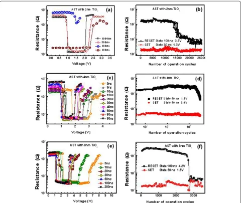
[image:3.595.58.540.89.235.2]Figure 5a,c,e shows the variations in cell resistance with the 2-, 4-, and 8-nm thick TiO2 buffer layer as a function of the voltage for the set and reset operations, respectively. For the device with 2 nm TiO2, as shown in Figure 5a, a 100-ns width pulse fails to set the cell and a pulse width of 100 ns is insufficient for a complete reset programming, suggesting that 2 nm TiO2 layer indeed leads to a slower crystallization process, thus longer write time for the set operation. For a device with 8 nm TiO2, as shown in Figure 5e, a 5-ns pulse can trigger re-versible phase-change of the cell, and the reset voltage of approximately 3.8 V (at 50 ns) of the cell is clearly lower than that of the AST cells (about 4.1 V) without TiO2layer. With 50-ns, pulse reset voltage of 2.4 V was achieved for the device with 4 nmTiO2layer (in Figure 5c), which is only about half of the voltage required by the de-vice without TiO2 buffer layer. The voltage reduction could be understood from the high Joule heating efficiency and the good thermal confinement. The oxide interfacial layer prevents heat generated in the programming volume of the AST from diffusing to the plug, which has high thermal conductivity, resulting in low power set/reset op-eration. Similar improvement has been reported on other kinds of oxide interfacial heater layers [23,24]. Besides that, both of the resistances in amorphous and crystalline
states retained at the same levels after inserting the TiO2 layer. These results prove a fact that the inserted TiO2 layer will not drift the resistance but can sharply diminish the operation voltage, which will be helpful to solve the difficult problem in the compatibility with the continuing scaling down dimension in CMOS process. It is worthy to point out that the set resistance is very stable for the cells with TiO2layer at different pulse widths, suggesting that the TiO2layer helps to raise the temperature profile within the phase change film and, thereby, enhances the heat-induced phase transition process. Furthermore, there are some other advantages of TiO2such as easily fabricated,
no pollution, fully compatible with CMOS process, and avoids the diffusion between phase change material and bottom electrode.
[image:4.595.59.540.88.386.2]Figure 4b and Figure 5b,d,e show the repeatable resist-ance switching between the set and reset states of the cells without and with TiO2 layer, respectively. For the device without TiO2, as shown in Figure 4b, the endur-ance capability keeps about 20,000 cycles before the presence of resistance disorder with a set stuck failure mechanism. For the device with 2 nm TiO2, as shown in Figure 5b, the reset resistance reduced gradually during the cycling. After 14,000 cycles, the reset resistance
Figure 4Resistance voltage and endurance characteristics.(a) Resistance voltage characteristics of PCM cell with AST films by different voltage pulse widths. (b) Endurance characteristics of the PCM cell with AST film.
[image:4.595.60.540.575.705.2]dropped rapidly, leading to the endurance failure by losing the set and reset resistance window. For the device with 8 nm TiO2, as shown in Figure 5f, the endurance capabi-lity keeps about 2,700 cycles before the presence of resis-tance disorder with a reset stuck failure mechanism. Good endurance characteristics (>104cycles) was found in the cell with 4-nm TiO2buffer layer. The low resistance state maintained around 103Ωmagnitude, and the high resis-tance state kept on 105 Ω level, indicating a satisfactory data resolution capability for random access memory ap-plication. The difference cyclic operation behavior shown in Figure 4b and Figure 5b,d,e suggested the different per-formance degradation processes for the device with and without TiO2layer, which is currently under investigation. Among the various thicknesses of the TiO2buffer layer, 4 nm was the most appropriate thickness that maximized
the improvement with negligible sacrifice of the other de-vice performances, such as the reset/set resistance ratio, voltage window, and endurance.
Conclusions
[image:5.595.58.539.88.493.2]This paper reports an efficient method for reducing the reset voltage and power of the conventional T-shaped PCRAM, which has the potential to replace the current nonvolatile memories. We inserted TiO2 layer between phase change memory and bottom electrode to increase the utilization of the Joule heat and reduce the heat dis-sipation. Due to the suitable electrical resistivity and the low thermal conductivity of TiO2film, the overall set re-sistance of the PCM cell will not be greatly increased, while the remarkably increased overall thermal resist-ance helps to reduce the reset voltage.
Figure 5Resistance voltage characteristics of PCM cell at different pulse widths.(a) 2, (c) 4, and (e) 8 nm TiO2. Endurance characteristics of
Acknowledgments
This work was supported by the National Key Basic Research Program of China (2010CB934300, 2011CB9328004, and 2011CBA00607), the National Integrate Circuit Research Program of China (2009ZX02023-003), the National Natural Science Foundation of China (61006087, 61076121, 61176122, and 61106001), the Science and Technology Council of Shanghai (11DZ2261000 and 1052nm07000), and the Chinese Academy of Sciences (20110490761).
Author details
1State Key Laboratory of Functional Materials for Informatics, Shanghai
Institute of Micro-system and Information Technology, Chinese Academy of Sciences, 865 Changning Road, Shanghai 200050, China.2Division of Nuclear
Materials Science and Engineering, Shanghai Institute of Applied Physics, Chinese Academy of Sciences, 2019 Jialuo Road, Jiading District, Shanghai 201800, China.3National Laboratory for Infrared Physics, Shanghai Institute of
Technical Physics, Chinese Academy of Sciences, Shanghai 200083, China.
Received: 16 November 2012 Accepted: 30 December 2012 Published: 15 February 2013
References
1. Ovshinsky SR:Reversible electrical switching phenomena in disordered structures.Phys Rev Lett1968,21:1450–1453.
2. Wuttig M, Yamada N:Phase-change materials for rewriteable data storage.Nat Mater2007,6:824–832.
3. Kolobov AV, Fons P, Frenkel AI, Ankudinov AL, Tominaga J, Uruga T:
Understanding the phase-change mechanism of rewritable optical media.Nat Mater2004,3:703–708.
4. Lai S:Current status of the phase change memory and its future. In
Electron Devices Meeting: December 8–10 2003, Santa Clara. New York: IEEE; 2003:10.1.1–10.1.4.
5. Kao KF, Chang CC, Chen FT, Tsai MJ, Chin TS:Antimony alloys for phase-change memory with high thermal stability.Scr Mater2010,63:855–858. 6. Jung Y, Agarwal R, Yang CY, Agarwal R:Chalcogenide phase-change
memory nanotubes for lower writing current operation.Nanotechnology
2011,22:254012.
7. Wong HSP, Raoux S, Kim S, Liang JL, Reifenberg JP, Rajendran B, Asheghi M, Goodson KE:Phase change memory.Proc IEEE2010,98:2201–2227. 8. Lee ML, Miao XS, Ting LH, Shi LP:Ultrafast crystallization and thermal
stability of In-Ge doped eutectic Sb70Te30phase change material.
J Appl Phys2008,103:043501.
9. Wang F, Zhang T, Song ZT, Liu C, Wu LC, Liu B, Feng SL, Chen B:
Temperature influence on electrical properties of Sb-Te phase-change material.Jpn J Appl Phys2008,47:843–846.
10. Peng C, Song ZT, Rao F, Wu LC, Zhu M, Song HJ, Liu B, Zhou XL, Yao DN, Yang PX, Chu JH:Al1.3Sb3Te material for phase change memory application.Appl Phys Lett2011,99:043105.
11. Ren K, Rao F, Song ZT, Lv SL, Cheng Y, Wu LC, Peng C, Zhou XL, Xia MJ, Liu B, Feng SL:Pseudobinary Al2Te3-Sb2Te3material for high speed phase
change memory application.Appl Phys Lett2012,100:052105. 12. Sadeghipour SM, Pileggi L, Asheghi M:Phase change random access
memory, thermal analysis. InThe Tenth Intersociety Conference on Thermal and Thermomechanical Phenomena and Emerging Technologies in Electronic Systems, ITherm 2006: May 30–June 2 206; San Diego, California. New York: IEEE; 2006:660–665.
17. Xu C, Song ZT, Liu B, Feng SL, Chen B:Lower current operation of phase change memory cell with a thin TiO2layer.Appl Phys Lett2008,
92:062103.
18. Cheng HY, Chen YC, Lee CM, Chung RJ, Chin TS:Thermal stability and electrical resistivity of SiTaNxheating layer for phase-change memories. J Electrochem Soc2006,153:685–691.
19. Kim C, Suh DS, Kim KHP, Kang YS, Lee TY, Khang Y, Cahill DG:Fullerene thermal insulation for phase change memory.Appl Phys Lett2008,
92:013109.
20. Rao F, Song ZT, Gong YF, Wu LC, Feng SL, Chen B:Programming voltage reduction in phase change memory cells with tungsten trioxide bottom heating layer/electrode.Nanotechnology2008,19:445706.
21. Mun J, Kim SW, Kato R, Hatta I, Lee SH, Kang KH:Measurement of the thermal conductivity of TiO2thin films by using the thermo-reflectance
method.Thermochim Acta2007,455:55–59.
22. Song SN, Song ZT, Liu B, Wu LC, Feng SL:Stress reduction and performance improvement of phase change memory cell by using Ge2Sb2Te5–TaOxcomposite films.J Appl Phys2011,109:034503. 23. Rao F, Song ZT, Gong YF, Wu LC, Liu B, Feng SL, Chen B:Phase change
memory cell using tungsten trioxide bottom heating layer.Appl Phys Lett
2008,92:223507.
24. Li MH, Zhao R, Law LT, Lim KG, Shi LP:TiWOxinterfacial layer for current reduction and cyclability enhancement of phase change memory. Appl Phys Lett2012,101:073502.
doi:10.1186/1556-276X-8-77
Cite this article as:Songet al.:Performance improvement of
phase-change memory cell using AlSb3Te and atomic layer deposition TiO2
buffer layer.Nanoscale Research Letters20138:77.
Submit your manuscript to a
journal and benefi t from:
7Convenient online submission 7Rigorous peer review
7Immediate publication on acceptance 7Open access: articles freely available online 7High visibility within the fi eld
7Retaining the copyright to your article