Abstract
It was reported that during silicon etching, silver was subjected to have a controversial role. Some researchers debate that silver protects silicon, and, at the same time, other ones confirm that silver catalyzes silicon underneath. In this paper, we give experimental results arguing the dual role that silver has during the formation of silicon nanostructures. We give a proof that the role of silver depends on the experimental details and the intrinsic properties of silver during its deposition on the silicon wafer. Through our investigations, we tracked the silver particles that indicated which mechanism is involved. Characterizations of the prepared samples were made using a scanning electron microscope.
Keywords:Silicon nanowires, Silver, HF, Etching, Catalyzing
Background
By etching silicon in a HF aqueous solution, porous sili-con can be formed. When silisili-con etching in the HF so-lution is assisted by silver, well-organized nanostructures like silicon nanowires [1-3] are formed. The latter are very interesting in electronic and photovoltaic applica-tion. In order to enable significant improvements in the devices’ technologies, understanding of the fabrication mechanism must be attained to produce materials with precise control. Herein, we are interested in the silver-assisted chemical etching of silicon in HF solution. This technique can be realized either by a one-step process or a two-step process. The one-step method includes, at the same time, metal deposition and electroless etching. In this process, the silicon substrate is immersed in an AgNO3/HF aqueous solution. The two-step method con-sists first of metal deposition and second, the chemical etching. In the latter method, the silver particles are eva-porated or chemically formed on the surface of the silicon sample then introduced in a HF aqueous solu-tion. With these two processes, we obtain two different behaviors of the silver particles; in one case, the silver catalyzes silicon, and in the other one, it protects the silicon underneath. Therefore, using a scanning electron
microscopic (SEM) characterization, we tracked silver particles during silicon etching to determine which mechanism is privileged. To interpret the obtained results, we analyze charge displacement at the metal/Si interface. The developed model clarifies the role that the silver has during silicon metal-assisted etching experi-ences. Hence, the controversy regarding this role is solved.
Methods
For cleaning, samples were boiled in acetone for 10 min, followed by their immersion in ethanol for 5 min to re-move organic greases. Then, we rinsed them three times with deionized water. Finally, samples were dipped in a 5% aqueous HF solution for 1 min to eliminate native silicon dioxide. This study was realized at two ambient conditions: room temperature and atmospheric pressure. The etching duration was 1 h. We used high purity single-crystalline silicon. The wafers are p-type, boron-doped and (100)-oriented, with a thickness of 525 μm and a resistivity of 1 to 10Ωcm. The samples were then separated in sample A and sample B to be treated differ-ently. Sample A was immersed in an etching solution
composed of HF/AgNO3 [1-3]. The concentrations in
the latter were 40% and 0.02 M, respectively. On sample B, we first evaporated a 30-nm silver film, and then it was immersed in a 40% HF aqueous solution [4]. * Correspondence:[email protected]
Laboratoire de Photovoltaique, Centre de Recherches et des Technologies de l’Energie, Technopole de Borj-Cedria, BP 95, Hammam-Lif, Tunis 2050, Tunisia
Our SEM observations show two different structures; in the case of the one-step process (sample A), we obtained silicon nanowires (SiNWs) covered with a den-dritic silver film. We did not observe any silver nanopar-ticle at the bottom of SiNWs. In the two-step process (sample B), we obtained silicon pores. However, Fang et al. [4] obtained SiNWs by etching a silicon wafer on which they evaporated a 20-nm silver film.
Results and discussion
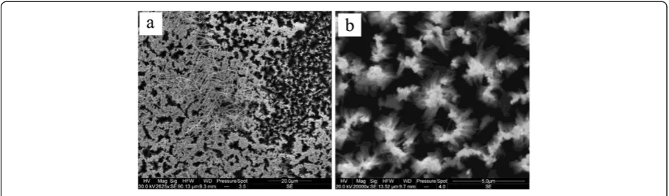
In Figure 1, we give the top section SEM images of sam-ple A, where the silver nanoparticles cover the top sur-face of the SiNWs. The silver film formed on wafer A is not uniform and not compact. The nonhomogeneity of this film can be attributed to the surface status. It was reported in several works [5-7] that the dendrites forma-tion is related to the electrons’exchange between silicon atoms and silver ions. In Figure 1a, we observe in some regions silver nanoparticles on top of SiNWs, where the image in Figure 1b is the magnification of this zone. In other regions, the silver forms a filament-like structure. The growth mechanism of silver dendrites is still un-clear; the diffusion-limited aggregation theory [8] may play an important role to explain this mechanism. We
notice that we did not see any silver nanoparticles at the bottom of SiNWs.
However, in the case of sample B, where a 30-nm sil-ver film was deposited before the etching step, we ob-serve pores formation at a depth of 200μm as shown in Figure 2. Figure 2a is a tilted SEM image of the sample showing both the top surface and the cross section. We notice the beginning of pores from the top of the wafer and the presence of silver nanoparticles in the bottom of pores which is magnified in image (Figure 2b). The formed pores are not uniform. Hence, we observe the pores at different depths. The average of the pore dia-meters is around several microdia-meters. This could be due to the thickness of the silver film.
From the obtained results for samples A and B, we esti-mate the etching rate for sample A at about 0.5 μm/min and the penetration rate of silver particles for sample B at about 2.7μm/min.
[image:2.595.56.540.89.231.2]In this work, we aim to explain the mechanism gov-erning silicon etching to obtain SiNWs or pores. In the two metal-assisted etching structures, the intrinsic prop-erties of the metal orientate the silicon etching. The lat-ter is initiated by the formation of silicon dioxide. It was reported [9] that silver-assisted etching of silicon, in Figure 1SEM images of sample A.(a) silver dendrites and nanoparticles and (b) magnification of silver nanoparticles.
Silver nanoparticles
[image:2.595.57.545.555.715.2]b
a
presence of H2O2, leads to a homogenous and large film SiNWs. In addition, the etching reaction is 250 times lower in absence of H2O2 [9]. However, as obtained in the present work and reported by Peng et al. [1], SiNWs could be also obtained without H2O2. In the used solu-tion in this work, there are many oxidizing agents, and
the most important one is the (NO3)− ions. The
SiO2þ6 HF!H2SiF6þ2 H2O ð5Þ
The electroless metal deposition mechanism was pre-sented by Morinaga et al. with copper particles [10]. Then Peng et al. started with the protecting mechanism that silver has during the silicon etching in the one-step method [1]. After that, they provided in [11] their new position regarding the etching processes of silicon wafers in aqueous HF/AgNO3solution where the catalyzing ef-fect was described. Qiu et al. [12] gave experimental evi-dences that silver protects the silicon underneath. Consequently, the role that silver has was still not elucidated.
[image:3.595.56.292.89.258.2] [image:3.595.56.292.326.398.2]In this section, we give the explanation of SEM images in Figures 1 and 2. Therefore, to understand the etching process of samples A and B, we propose a unique inter-pretation of the experimental observations in both cases by analyzing what happens at the silver/silicon interface. In Figure 3, we give the schematic band structure at the silver/silicon interface. In such a case, the work function of silver (ϕAg= 4.3 eV) is less than that one of silicon (ϕSi= 4.9 eV). Consequently, at contact, electrons diffuse from the metal to the semiconductor until the thermo-dynamic equilibrium is reached at the same Fermi level. Figure 3Schematic band diagram at the Ag/Si interface.
Table 1 Values of electronegativity of Ag, Si, O, and B [13]
Elements Electronegativity
Ag 1.93
Si 1.90
O 3.44
B 2.04
A)
B)
+ + + +
c)
e-Difficult
oxidized sites a)
Si HF/AgNO3
Solution
+ + + +
e-b)
H2SiF6
+ + + +
e-Easily oxidized
sites
+ + + +
Ag c)
b)
H2SiF6
+ + + +
Ag Easily oxidized
sites
+ + + +
Ag a)
Si HF Solution
Difficult oxidized sites
Ag+ Ag+ Ag+
e-Leading to
[image:3.595.57.540.505.714.2]Leading to
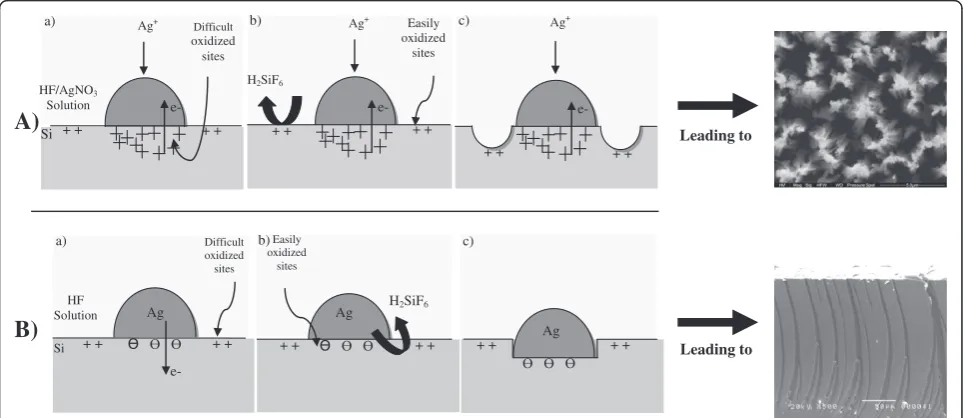
The scheme in Figure 3 explains the Ag/Si interface in the case of evaporation (sample B). However, using work functions of Ag and Si becomes impossible when the sil-ver is at its ionic form. This is related to the fact that the work function of a metal is defined as being the needed energy to extract one electron from its metallic con-ductor. Unfortunately, this is not applicable in the case of silver ions when they capture electrons from silicon. In such a case, we have to use electronegativity which is the aptitude of an element to attract electrons. In Table 1, we give values of the electronegativity of Ag, Si, O, and B (boron) elements involved in the etching mechanism. The electronegativity of the silver ion is greater than that of silicon. The electrons move from silicon to silver ions. At contact, the silicon underneath the silver particles becomes more positively doped than the silicon around silver.
The aptitude of oxidizing silicon depends on the sili-con status; from values in Table 1, we can deduce that oxidizing pure silicon substrate (intrinsic silicon) is easier than oxidizing pure boron material. We can extrapolate that boron-doped silicon has an effective electronegativity value ranging between 1.90 (Pure Si) and 2.04 (Pure B). Consequently, in the case of sample A where silver ions are deposited on the Si substrate, there is transfer of electrons from Si to silver. Therefore, the region underneath silver becomes poor in electrons as compared to the region around silver nanoparticles. Hence, oxidizing Si around silver particles (P-doped Si) becomes more important than the Si underneath it, which behaves like P++-doped Si. Thus, the etching of oxidized sites around silver particles starts leading to the formation of SiNWs (Figure 4A, processes a-c). How-ever, in the case of sample B, due to the neutral region formed underneath the evaporated silver nanoparticles, Si around them (P-doped Si) is a difficult oxidized region as compared to Si underneath them that behaves like intrin-sic Si. As a result, etching starts underneath Ag particles leading to pores formation (Figure 4B, processes a-c).
To confirm the above mechanisms, we use twin sam-ples (sample C). After cleaning, samsam-ples were immersed
for a short duration (3 min) in a HF/AgNO3 solution
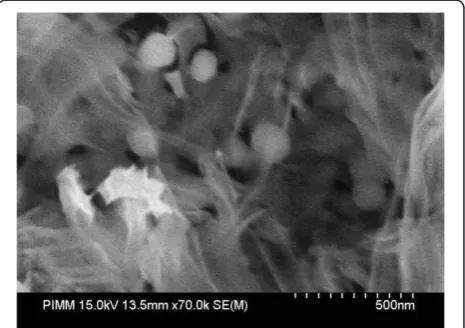
with the same concentrations used for sample A. In Fig-ure 5, we show a top SEM image of one sample where we observe silver nanoparticles deposited in the HF/ AgNO3 (image a). However, image b is a cross-section SEM view of the second sample after removing the silver film, where we observe the beginning of silicon etching. Then, the sample C with silver nanoparticles was immersed in a 40% HF aqueous solution, as done for sample B, for 2 min. Figure 6 is a SEM image of this sample after etching, where we observe silver nanoparti-cles in the bottom of etched silicon.
According to our assumptions on the role of silver during the silicon etching, the one-step process starts
during the 3 min in the HF/AgNO3solution. The
two-step process starts when the sample is immersed in sole aqueous HF solution, since silver nanoparticles are
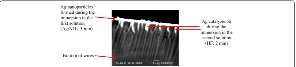
deposited in the HF/AgNO3 solution. In Figure 7, we
[image:4.595.62.539.90.213.2] [image:4.595.306.539.537.701.2]give the cross-section SEM image of sample C (with sil-ver nanoparticles) where we can see that no silsil-ver nano-particles are found in the bottom of pores. However, the Ag nanoparticles are found on the top (white color) which confirms the one-step process. In addition, it is Figure 5Top and cross-section SEM images of sample C (a) chemically deposited Ag film and (b) after removing the Ag film.
clear in our observation that silver nanoparticles start their catalyzing effect (the two-step mechanism) by dig-ging silicon at depths of 1–2μm.
Conclusions
During metal-assisted etching experiences, some
researchers reported that silver protects silicon. How-ever, others confirmed that silver catalyzes the silicon underneath. In this paper, we give experimental results arguing the dual role that silver has during silicon etch-ing. We propose a model based on the effect of electron transfer at the silver/silicon interface when silver is deposited during the HF etching (one-step method) and when silver is deposited prior to the etching in a HF so-lution (two-step method). By the proposed model, it becomes clear how silver nanoparticles can protect the silicon underneath in some experimental conditions and how they initiate pore formation by etching silicon under-neath in others.
Competing interests
The authors declare that they have no competing interests.
Authors’contributions
MAL prepared samples, performed the SEM imaging, and proposed the mechanisms of silicon etching. She also wrote the manuscript. NN helped on the SEM investigations. MB supervised the work, improved the proposed mechanisms and the text. All authors read and approved the final manuscript.
Acknowledgements
Authors are grateful to the Mitsubishi Corporation for the financial support in the form of a scholarship of 10 months, via a memorandum with the Ecopark of Science and Technology of Borj-Cedria, Tunisia.
Received: 25 April 2012 Accepted: 23 July 2012 Published: 13 August 2012
References
1. Peng KQ, Yan YJ, Gao SP, Zhu J:Synthesis of large area silicon nanowire arrays via self-assembling nanoelectrochemistry.Adv Mater2002,14:1164. 2. Peng KQ, Wu Y, Fang H, Zhong XY, Xu Y, Zhu J:Uniform, axial-orientation
alignment of one dimensional single-crystal silicon nanostructure arrays.
Angew Chem Int Ed2005,44:2737.
3. Nafie NN, Abouda Lachiheb MM, Dimassi WW, Bouaicha MM:Effect of etching time on morphological, optical, and electronic properties of silicon nanowires.Nanoscale Res Lett2012,7:393.
4. Fang H, Wu Y, Zhao J, Zhu J:Silver catalysis in the fabrication of silicon nanowire arrays.Nanotechnology2006,17:3768–3774.
5. Qiu T, Chu PK:Self-selective electroless plating: an approach for fabrication of functional 1D nanomaterials.Materials Science and
Engineering R2008,61:59–77.
6. Peng KQ, Zhu J:Morphological selection of electroless metal deposits on silicon in aqueous fluoride solution.Electrochim Acta2004,49:2563. 7. Peng KQ, Xu Y, Wu Y, Yan YJ, Lee ST, Zhu J:Aligned single-crystalline Si
nanowire arrays for photovoltaic applications.Small2005,1(11):1062. 8. Wittman TA, Sander LM:Diffusion-limited aggregation, a kinetic critical
phenomenon.Phys Rev Lett1981,47:1400.
9. Chartier C, Bastide S, Lévy-Clément C:Metal-assisted chemical etching of silicon in HF-H2O2.Electrochim Acta2008,53:5509–5516.
10. Morinaga H, Suyama M, Ohmi T:Mechanism of metallic particle growth and metal-induced pitting on Si wafer surface in wet chemical processing.J Electrochem Soc1994,14(1):2834.
11. Peng K, Fang H, Hu J, Wu Y, Zhu J, Yan Y, Lee ST:Metal-particle-induced, highly localized site-specific etching of Si and formation of single-crystalline Si nanowires in aqueous fluoride solution.Chem2006,12:7942. 12. Qiu T, Wu XL, Yang X, Huang GS, Zhang ZY:Self-assembled growth and
optical emission of silver-capped silicon nanowires.Appl Phys Lett2004, 84:3867.
13. Cheng CS, Hinshaw BC, Panzica RP, Townsend LB:Synthesis of 2-amino-5-cyano-7-(beta-D-ribofuranosyl)-pyrrolo[2,3-d]pyrimidin-4-one.An important precursor for the synthesis of nucleoside Q and Q. J Am Chem Soc 1976,98(24):7870–7872.
doi:10.1186/1556-276X-7-455
Cite this article as:Abouda-Lachihebet al.:The dual role of silver during
silicon etching in HF solution.Nanoscale Research Letters20127:455.
Submit your manuscript to a
journal and benefi t from:
7Convenient online submission
7Rigorous peer review
7Immediate publication on acceptance
7Open access: articles freely available online
7High visibility within the fi eld
7Retaining the copyright to your article
[image:5.595.57.541.89.199.2]