© 2018, IRJET | Impact Factor value: 6.171 | ISO 9001:2008 Certified Journal | Page 1190
Mollification Parameter Control By Dynamic Voltage Restorer (DVR)
Sunny Dhoke
1, Roshan Mohabe
2, Dhiraj Satkar
3, Nagmanaj Pathan
41,2,3 Student, Dept. of Electrical Engineering, W.C.E.M. Nagpur, Maharashtra, India 4Professor, Dept. of Electrical Engineering, W.C.E.M. Nagpur, Maharashtra, India
---***---Abstract -
For electrical engineering, the noteworthy topic is power quality. Power quality problem is an occurrence demonstrated as a nonstandard current, voltage or frequency. Electrical failures and service disruption can be found in utility distribution networks, detracting commercial operation and sensitive industrial loads which causes heavy financial losses. Voltage sag is one of the major problems that will be dealt here.Dynamic Voltage Restorer is a series connected device based on power electronics which can quickly mollify the voltage sag in the system and restore the load voltage to the pre-fault value.
Mollification of the power quality problem is made possible by the increasing development in power electronics. This work focuses on the major problem of voltage sag. Voltage sag problems are mollified by devices such as UPFC, tap changing transformer, STATCOM and DVR. Between these devices dynamic voltage restorer provides the most economical and commercial answer to mollify voltage sag by injecting power as well as voltage into the system. This thesis gives an introduction to significant power quality problems for DVR and power electronics controllers for voltage sag mollification. Then operation hardware and elements in DVR is explained.
This thesis gives the idea of using of the error signal to control the triggering of the switches of an inverter using Sinusoidal Pulse Width Modulation (SPWM) technique.
Key Words: Static Series Compensator (SSC), Dynamic
Voltage Restorer (DVR), Mollification, Peripheral Interface Controller (PIC).
1. INTRODUCTION
The typical power quality disturbances are voltage sags, voltage swells, intermission, phase shifts, harmonics and transients. Among the interference, voltage sag is considered the most severe since the sensitive loads are very impressionable to temporary changes in the voltage.
“Authenticity” is a key word for utilities and their customers in general, and it is very important to companies operating in a highly competitive business environment, it affects profitability and also is a driving force in the industry. A very high level of authenticity has been reached by the electrical transmission and distribution systems, there cannot be any disturbances that can be avoided. Problems related with operation of electrical and electronic devices can be caused by any disturbances to voltage. There is a need
of constant frequency, constant sine wave shape and symmetrical voltage with a constant peak to peak value to continue the production.
The wide area solution is required to alleviate voltage sags and improve power quality. One of the newest approach is using a DVR . The basic operational principle is injecting the missing voltage in series to the bus and detecting the voltage sag by zero crossing detector. DVR has become a cost effective solution for the protection of non-linear loads from voltage sags. The DVR is efficient, quick and flexible solution to voltage sag problems. DVR consists of capacitor bank storage unit, PWM inverter, and filter and booster transformer.
It is well known that power quality is facing various difficulties such as voltage sags/swells, flicker, surge, voltage imbalance, harmonic distortion and interruptions, fretting fatigue. Voltage sags/swells can occur more regularly than other power quality problems, also these sags/swells are the most serious power quality disturbances in the power distribution system. Dynamic Voltage Restorer (DVR) is one of the most important custom power devices that have been created to improve the performance of power quality. The DVR balances the load voltage at a nominal magnitude and phase by settling the voltage sag/swell. These systems can compensate voltage sags by increasing the appropriate voltages in cascade with the supply voltage, and therefore prevent loss of power.
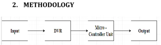
[image:1.595.307.565.521.593.2]2. METHODOLOGY
Fig -1: Block diagram of the role of dynamic voltage restorer in improving power quality.
2.1.1 Basic Configuration:
Some of the basic elements of a DVR are as follows:
Converter
L&C filter
Booster transformer DC-link and paper capacitor storage unit
DC-link and energy storage
By-pass equipment
© 2018, IRJET | Impact Factor value: 6.171 | ISO 9001:2008 Certified Journal | Page 1191 The converter is most likely a Voltage Source Converter
(VSC), which sinusoidal Pulse Width modulates (SPWM) the DC from the DC-link/storage to AC-voltages injected into the system. A VSC is a power electronic system, which consists of capacitor storage and switching devices, which can generated a sinusoidal voltage at required constant frequency, magnitude, and phase angle. In the DVR application, the VSC is used to transitory replace the supply voltage or to generate the part of the supply voltage which is missing. There are four main types of switching devices: Light Activated Silicon Controlled Rectifier (LA-SCR), Gate Turn-Off thyristor (GTO), Power Metal Oxide Semiconductor Field Effect Transistors (P-MOSFET), Integrated Gate Commutated Thyristor (IGCT) and Insulated Gate Bipolar Transistors (IGBT). Each type of power electronic device has its own advantages and limitation. The IGCT is a newly compact device which is having authenticity and enhanced performance that allows VSC to build with very large power ratings. Because of the highly practiced converter design with IGCTs, the DVR can balance dips which are above the capability of the past DVRs using conventional devices. The purpose of such devices is to supply the necessary energy to the VSC using a dc link for the generation of injected voltages.
2.1.2 L&C Filter:
To reduce the switching harmonics generated by the SPWM VSC L&C filters are used.
2.1.3 Booster Transformer:
In most DVR applications the DVR is equipped with injection transformers to certify galvanic isolation and protection equipment and for simplification of the converter topology. The Booster transformer is a specially designed transformer that tries to limit the coupling of transient energy and noise from the primary side to the secondary side.
The key tasks are:
1) It connects the DVR to the distribution network using the HV-windings. The voltage source converter to the incoming supply voltage generates injecting series compensating voltage.
2) Also, the Booster transformer can be used for the purpose of isolating the load from the system.
2.1.4 DC-Link and Energy Storage:
The VSC uses a DC-link voltage to synthesize an AC voltage into the grid. During a majority of voltage immersion, restoration of supply voltage is necessary for active power injection. The dc charging circuit has two important tasks.
1) The first task of the DC-link and storage is to charge the energy source after a sag compensation incident.
2) The second task is to maintain dc link voltage at the apparent dc link voltage.
2.1.5 By-Pass Equipment:
During faults, overload and service a circumvent path for the load current has to be secured. When the sag on line is detected, DC storage unit is fed to PWM inverter.
2.1.6 DVR topology with no energy storage:
DVR topologies used with no energy storage on dc link, Part of the supply voltage remains present during the sag and this residual supply can be used to provide the capacitor boost energy required to maintain full load power at rated voltage. A passive shunt converter is used because only unidirectional power flow is required necessary and it is cheap solution for voltage sag. Two main topologies can be used, which are required to be categorized here according to the location of shunt converter with series compensation.
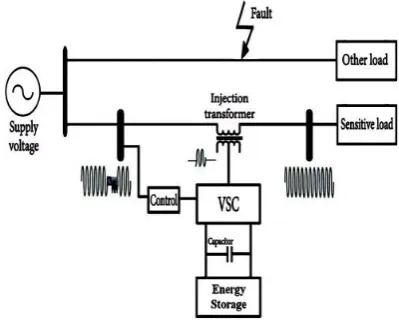
2.1.7 Dynamic Voltage Restorer:
In year of 1994, L. Gyugyi proposed a device and a method for dynamic voltage restoration of utility as per required in distribution network. This method uses active power in order to inject the faulted supply voltages and is locally known as the Dynamic Voltage Restorer. In this paper, a DVR design is essentially contains a voltage source inverter (VSI), an series injection transformer connected between the AC voltage supply and the non -linear load, a DC energy storage capacitor, and a control system as shown in Figure 2.
Fig -2: Basic DVR topology
[image:2.595.332.532.469.635.2]© 2018, IRJET | Impact Factor value: 6.171 | ISO 9001:2008 Certified Journal | Page 1192 supply real and imaginary power to the DVR. The controller
is more important part of the DVR for switching purposes. The switching converter is responsible to conversion process from DC to AC and to make sure that’s only the swell or sag voltage is injected to the series injection transformer. The phase transformers connection used in the three-phase DVR can be constructed either in delta/open or star/open connection. In case of asymmetrical fault on high voltage side, the zero sequence current flowing almost zero, if the distribution transformer connection in Ä-Y with the grounded neutral. In such a way of connection, the DVR is only used for the allegation of the positive and negative sequence.
3. COMPENSATION METHODS OF DVR
The type of the compensation technique mainly depends upon the specified factors such as DVR power ratings, various conditions of load, voltage sag type & swell. Some loads are non-linear towards phase angle l jump and some are sensitive towards change in magnitude and others are tolerant to these. Therefore, the control strategies mainly depend upon the type of load characteristics; there are three different methods of DVR series voltage injection which are:
(a) Pre-sag compensation (b) In-phase compensation
(c)Voltage tolerance method with minimum energy injection
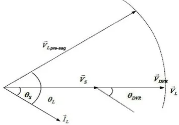
3.1.1 Pre-Sag/Dip Compensation Method:
The pre-sag method detects the supply voltage continuously and if it detects any disturbances in supply voltage by micro-controller it will inject the difference voltage between the sag and pre-fault condition, so that the load voltage can be restored by back to the pre-fault condition. Compensation of voltage sags in both phase angle and amplitude. Non-linear loads would be achieved by pre-sag compensation method. In this technique the series injected real power cannot be controlled and it is calculated by external conditions such as the type of faults and load conditions. The voltage of DVR is given below:
[image:3.595.336.514.277.401.2]VDVR = Vpre fault – Vsag
Fig -3: Phasor diagram of pre-sag/dip method
3.1.2 In-Phase Compensation Method:
[image:3.595.66.273.597.738.2]In this method the injected voltage is in phase with the supply side voltage regardless of the load current and pre-fault voltage. The phase angles of the pre-sag and load voltage are not similar but the vital criteria for power quality that is the constant magnitude of load voltage are fulfilled. The load voltage is given below:
|VL| = |Vpre-fault|
One of the advantages of this technique is that the amplitude of DVR injection voltage is minimum for some voltage sag in comparison with different strategies. Practical application of this technique is in non-sensitive loads to phase angle jump.
Fig -4: Phasor diagram of in-phase method 3.1.3 Voltage Tolerance Method with Minimum
Energy Injection:
A small jump in phase angle and a small drop in voltage can be tolerated by the load itself. If the phase angle variations between 5% -10% of nominal state and voltage magnitude lies between 90%-110% of nominal state that will not disturb the operational features of loads. Both phase and magnitude are the control parameter for this method and can be achieved by small energy injection. In this technique, the magnitude and phase angle of corrected load voltage inside the area of load voltage tolerance are changed. The phase angle jump and voltage drop on load can be accepted by load itself. The delicacy of loads to voltage magnitude and phase angle jump is different.
4. PROPOSED CONTROL TECHNIQUE
© 2018, IRJET | Impact Factor value: 6.171 | ISO 9001:2008 Certified Journal | Page 1193 PWM inverter, calculation of the compensating voltage and
stop triggering pulses when the occurrence has passed. The dq method gives the information of the phase shift (q) and depth (d) of voltage sag with start and end time. The load voltage is converted to VD, VQ and V0 based on park transformation according equations (1), (2) & (3).
4.1.1 Components and their rating:
Sr. No. Component Rating
1 PIC Microcontroller 32-Bit
2 Series Inverter 1kV
3 Thyristor 0.5kV
4 Capacitor Bank 300kVAR
5 Potential Transformer 230/5V 6 Zero Crossing Detector 5V
7 Opto-coupler 12V
8 Regulator IC 5V
9 Line Frequency 50Hz
10 Filter Inductance 7mH
11 Filter Capacitance 10μF
4.1.2 Design Criteria and Rated Power Calculations:
(1) Design criteria:
The design of the DVR is affected by the sensitive load, the supply characteristics and by the expected voltage-dip characteristics. When designing for a DVR for certain application, the following items should be considered:
Maximum load power and power factor:
The load size strongly affects the current rating of the voltage-source converter and the injection transformer as well as the need of energy storage needed.
Maximum depth and duration of voltage dips to be corrected:
These characteristics together with the load size, dictates the necessary storage capacity of the energy storage device. The maximum duration and penetration of voltage dips to be corrected is
determined by the statistics of the voltage dips at the DVR location and by the acceptable number of equipment trips.
Maximum allowed voltage drop of the DVR during the standby mode:
This effect is only for controlling mode during normal operation and indirectly the reaction speed at the beginning of a voltage dip.
Parameters of the step-down transformers:
Coupling of the step-down transformer (CIA or YIY, etc.) at input and output sides of the DVR.
Harmonic requirements of the load and of the system:
These affect the harmonic filtering needed for the DVR and also influence the choice of charging method for the capacitors. At the first instance when designing a DVR, some assumption could be made to simplify the analysis, such as:
Ideal switches
DC-side capacitors are large enough to maintain a ripple free DC bus voltage, even for unbalanced input voltage.
Series transformer and output filter components are ideal.
In order to design a DVR, the concept of “boost rating” is introduced to define the maximum voltage that the DVR is capable to inject into the power line with respect to the nominal distribution system voltage.
(2) Rated power calculations:
The DVR function, in case of voltage collapse, is for exchange real power between the power system and the energy storage device. The real power injected by the DVR is an important feature to precede its design process. To calculate the active and the reactive power, a factor is defined to indicate the reduction of the positive sequence voltage with respect to the nominal voltage of the load. For a certain supply voltage U, and required load voltage UL, the DVR injected voltage is written as:
Uc = UL –Us = (1-MF) UL
The range of the modulus of MF is defined by the maximum variation of Us, for which the DVR is designed. So, in normal operation MF should be unity and Uc is zero.
© 2018, IRJET | Impact Factor value: 6.171 | ISO 9001:2008 Certified Journal | Page 1194 Considering the fact that the DVR current should be
designed to be the same as the rated load current, the apparent power required by the DVR is then calculated in terms of the apparent load power, SL and MF by the following formula.
Sc = SL (1- MF)
Consequently, the active and reactive powers are calculated by separating Sc into its real and imaginary parts as
Where cos (ΦS) is the source power factor and cos(ΦL) is the load power factor.
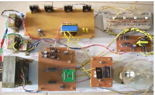
5. HARDWARE DESIGN
This is the hardware implementation of Dynamic Voltage Restorer (DVR) designed for mollification of voltage sags. The arrangement is of 10 sub-circuits as shown in the LA-SCR’s, DVR coupling network, Opto coupler circuit, Isolated power supply circuit, Lamp load, Line Impedance, PIC microcontroller circuit,1:1 isolated transformer, and the 3 transformers are:
1) For DVR DC Supply, 2) For trigger circuit, 3) For control circuit
In the below diagram, the 230V, 50 HZ supply is isolated by means of a 1:1 (230/230), 150VA isolation transformer. This isolated voltage is further steady state as the line voltage, which supplies power to the load, through simulated line impedance. The simulated line impedance is simply a wire wound resistor. To have maximum effect of voltage drop across the line impedance, the resistance value considered is of very high value, 120 Ohms. After this simulated line impedance, a switch is connected, through which the load can be connected or disconnected. In the recurring path, the DVR output is connected through the output winding of the coupling transformer developed. This output from the DVR is connected in series with the load, and mitigates the line impedance effect. The DVR circuit has to check the load voltage and need to be connected to the micro controller circuit and correct the voltage if there is any excess or absence when compared to a Reference voltage, by injecting appropriate voltage into the circuit by means of the coupling network.
[image:5.595.311.559.77.229.2]The authors can acknowledge any person/authorities in this section. This is not mandatory.
Fig -5: Hardware demonstration of Dynamic Voltage Restorer (DVR).
6. DYNAMIC VOLTAGE RESTORER
The functioning and designing of different blocks of dynamic voltage restorer is discussed herewith.
a) Single phase voltage source bridge inverter:
The voltage source inverter used in the DVR circuit makes the induction of required voltage with required phase possible. This inverter uses dc capacitors as the supply and can switch at a high frequency to generate a signal which will mitigate the voltage sags and swells across the load.
b) Micro controller circuit:
The microcontroller circuit is the heart of the system, and is responsible for generating the reference voltage waveform from the voltage waveform that is sampled from the sensing network, which it has obtained from the reference voltage sensing circuit. This reference voltage waveform is generated keeping the zero crossing as the reference to maintain the phase relationship of the load and correcting voltage. As the voltage induced through the coupling transformer, generated by the bridge inverter, the resulted voltage across the load will be a pure sinusoid of required voltage.
c) Opto coupler and driver circuits:
Opto couplers are having the capability of transferring an electrical signal between two circuits while electrically isolating the circuits from each other. They generally consist of an infrared LED, light emitting section at the input and a silicon photo detector at the output. The input for opto- couplers can be either AC or DC, which can drive the LED.
d) Coupling network:
© 2018, IRJET | Impact Factor value: 6.171 | ISO 9001:2008 Certified Journal | Page 1195 voltage source inverter to the load and at the same time need
to provide low impedance on the load side, so that the transformer winding itself doesn‟t provide a voltage drop across the load.
e) Inverter driving circuitry:
In order to trigger the LA-SCR, it is required to apply a +12V pulse to make it turn ‘ON’ and -12V pulse to turn it ‘OFF’ to the gate with respect to its emitter. Thus, in order to provide triggering pulses to each and every MOSFET, it is required to have four isolated power supplies of ± 12V which can be used to apply trigger pulses to the respective MOSFETs.
This inverter provides the required outputs, which can be used to drive the opto-coupler secondary side, which is meant for driving the LA-SCR gate.
f) Isolated power supplies for filter elements:
Three different power supplies are required, to provide power to various blocks of the over-all DVR circuit.
7. CONCLUSION
In this paper, hardware model of DVR is setup. The proposed method is used for identification of the voltage sag and is capable of mollification of the sag by keeping and maintaining the magnitude of load voltage at the voltage which is desired and THD within limits. The proposed method is very easy to understand and is reliable, has been used only for one switching per phase. Hence the system is easy, simple, but requires energy storage device as compared to commonly used DVR or STATCOM. The working performance of the proposed device is verified by theoretical results and is found to be satisfactory. This is the best control technique for non-linear loads which can’t withstand for phase angle jumps is pre-sag compensation. For minimum voltage injection, in-phase injection compensation is the best. For minimum energy insertion by the DVR, phase advance compensation is best but requires more voltage injection.
REFERENCES
[1] A.A.D.R. Perera, D.M. Vilathgamuwa, S.S. Choi,“Voltage
Sag Compensation with Energy Optimized Dynamic Voltage Restorer”, IEEE Trans. on Power Del., Vol. 11, No. 3, pp. 928-936, July 2003.
[2] V. Salehi, S. Kahrobaee, S. Afsharnia, “Power Flow
Control and Power Quality Improvement of Wind Turbine Using Universal Custom Power Conditioner”, IEEE Conference on Industrial Electronics, Vol. 4, pp. 1688-1892, July 2002.
[3] B.H. Li, S.S. Choi, D.M. Vilathgamuwa, “Design
Considerations on the Line-Side Filter Used in the Dynamic Voltage Restorer”, IEE Proc. Gener.
Transmission Distrib., Issue 1, Vol. 148, pp. 1-7, Jan. 2001.
[4] H.P. Tiwari, Sunil Kumar Gupta, “DC Energy Storage
Schemes for DVR Voltage Sag Mitigation System” International Journal of Computer Theory and Engineering, Vol. 2, No. 3, June, 2010.K. Elissa, “Title of paper if known,” unpublished.
[5] P. Boonchiam,N. Mithulananthan, “Understanding of
Dynamic Voltage Restorers through Matlab
Simulation” Thammasat Int. J. Sc. Tech., Vol. 11, No. 3, July-Sept. 2006.
[6] “Control and Testing of a Dynamic Voltage Restorer
(DVR) at medium Voltage Level,”IEEE Transactions on Power Electronics.Vol.19, no.3, MAY 2004.
[7] “Dynamic Voltage Restoration with Minimum Energy
Injection,” IEEE Transactions on Power Systems, Vol.15, No.1, February 2000.
[8] N.G.Hingorani, “Introducing custom power”, IEEE
Spectrum, pp.41-48, June 1995.
[9] M.F.McGrandghan, D.R.Mueller, and M.J.Samotyj.”Voltage
sags in industrial systems”, IEEE Trans. On industry applications, Vol.29, no.2,pp.397-402,March/ April 1993.
[10] S.W.Middlekauff and E.R.Collins Jr. “System and
customer impact consideration for series custom power devices,” IEEE Trans. On power Delivery, Vol. 13, no.1, pp. 278-282,Jan. 1998
[11] T.Wunderlin, P.Dahler, D.Amhof, and H.Gruning, “Power
supply quality improvement with a dynamic voltage restorer (DVR) “, in proceedings of EMPD‟98, Singapore, Mar.3-5, 1998 pp.518-525.
[12] A.Compos and G.Joos et.al. “ Analysis and design of a
series voltage unbalance compensator based on a three-phase VSI operating with unbalanced switching functions”, IEEE Trans. On Power Electronics, Vol.9, No.3, pp. 269-274, may 1994.
[13] R.Buxton, “Protection from voltage dips with the
dynamic voltage restorer”, in IEEE Half Day colloquium on Dynamic Voltage Restorer, London, 1998, Digest No. 1998/189.
[14] G.Nielsen, F.Blaabjerg, and N.Mohan,” control strategies
for dynamic voltage restorer compensating voltage saga with phase jump,” in proc, IEEE/APEC‟01 Conference, Vol. 2, 2001, pp.1267-1273.
[15] N.H.Woodly, L.Morgan, and A.Sundaram, “Experience
with an inverter-based dynamic voltage restorer,” IEEE Trans. Power delivery, Vol.14, pp.1181-1186, July 1999.
[16] “UNDERSTANDING POWER QUALITY PROBLEMS”,