© 2018, IRJET | Impact Factor value: 6.171 | ISO 9001:2008 Certified Journal | Page 2280
Analysis of Different Shape Slotted and Re-configurable Pin Diode
Based Microstrip Patch Antenna for x and ku Band Application.
Santosh Kumar Gupta
1, Anil Kumar
2, A.K. Jaiswal
31M.Tech Scholar, Dept. of Electronics & Communication Engineering, SIET, SHUATS, U.P, India 2Assistant Professor, Dept. of Electronics & Communication Engineering, SIET, SHUATS, U.P, India
3Head of the Dept. Electronics & Comm. Engineering, SIET, SHUATS, U.P, India
---***---Abstract -
This paper is about the design of three different proposed microstrip patch antenna incorporating slots and pin diode as switch (ON-OFF mode) for frequency re-configurability and advancement in antenna parameters. Microstrip line feeding technique is used. The antenna has been designed using Ansoft HFSS 13.0 and fabricated with substrate FR4_epoxy of thickness 1.8 mm. 1st antenna is about single band with edge and center slotted that has return loss -20.3466 dB at resonant frequency 11.1224 GHz, 2nd one is about dual band frequency excluding one slot and incorporating a pin diode at the patch center in between the slot and has return loss -29.0333 dB at resonant frequency 13.8776 GHz and the 3rd antenna is about dual band frequency incorporating two pin diode at both ends in the slot on patch at the center and has return loss -35.2532 dB at resonant frequency 13.7755 GHz. Moreover other parameters like VSWR, Gain, and Directivity have also been measured and values are best suited for designed antennas and are suitable for X and Ku band application.Key Words: Microstrip patch Antenna, Reconfigurable,
Slots, Pin Diodes, X and Ku, Dual Band, HFSS.
1. INTRODUCTION
Over the past few decades, Antenna Technology has been rapidly growing and involving innovative requirements in wireless communication system.[1][2][4] It has wide range of application like Wi-Fi, WLAN, Mobile Phone, GPS, Traffic Radar, Satellite, Biomedical, Military, Aerospace where antenna structure is the key part of the system.[3]
Microstrip patch antenna has drawn attention among others due to its noticeable advantages such as small size, low weight, small size, low manufacturing cost, ease of fabrication, ease of being integrated on the circuit.[6][7][10] Moreover it has dominant characteristics like low profile, multi band frequency, low radiation loss, integration with microwave integrated circuit and can be in any shape like rectangular, square, triangular, hexagonal, circular, elliptical and any others.[12][16]Furthermore microstrip patch antenna consists of a conducting ground plane at the bottom and metallic radiating patch at the top of comparatively thick dielectric substrate.[5][8]
In addition, Microstrip patch antenna structure can be described as sandwich of dielectric substrate in between two
parallel conducting layers. [13][15] Out of various feeding technique microstrip line feed has a conducting strip which is directly connected with the patch.[5][7] Likewise slots with the radiating patch have been fruitful for increasing the parameters, multiband frequency of microstrip patch antenna. In addition to acquire multiband frequency and to improve the performance of microstrip patch antenna re-configurability has drawn the attention of many researchers in recent time.[2][9] Re-configurability has been achieved by incorporating pin diode as switch (ON-OFF mode) which can be placed either in the slotted area or on the radiating patch.[3][8] Multiband, higher frequency such as X and Ku band as per IEEE Standard frequency range (8 to12)GHz X band and (12 to 18)GHz Ku band are back to back and separate with one another.[14][15] In this paper quad edge different slotted with pin diode at the centre in the radiating patch reconfigurable.
2. PROPOSED ANTENNAS
Three different antenna with different configuration is proposed in the paper. The configuration of three antennas is described here in brief:
Antenna 1:
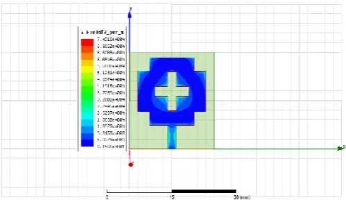
This antenna design is about quad edge and plus shape slotted center patch which gives single band of resonant frequency 11.1224 GHz. Figure 1(a) shows the design of proposed antenna 1.
Antenna 2:
This antenna design is about quad edge and rectangular shape slotted center patch with pin diode which gives resonant frequencies of 11.1224 GHz, 13.8776 GHz and13.9796 GHz. Figure 1(b) shows the design of proposed antenna 2.
Antenna 3:
© 2018, IRJET | Impact Factor value: 6.171 | ISO 9001:2008 Certified Journal | Page 2281 Figure 1(a) Antenna 1
Figure 1(b) Antenna 2
Figure 1(c) Antenna 3
2.1 CONFIGURATION FOR PROPOSED ANTENNAS
Three different microstrip patch antenna design has been proposed by incorporating slots and pin diodes in between slots. The antenna has been designed and tested by using Ansoft HFSS 13.0 software and the material selected for substrate is FR4_epoxy with thickness 1.8 mm having dielectric constant 4.4 and tangent loss 0.02. Microstrip line feeding technique has been used in these proposed antenna
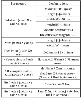
[image:2.595.303.566.134.457.2]to excite the patch. Below mentioned table describes about detail configuration of the proposed antennas.
Table -1: Configuration for Proposed Antenna 1, 2 and 3
Parameters Configurations
Substrate (x-axis X y-axis X z-y-axis)
Material=FR4_epoxy Length (L)=20mm Width(W)=20mm Height(H)=1.8mm Dielectric constant=4.4 Dielectric loss tangent=0.02
Patch (x-axis X y-axis) Length (L)=16mm width(W)=14mm Feed Point (x-axis X
z-axis) X=2mm and Z=-1.8mm
4 Square slots in Patch
(x-axis X z-axis) Slots each 2.75mm X 2.75mm at corner
2 Rectangular slots in patch (x-axis X z-axis)
slot 8mm X 2 mm at center slot 2mm X 8 mm at center , (Note: Not Used in Antenna 2) Pin Diode 1 (x-axis X
y-axis X z-y-axis) 1mm X 2mm X 1mm
Pin Diode 2 (x-axis X
y-axis X z-y-axis) 1mm X 2mm X 1mm, (Note: Not used in Antenna 2)
3. RESULTS AND DISCUSSION
.
The results obtained from simulation of three antennas with different configuration is discussed in this section.
3.1 Antenna 1
This antenna gives single band resonant frequency of 11.1224 GHz which shows the balanced value of the antenna parameters like return loss -20.3466 dB, vswr 1.6744, Gain of 4.8678 dB and Directivity 7.2616 also from the current distribution for E-Plane, it is observed that the antenna produces omnidirectional radiation throughout all resonant frequencies with stable radiation pattern and circular polarization. Table 3.1 describes the observed parameters of the proposed antenna structure and likewise figure 3.1 (a), (b), (c), (d), (e) and (f) represent the graphical pattern for return loss, vswr, gain, directivity, radiation Pattern and current distribution.
Table 3 -1: Observed values for antenna 1.
Frequenc
[image:2.595.299.566.136.458.2]© 2018, IRJET | Impact Factor value: 6.171 | ISO 9001:2008 Certified Journal | Page 2282 Figure -3.1 (a): Return Loss for Antenna 1.
Figure -3.1 (b): VSWR for Antenna 1.
Figure -3.1 (c): Gain for Antenna 1.
Figure -3.1 (d): Directivity for Antenna 1.
Figure -3.1 (e): Radiation Pattern for Antenna 1.
Figure -3.1 (f): Current Distribution for Antenna 1.
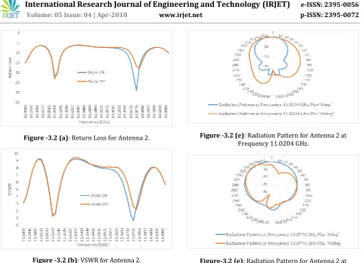
3.2 Antenna 2
Antenna 2 operation is based on the pin diode performance that is switching condition (ON-OFF). When the diode is at ON condition, the antenna gives the band of resonant frequency 11.0204 GHz and 13.9797. Similarly, during the OFF condition of diode the antenna gives resonant frequency of 11.0204 GHz and 13.8776 GHz. The observed values for return loss, vswr, gain, directivity for different frequencies at diode ON and OFF condition is summarized in table 3.2. From the current distribution for E-Plane, it is observed that the antenna produces omnidirectional radiation throughout all resonant frequencies with stable radiation pattern and circular polarization.The graphical pattern for return loss, vswr, gain, directivity, radiation pattern and current distribution is shown in the figure 3.2 (a),(b),(c),(d),(e) and (f) respectively.
Table -3.2: Observed values for antenna 2 for Pin Diode ON and Pin Diode Off.
Diode OFF
Frequency [GHz] Return loss VSWR Gain Directivity 11.0204 -23.1313 1.2133 3.501 6.4415 13.9797 -17.9164 2.2201 2.6863 5.5881
Diode ON
© 2018, IRJET | Impact Factor value: 6.171 | ISO 9001:2008 Certified Journal | Page 2283 Figure -3.2 (a): Return Loss for Antenna 2.
Figure -3.2 (b): VSWR for Antenna 2.
Figure -3.2 (c): Gain for Antenna 2.
Figure -3.2 (d): Directivity for Antenna 2.
Figure -3.2 (e): Radiation Pattern for Antenna 2 at Frequency 11.0204 GHz.
Figure-3.2 (e): Radiation Pattern for Antenna 2 at Frequency 13.8776 GHz.
Figure-3.2 (e): Radiation Pattern for Antenna 2 at Frequency 13.9797 GHz.
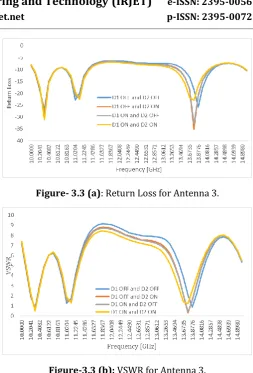
© 2018, IRJET | Impact Factor value: 6.171 | ISO 9001:2008 Certified Journal | Page 2284 3.3 Antenna 3
[image:5.595.306.560.40.414.2]This antenna 3 activities is based on the operation of two pin diode, i.e. pin diode 1 (D1) and pin diode 2 (D2) at switching condition (ON-OFF). At the initial condition when both the diode is OFF (D1 OFF and D2 OFF), the antenna gives the resonant frequencies of 11.0204 GHz and 13.8776 GHz. In addition, when the diode 1 (D1) is ON and diode 2 (D2) is OFF the antenna gives resonant frequencies of 11.0204 GHz and 13.7755 GHz with slight increase in the values of antenna parameters. Similarly when diode 1 (D1) is ON and diode 2 (D2) is OFF the antenna gives the same resonant frequencies of 11.0204 GHz and 13.7755 GHz with considerable improvement in the antenna parameter values. Finally when both the diode 1 (D1) and diode 2 (D2) are ON, the antenna gives the resonant frequencies of 11.0204 GHz and 13.6735 GHz with remarkable improvement in the values of the antenna parameters. The observed values of antenna parameters like return loss, vswr, gain and directivity for different condition of diode1 (D1) and diode 2 (D2) are summarized in the table 3.3. Current distribution for the E-Plane observed that antenna produces omnidirectional radiation throughout all resonant frequencies with stable radiation pattern and circular polarization.
Table-3.3: Observed values for antenna 3 for both Pin Diode1 (D1) and Pin Diode2 (D2) at (ON-OFF) condition.
D1 OFF and D2 OFF Frequency
[GHz] Return loss VSWR Gain Directivity 11.0204 -22.8154 1.2584 3.611 6.3837 13.8776 -25.8827 0.8832 3.973 6.483
D1 OFF and D2 ON Frequency
[GHz] Return loss VSWR Gain Directivity 11.0204 -21.0595 1.5417 3.6394 6.3964 13.7755 -35.2532 0.3001 4.45 6.8784
D1 ON and D2 OFF Frequency
[GHz] Return loss VSWR Gain Directivity 11.0204 -20.6512 1.6163 3.6441 6.3802 13.7755 -33.1656 0.3816 4.445 6.8867
D1 ON and D2 ON Frequency
[GHz] Return loss VSWR Gain Directivity 11.0204 -19.3833 1.8722 3.6822 6.4205 13.6735 -21.8228 1.4114 4.8811 7.2693
The graphical pattern for return loss, vswr, gain, directivity, radiation pattern and current distribution are shown in the figure 3.3 (a),(b),(c),(d),(e) and (f) respectively.
Figure- 3.3 (a): Return Loss for Antenna 3.
Figure-3.3 (b): VSWR for Antenna 3.
Figure-3.3 (c): Gain for Antenna 3.
[image:5.595.58.561.384.747.2] [image:5.595.33.305.419.705.2]© 2018, IRJET | Impact Factor value: 6.171 | ISO 9001:2008 Certified Journal | Page 2285 Figure-3.3 (e): Radiation pattern for Antenna 3 at
frequency 11.0204 GHz.
Figure-3.3 (e): Radiation pattern for Antenna 3 at frequency 13.8776 GHz.
Figure-3.3 (e): Radiation pattern for Antenna 3 at frequency 13.7755 GHz.
Figure-3.3 (e): Radiation pattern for Antenna 3 at frequency 13.6735 GHz.
Figure-3.3 (f): Current Distribution for Antenna 3.
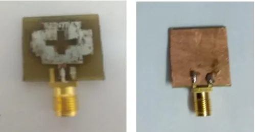
4. FABRICATION
[image:6.595.48.566.52.222.2]This portion explains the fabrication of microstrip patch antenna 1, which was designed and simulated in above section. The dimensions used for the fabrication is obtained from simulation. Material used for fabrication is substrate FR4_epoxy and SMA connector. Figure 4.1 and 4.2 shows the top and bottom view of the antenna.
[image:6.595.310.560.359.489.2]Figure-4.1: Antenna 1 prototype (top and bottom view) and Antenna 3 without Diode D1 & D2.
Figure-4.2: Antenna 2 prototype (top and bottom view) without Diode D1.
5. CONCLUSION
[image:6.595.311.558.532.656.2]© 2018, IRJET | Impact Factor value: 6.171 | ISO 9001:2008 Certified Journal | Page 2286 results for the slotted and frequency reconfigurable
antennas have been discussed in this paper. In addition, it has been observed that with slots of different shapes and size, the radiating area of the patch decreased slightly but the performance of antennas increased. Slots and pin diodes were introduced for both frequency and antenna parameters re-configurability, the diodes have been incorporated over the patch at the center in between slotted area.
The above results have made clear that the slotted antenna 1 works for single band resonant frequency 11.1224 GHz and has attractive values of return loss, vswr, gain, directivity and radiation pattern. It has been analyzed that by introducing slots and pin diodes for frequency re-configurability, the values in return loss, vswr, gain and directivity significantly increase without affecting the results. Furthermore, by using the single pin diode in antenna 2 with only one slot at the center of the patch the antenna works for dual band resonant frequencies of 11.0204 GHz, 13.8776 GHz and 13.9797 GHz during diode OFF-ON condition and also by incorporating two pin diodes, the antenna works for different resonant frequencies of 11.0204 GHz, 13.6735 GHz, 13.7755 GHz and 13.8776 GHz during different diode OFF-ON condition. It has also been observed that the designed antennas produce omnidirectional radiation throughout all operating band of resonant frequencies with stable radiation pattern and circular polarization. These proposed antennas have potential to be used in different areas of application like satellite communication, broadband communication, radar, space, aeronautical radio navigation, mobile satellite.
REFERENCES
[1] Symeon Nikolaou, Boyon Kim and Photos Vryonides, “Reconfiguring Antenna Characteristics Using PIN Diodes”,3rd European Conference on Antenna & Propagation, pp3748-3752,2009.
[2] M. T. Ali, N. Ramli, M.K.M.Salleh and M.N.Md.Tan, “A Design of Reconfigurable Rectangular Microstrip Slot Patch Antennas”, IEEE International Conference on System Engineering and Technology (ICSET),pp. 111-115 ,2011.
[3] R.Er-rebyiy, J.Zbitou, A.Tajmouati, M.Latrach, A.Errkik and R.Mandry, , “A New Design of U Shaped Reconfigurable Antenna Based on PIN diodes”, International Conference On Wireless Technology, Embedded and Intelligent System, pp. 1-4,2017.
[4] N. Ramli, M. T. Ali, A. L. Yusof, S. Muhamud - Kayat, and A. A. A. Aziz, “PIN Diode Switches for Frequency-Reconfigurable Stacked Patch Microstrip Array Antenna using Aperture-Coupled Technique”, Asia-Pacific Microwave Conference Proceedings, pp.1052-1054,2013.
[5] T. Sabapathy, M.A. Bashah, M. Jusoh, P.J. Soh and M.R. Kamarudin, “Frequency Reconfigurable Rectangular Antenna with T Slotted Feed Line”, International Conference on Radar, Antenna, Microwave, Electronics, and Telecommunications, pp.81-84,2016.
[6] Ahmed E. Zahran and Mahmoud A. Abdalla, “Compact Single/Multi Bands Frequency Reconfigurable Antenna Using PIN Diode Controlled Meta-surface”, IEEE International Symposium on Antennas and Propagation & USNC/URSI National Radio Science Meeting,9-14 July 2017.
[7] Aishwarya Sudarsan and Apeksha Prabhu, “Design and Development of Microstrip Patch Antenna”, International Journal of Antennas (JANT) Vol.3, No.1/2/3, July 2017.
[8] Amruta Murkute and Harbinder Singh, “ Line Feed Microstrip Patch Antenna for Lowest Frequency Microwave Band”, International Journal of Computer Applications (0975 – 8887) and National Conference on Latest Initiatives& Innovations in Communication and Electronics (IICE 2016),2016.
[9] Rajendra Soloni, Rajappa H S and Dr.Chandrappa D N, “Design and Analysis of MultibandReconfigurable Microstrip Patch Antenna with Switchable Element”, 2017 International Conference on Advances in Computing, Communication and Informatics (ICACCI), pp.288-293,13-16 Sept. 2017.
[10] Sumit Jain and Manoj Rawat, “Multiband T-Slot Microstrip Patch Antenna”, International Academy of Engineering and Medical Research, Volume-2, ISSUE-2, February 2017.
[11] Samiya Murtaza and Anas Iqbal, “Design of a Compact UWB F-Slotted Microstrip Antenna for Wireless Applications”, International Journal of Advanced Research in Computer Engineering & Technology (IJARCET) Volume 6, Issue 4, ISSN: 2278 – 1323, April 2017.
[12] Neha Gupta, “Effects of Slots on Microstrip Patch Antenna”, International Research Journal of Engineering and Technology (IRJET), Volume 04, Issue 02, Feb -2017.
[13] A. R. Chaudhari, “Effect of Wide Slots on Bandwidth & Gain of Broadband Microstrip Antenna”, International Journal of Engineering Technology Science and Research (IJETSR), ISSN 2394 – 3386, Volume 4, Issue 4, April 2017
© 2018, IRJET | Impact Factor value: 6.171 | ISO 9001:2008 Certified Journal | Page 2287 [15] Madhukant Patel, Piyush Kuchhal, Kanhiya Lal and
Ranjan Mishra, “Design and Analysis of Microstrip Patch Antenna Array Using Different Substrates for X-Band Applications”, International Journal of Applied Engineering Research ISSN 0973-4562 Volume 12, Number 19 (2017) pp. 8577-8581.
[16] Sarthak Singhal, “Microstrip Antenna for X and Ku Band”, International Journal of Electronics and Computer Science Engineering, ISSN-2277-1956 Volume 1, Number 3, pp. 834-839.M
BIOGRAPHIES
Mr. Santosh Kr. Gupta is an M. Tech Scholar at Dept. of Electronics and Communication Engineering, SIET, SHUATS, Allahabad. He has completed his Bachelor of Engineering from Kantipur Engineering College (T.U), Kathmandu, Nepal in Electronics and Communication Engineering. He is also an active student member of IEEE. His area of interest is Telecommunication, Microwave Communication and Antenna Design.
Dr. Anil Kumar is Assistant Professor at the Dept. of Electronics and Communication Engineering, SIET, SHUATS, Allahabad. He has extensive teaching experience of 14 years. His areas of interest is Reconfigurable Antenna Design, Artificial Neural Networks and VLSI.