Abstract—We have performed an exploration of inverted rib waveguide platform for use in optical backplanes. This entailed the design, optimization, and characterization of a variety of passive optical components that may serve as a basis for the functions required of an on-chip optical networks. The presented design introduces an inverted-rib template which consists of a polymer waveguide layer. We have successfully fabricated and demonstrated low-loss waveguides, and also functional passive devices such as directional couplers, multi-mode interferometers, waveguide bends and crossings, and distributed Bragg reflectors. We also demonstrate a way of coupling active components (e.g. in silicon) to such a photonic integrated circuit.
Index Terms—Optical backplane, opto-electronic integration, polymer waveguide, passive optical components.
I. INTRODUCTION
ECENT advances in CMOS technology mean that the data rate bottleneck for computing is shifting from data processing to short range data transmission. This limitation stems from the fact that traditional copper wires experience exponentially increasing losses as the bit rate of the transmitted signal increases, imposing speed and distance limitations for reliable data transfer. Optical interconnects are becoming the preferred alternative to electrical connections as they do not suffer from the frequency-dependent losses [1]. An additional benefit of optical interconnections is the possibility to provide Wavelength Division Multiplexing (WDM). Already, optical technology is viable for long distance connections such as long haul telecommunications, and even the shorter range connections (>1m) in high power computer systems [2]. These short reach optical connections use single channel links based on Vertical Cavity Surface Emitting Lasers (VCSEL) and have been effective in alleviating the data bottleneck so far, but they exhibit limited scalability in terms of cost, efficiency and footprint as the data transmission bottleneck progresses downwards to chip-scale communications/links. A bundle of fibers is also bulky and
This paragraph of the first footnote will contain the date on which you submitted your paper for review.
This work is supported by an EPSRC Doctoral Prize and a European Research Council Starting grant (no. 337508).
K. Debnath, R. Moore, A. Liles and L. O’Faolain are with School of Physics & Astronomy, University of St Andrews, North Haugh, St Andrews KY16 9SS, UK (email: [email protected]).
Color versions of one or more of the figures in this letter are available online at http://ieeexplore.ieee.org
difficult to handle, much like electrical wiring before the invention of the printed circuit board (PCB). The solution to this problem is envisioned in the development the optical equivalent; the optical printed circuit board or O-PCB [3]. This would consist of a board pre-printed with an arrangement of waveguides that would serve as the communication channels between chips. The chips themselves would still receive power and control signals through electrical connections embedded in the board, but all the high-speed data transmission would be routed through the optical links.
In this work, we demonstrate a polymer-based inverted rib waveguide platform which could fulfill the efficiency, scalability and cost requirements needed to displace chip-scale electrical interconnects. A fully operational optical routing system, i.e. O-PCB would consist not only of simple straight line waveguides, but also passive optical devices for splitting, routing, and filtering purposes. Many devices that perform these functions have been demonstrated previously with silicon waveguide structures [4]. However, due to its large index contrast, silicon based components are more prone to optical losses arising from any fabrication imperfections than polymer based components. Here, using the inverted rib configuration of [5], we realize a variety of polymer based passive optical components such as waveguide crossings and bends, multimode interferometers (MMI), directional couplers and distributed Bragg reflectors, which are important for the creation of advanced Photonic Integrated Circuits (PIC). Finally we demonstrate a method of coupling light from these waveguides to active components such as electro-optic modulators and detectors.
II. INVERTED RIB STRUCTURE
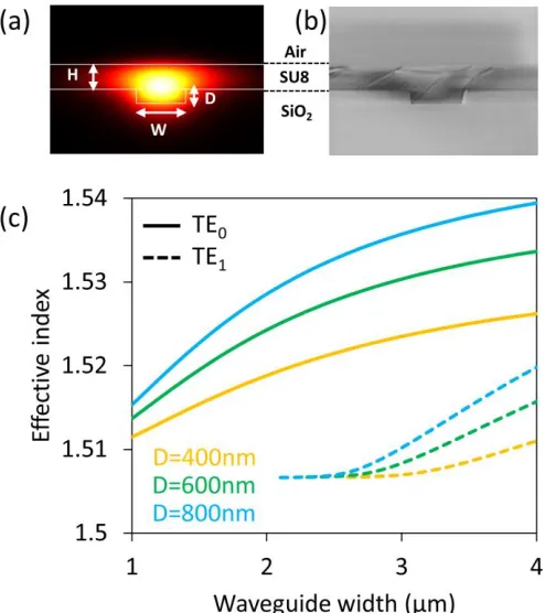
Multi-mode polymer waveguides for chip-to-chip communications have previously been demonstrated [3] with very low propagation loss. These are sufficient for point-to-point transmission, but in order to implement additional functionality, single mode operation is a prerequisite. The basic structure for our designs is shown in Fig. 1. The substrate is silica in which a trench is etched. A layer of SU8 polymer is deposited on top creating the inverted rib waveguide structure [5]. The design of our waveguide was carried out using COMSOL and optimized for single mode operation in the C-band. The refractive indices of SU8 and silica used for the simulation are 1.58 and 1.44 respectively. Figure 1a shows the TE mode profile and Fig. 1b shows the SEM image of the cross section of the inverted rib waveguide.
Toolkit for Photonic Integrated Circuits Based
on Inverted Rib Waveguides
Kapil Debnath, Rowan Moore, Alexandros Liles and Liam O’Faolain
Figure 1c shows the effective indices of the fundamental and the second order TE modes for different etch depths and waveguide widths. In order to maintain single mode operation, all the devices discussed here consist of waveguides with a trench depth (D) of 600nm, trench width (W) of 2μm and a slab thickness (H) of 1μm. These values were chosen to reduce the fabrication complexity and can easily and reliably be achieved using photolithography or nano-imprinting techniques for mass production [5]. In this work, we use electron beam lithography due to its flexibility and suitability for rapid prototyping.
Fig. 1. (a) Electric field distribution of the fundamental TE-polarized mode in an inverted rib waveguide with W=2µm, D=0.6µm and H=1µm. (b) SEM image of the cross section of the inverted rib waveguide. (c) Change in effective index of the fundamental (solid line) and first order (dashed line) TE modes as the width of the waveguide and etch depth is varied. The operating wavelength considered here is 1.55µm.
Fabrication of the devices was carried on a 5μm thick thermally oxidized silicon substrate. Using electron beam lithography, the waveguide patterns were defined in a ZEP-520A resist layer and the pattern is transferred into the SiO2 layer using reactive ion etching. The chip was then spin-coated with a layer of SU8. After curing at 200oC for 1 hour the final thickness of SU8 was 1μm. Finally, the chip was cleaved to obtain optical facets for characterization and testing.
The fabricated devices were characterized using an end-fire setup. Here we used an amplified spontaneous emission (ASE) source with the center wavelength at 1570nm and bandwidth of 100nm. Here we have only selected the TE polarized component of the ASE output by using a polarizing beam splitter. The TE polarized light is then coupled into the waveguides via an objective lens. The output of the
waveguides is collected using another objective lens and sent to the photo detector. Figure 2a shows a typical transmission spectrum of a 2mm long inverted rib waveguide. In order to measure the transmission loss of straight waveguides we used the cutback method. The inset in the Fig. 2a shows the normalized transmission loss for different waveguide length and the transmission loss was found to be 1dB/cm, comparable to that reported in [6]. The use of polymers such as the ORMOCER series can further reduce the transmission loss, due to their intrinsic low material loss, as highlighted in [7].
Fig. 2. (a) Transmission spectrum of an inverted rib waveguide. The spectrum is normalized by the source spectrum. The fibre-to-fibre loss is approximately 12dB. The inset shows the transmission loss as a function of waveguide length, which is normalized by the output spectrum of the measurement setup without the device, thus only includes the coupling losses to the devices. (b) Insertion loss per 90o bend for different bending radii. Inset shows the
schematic representation of the design used to test bending radius. For bending radius above 1mm, the loss per mm does down to sub-dB.
[image:2.612.50.297.185.463.2] [image:2.612.317.560.188.574.2]width of 2μm, while varying the radius of the bends along the waveguide. The waveguides included four 90o bends. The bending radii of each of the waveguides ranged from 0.5mm to 2.0mm. The measured loss per 90o bend for different bending radii is shown in Fig. 2b. For bending radii larger than 1 millimeter, the bending loss is less than 1dB per 90o bend.
III. OPTICAL COMPONENTS
We have successfully demonstrated several different functional passive devices using this waveguide configuration, as described below.
A. Multimode Interference Coupler
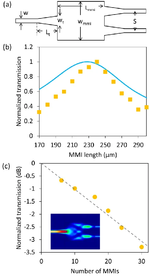
Optical devices utilizing MMI couplers are incorporated in many integrated components, such as electro-optic modulators [8], ring lasers [9], multiplexers [10] etc. The MMI coupler is based on a multimode waveguide which can support a large number of modes. Using the self-imaging property of the multimode section, compact power splitters and combiners can be realized. Here we use inverted rib structure to implement a 1x2 MMI power splitter. The length of the MMI section needs careful design to optimize the imaging of the light from the input to the two output ports. According to [11], the MMI length varies quadratically with the width of the MMI and based on 2D approximation, the length of the MMI is given by Lmmi=3π/8(β0 –β1). Here β0 and β1 are the propagation constants of the fundamental and first order excited modes in the MMI region. For estimating the design parameters, we used the fully vectorial simulation tool FIMMWAVE. The width of the multimode waveguide section is chosen to be wmmi=20µm, which supports around nine TE modes. The values for the propagation constants for the fundamental and first excited modes as calculated using FIMMWAVE were 6.2039x10⁶ m-1 and 6.1987x10⁶ m-1 respectively. The position of the twofold image is therefore at a length of 226.5μm. Results of the simulation also indicated that the maximum transmission occurs at a length of 230μm, closely matching this value. The center-to-center spacing of the output waveguides for optimum coupling was subsequently found to be S=10.8μm. This minimizes any coupling between the output waveguides while keeping the overall size of the device small. We also introduced linear tapers [12] at the input and output ports to further reduce any coupling losses between the access waveguides and the MMI region.
The input and output waveguide width was w=2µm and the tapered section was Lt=200um long and expanded to wt=6µm near the MMI region. The MMI width was kept fixed at 20µm and the length was varied from 170μm to 310μm. In Fig. 3a the blue curve and the yellow squares represent the simulated and measured output power respectively for different MMI lengths, which are normalized with respect to the highest output power. The peak in transmission occurs for a length of 240μm rather than the expected 230μm. This is most likely due to a slight mismatch between the parameters used in the simulation and the dimensions of the fabricated device. In order to measure the insertion loss for the MMI devices, we
fabricated a set of devices with multiple MMIs chained together. In Fig. 3b we estimate the transmission per MMI using a fit on the measurements at a wavelength of 1550 nm. The loss per MMI is 0.115 dB, which shows a significant improvement over the previously reported value of 1.3dB for Su8 ridge waveguides [Yang]. We have also observed a relatively broadband response of the MMI with the transmission varying by less than a 1dB over the 100nm wavelength range of the ASE source.
Fig. 3. (a) Schematic diagram of the MMI design. The values of different dimensions are given in the text. (b) Simulation and measured transmitted power (normalized against the highest output power) for different MMI length (Lmmi). (c) Insertion loss as a function of number of MMIs. Here a 240µm long
MMI was considered. Inset shows electric field distribution in a 1x2 MMI.
B. Directional Coupler
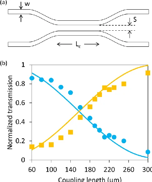
[image:3.612.314.563.162.618.2]length over which light from one waveguide completely transfers to the second one is known as the coupling length and is given by Lc=π/(βs-βa). βs and βa are the propagation constants of symmetric and antisymmetric modes present in the coupling region. We used FIMMWAVE to estimate the coupling length of a direction coupler realized using the inverted rib platform. The width of the waveguides was w=2.1μm and the separation between them was S=1.9μm. Bent waveguides with 1mm bending radius were used both in the input and output sides of the directional coupler to avoid any unwanted coupling. The coupling length was calculated to be Lc= 329μm, in good agreement with Lc= 320μm, the value obtained from simulations. A set of directional couplers was fabricated, with target design parameters equal to those used in the simulation. The devices spanned a range of coupling lengths from 50μm to 400μm. Figure 4 shows the measured values of fractional transmission in the direct waveguide and the coupled waveguide, along with simulated power splitting, at 1550nm wavelength. The measured coupling length for 3dB splitting is 170µm, showing a good agreement with the simulated value.
Fig. 4. (a) Schematic diagram of the directional coupler. The values of different dimensions are given in the text. (b) Dependence of the transmitted power, at a wavelength of 1550nm, through the direct arm and the coupled arm on the coupling length. Yellow squares (yellow line) and blue circles (blue line) are the measured (simulated) power for the coupled arm and the direct arm respectively.
C. Waveguide Crossing
Waveguide crossings are also very important components for planar optical circuits. It is very difficult to achieve any complex 2D photonic circuits without the use of low-loss and crosstalk waveguide crossings. In order to achieve
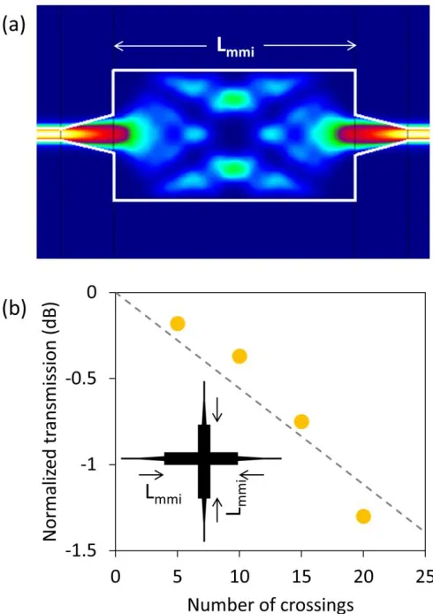
low-loss and low-crosstalk waveguide crossings there are different designs proposed in the literature [13-16]. Among them MMI based crossings are the most popular. Here we use 1x1 MMI structure to realize low-loss waveguide crossing. In the multimode region of an MMI device, the 1/e width of the optical field increases and decreases periodically, as shown in Fig. 5a. For a 1x1 MMI device, at the half of the device length the optical field decreases to two self-images of the input optical field. At that position there is very little optical field around the sides of the waveguide. Therefore any perturbation at these positions will have a minimal effect on the propagation of the optical field. The inset in Fig. 5b shows the waveguide crossing design using 2 perpendicularly placed 1x1 MMI structures.
[image:4.612.51.294.311.602.2]Fig. 5. (a) Electric field distribution in a 1x1 MMI. The physical boundary of the MMI is highlighted by white boundary. At the half of the MMI length there is very little field around the sides of the MMI section and hence placing another MMI vertically will cause very little perturbation to the field. (b) Insertion loss as a function of number of MMI crossings. The inset shows the waveguide crossing design using 2 1x1 MMI.
D. Distributed Bragg Reflector
Distributed Bragg Reflectors (DBR) can be realized using the inverted rib structure. In order to design the DBR, we change the width of a waveguide thus changing the effective refractive index experienced by the guided mode. A diagram of the device is shown in the inset of Fig. 6. For this design we choose to alternate the width of the waveguide between 2um (i.e. the standard width of the waveguide) and 3um. FIMMWAVE was used to calculate the effective index of the fundamental TE mode for each of these dimensions giving values of 1.5252 and 1.5296 for the 2μm and 3μm waveguides respectively, at 1550nm wavelength. Aiming for a stop band in the C-band, the DBR section was designed with a period of 500nm and waveguide sections of 250nm each. The total number of periods included in the device was 4000, producing final device length of 2mm. Figure 6 shows the normalized transmission spectrum of the device. As expected, there is a strong extinction of the transmitted light in a narrow window, flanked by further drops in transmission of steadily decreasing magnitude. The extinction ratio around the stop band region is 25dB, comparable to the values reported previously for polymer waveguide based DBRs [Yun]. The width of the main
stop band also matches well with the simulation, with a full width at half maximum of 2.8nm for the simulation and 2.5nm for the experiment. This slight mismatch is probably due to a small variation in the fill factor along the grating. The simulated transmission spectrum was also shifted by 9nm to match the stop band centers. This is most likely caused by a variation between the simulated and the actual effective refractive index.
Fig. 6. Yellow dashed curve and blue curve represent the simulated and measured transmission spectra of the DBR respectively. The DBR structure is shown in the inset.
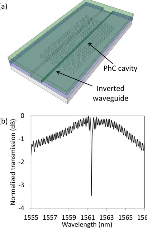
IV. COUPLING TO A SILICON PHOTONIC CRYSTAL In the previous section we discussed different passive optical components realized using inverted rib structure for their use in O-PCBs. To increase the functionality of the PIC, it is desirable to incorporate active components. Here we demonstrate a method of connecting a network of passive optical components with optical components in silicon. In this demonstration we use the technique introduced in [17] to couple light from a dielectric waveguide to a photonic crystal cavity in silicon. This system acts as a notch filter which can, when combined with an integrated pn junction, be used to modulate [18] or detect optical signal [19]. As shown in Fig. 7a an inverted rib waveguide is placed in the close proximity of a photonic crystal (PhC) cavity. Light propagating through the waveguide couples into the cavity at cavity resonance, which results in a dip in transmission.
[image:5.612.49.294.50.397.2] [image:5.612.315.560.151.368.2]as the substrate for the inverted rib waveguide and c) acts as a buffer layer between the inverted rib waveguide and the PhC cavity. A 2µm wide and 600nm deep trench was defined in the FOx layer above the PhC cavity by means of e-beam lithography and RIE. Finally a 1um thick layer of SU8 was applied to the sample using spin-coating to form the inverted rib waveguide.
Figure 7b shows the experimental transmission spectrum of an inverted rib waveguide, vertically coupled to a PhC cavity. The dip in the transmission near 1561nm corresponds to the resonance wavelength of the PhC cavity. From the spectrum, the measured Q-factor is 20,000 with an extinction ratio of 3.5dB, this corresponds to intrinsic Q-factor of 29,000 (according to [21]). The extinction ratio can further be improved by improving the K-space matching between the waveguide mode (by changing the waveguide design and/or waveguide material) and the PhC mode (by optimally designing the PhC cavity) as discussed in [17]. The ripples visible in the spectrum are caused by the reflections from the waveguide facets, which can be eliminated by using anti-reflection coatings. Here, for demonstration purposes, we followed a monolithic fabrication process. A more versatile process such as adhesive bonding [22] can also be adopted for bonding silicon components to an inverted rib waveguide platform.
Fig. 7. (a) Schematic diagram of the system where an inverted rib waveguide is vertically placed on top of a photonic crystal cavity, (b) Transmission spectra of the inverted rib waveguide, the dip correspond to the cavity resonance.
V. CONCLUSION
Optical-PCBs based on low loss polymer waveguides and passive optical components offer additional options for integrated optical circuits. In this work, using a polymer-based inverted rib waveguide design, we have successfully demonstrated a range of passive devices for optical signal routing. The performance of waveguide bends were studied and sub-dB bending loss was obtained for bending radius above 1mm. Very low loss MMI devices, 0.1dB, have been demonstrated, which opens up the possibility of designing different routing and coupling components, as well as wavelength multiplexing and demultiplexing elements based on inverted rib structure. Directional couplers based on inverted rib waveguides have also been investigated and a coupling length of 170um have been found for a waveguide separation of 2µm, which implies that very short optical components such as splitters and couplers can be realized. Using 1x1 MMI, waveguide crossings with sub-dB insertion loss were demonstrated, which are essential for designing complex planar integrated circuits. We have also realized DBR with 2.5nm stop band by periodically varying the width of the inverted rib waveguide. Finally by placing inverted rib waveguide on top of a silicon based photonic crystal cavity, we demonstrate the possibility of coupling such passive structures to active electro-optic components. To our knowledge, this study is the first time that passive optical components devices have been fabricated using a polymer inverted-rib configuration. The success of this investigation combined with a high efficiency and low-cost route to large-area processing, such as nanoimprint lithography or photolithography, represents a promising route towards the realisation of a fully functional and WDM-capable optical backplane.
REFERENCES
[1] D. A. B. Miller, “Device Requirements for Optical Interconnects to Silicon Chips,” Proceedings of the IEEE, vol. 97, no. 6, pp. 1166-1185, Jul. 2009.
[2] M. A. Taubenblatt, “Optical Interconnects for High-Performance Computing,” J. Lightw. Technol., vol. 30, no. 4, pp. 448-457, Oct. 2012. [3] F. E. Doany, C. L. Schow, B. G. Lee, R. A. Budd, C. W. Baks, C. K. Tsang, J. U. Knickerbocker, R. Dangel, B. Chan, H. Lin, C. Carver, J. Huang, J. Berry, D. Bajkowski, F. Libsch, and J. A. Kash, “Terabit/s-class optical PCB links incorporating 360-Gb/s bidirectional 850 nm parallel optical transceivers,” J. Lightw. Technol., vol. 30, no. 4, pp. 560-571, Nov. 2011.
[4] G. T. Reed, Silicon Photonics: The State of the Art, Chichester, U.K.: Wiley, 2008.
[5] M. Wang, J. Hiltunen, S. Uusitalo, J. Puustinen, J. Lappalainen, P. Karioja, and R. Myllylä, “Fabrication of optical inverted-rib waveguides using UV-imprinting,” Microelec. Eng., vol. 88, no. 2, pp. 175-178, Oct. 2012.
[6] B. Yang, L. Yang, R. Hu, Z. Sheng, D. Dai, Q. Liu, and S. He, “Fabrication and characterization of small optical ridge waveguides based on SU-8 polymer,” J.Lightw. Technol., vol. 27, no. 18, pp. 4091-4096, May 2009.
[image:6.612.51.287.357.725.2]Wachter, and A. Brauer, “Inorganic organic hybrid materials for application in optical devices,” Thin Solid Films, vol. 442, no. 1, pp. 194-200, Sept. 2003.
[8] L. Liao, A. Liu, D. Rubin, J. A. B. J. Basak, Y. A. C. Y. Chetrit, H. A. N. H. Nguyen, R. A. C. R. Cohen, N. A. I. N. Izhaky, and M. A. P. M. Paniccia, “40 Gbit/s silicon optical modulator for high-speed applications,” Elect. Lett., vol. 43, no. 22, pp. 1196-1197, Oct. 2007. [9] R. V. Roijen, E. C. M. Pennings, M. J. N. Van Stalen, T. V. Dongen, B.
H. Verbeek, and J. M. M. Van der Heijden, “Compact InP‐based ring lasers employing multimode interference couplers and combiners,” Appl. Phys. Let., vol. 64, no. 14, pp. 1753-1755, Apr. 1994.
[10] M. R. Paiam, and R. I. MacDonald, “Design of phased-array wavelength division multiplexers using multimode interference couplers,” Appl. Opt., vol. 36, no. 21, pp. 5097-5108, Jul. 1997.
[11] L. B. Soldano, and E. C. M. Pennings, “Optical multi-mode interference devices based on self-imaging: principles and applications,” J. Lightw. Technol., vol. 13, no. 4, pp. 615-627, Apr. 1995.
[12] D. J. Thomson, Y. Hu, G. T. Reed, and J.-M. Fedeli, “Low loss MMI couplers for high performance MZI modulators,” IEEE Photon. Technol. Lett., vol. 22, no. 20, pp. 1485-1487, Oct. 2010.
[13] Yang, L., Yang, B., Sheng, Z., Wang, J., Dai, D., & He, S. (2008). Compact 2x2 tapered multimode interference couplers based on SU-8 polymer rectangular waveguides. Applied Physics Letters, 93(20), 203304.
[14] W. Bogaerts, P. Dumon, D. V. Thourhout, and R. Baets, “Low-loss, low-cross-talk crossings for silicon-on-insulator nanophotonic waveguides,” Opt. let., vol. 32, no. 19, pp. 2801-2803, Oct. 2007. [15] H. Liu, H. Tam, P. K. A. Wai, and E. Pun, “Low-loss waveguide
crossing using a multimode interference structure,” Opt. comm., vol. 241, no. 1, pp. 99-104, Jul. 2004.
[16] H. Chen, and A. W. Poon, “Low-loss multimode-interference-based crossings for silicon wire waveguides,” IEEE Photon. Technol. Lett.,
vol. 18, no. 21, pp. 2260-2262, Nov. 2006.
[17] Hashim, A., Bamiedakis, N., Penty, R. V., & White, I. H. (2013). Multimode polymer waveguide components for complex on-board optical topologies.Lightwave Technology, Journal of, 31(24), 3962-3969.
[18] Yun, B., Hu, G., Zhang, R., & Cui, Y. (2015). Fabrication of a third-order polymer chirped waveguide Bragg grating with tapered core size by contact lithography. Applied Optics, 54(3), 467-471.
[19] C.-H. Chen, and C.-H. Chiu, “Taper-integrated multimode-interference based waveguide crossing design,” IEEE J. Quant. Elect., vol. 46, no. 11 pp. 1656-1661, Nov. 2010.
[20] K. Debnath, K. Welna, M. Ferrera, K. Deasy, D. G. Lidzey, and L. O’Faolain, “Highly efficient optical filter based on vertically coupled photonic crystal cavity and bus waveguide,” Opt. let., vol. 38, no. 2, 154-156, Jan. 2013.
[21] K. Debnath, L. O’Faolain, F. Y. Gardes, A. G. Steffan, G. T. Reed, and T. F. Krauss, “Cascaded modulator architecture for WDM applications,”
Opt. exp., vol. 20, no. 25, pp. 27420-27428, Dec. 2012.
[22] K. Debnath, F. Y. Gardes, A. P. Knights, G. T. Reed, T. F. Krauss, and L. O’Faolain, “Dielectric waveguide vertically coupled to all-silicon photodiodes operating at telecommunication wavelengths,” Appl. Phys. Lett., vol. 102, no. 17, pp. 171106, Apr. 2013.
[23] K. Welna, S. Portalupi, M. Galli, L. O’Faolain and T. Krauss, “Novel Dispersion-Adapted Photonic Crystal Cavity With Improved Disorder Stability,” IEEE J. Quant. Elect., vol. 48, no. 9, pp. 1177-1183, Sept. 2012.
[24] Y. Xu, Y. Li, R. K. Lee, and A. Yariv, “Scattering-theory analysis of waveguide-resonator coupling,” Phys. Rev. E, vol. 62, no. 5, pp. 7389-7404, Nov. 2000.