www.ijseat.com Page 1314
A Passive LC Filter Based Harmonic Compensation for Multilevel
Cascaded Inverters under Unbalanced DC Sources Using NVM
Control Technique
Bhargav kumar.G1
,
Deepti Priyanka.S2
1
M.Tech, Scholar,
2
Assistant Professor,
Dept of EEE, Lenora College of Engineering, Rampachodavaram.
Abstract—This paper proposes passive lc filter
network based multilevel cascaded inverters with pulse width-modulation strategy to achieve balanced line-to-line output voltages and to maximize the modulation index in the linear modulation range where the output voltage can be linearly adjusted in the multilevel cascaded inverter (MLCI) operating under unbalanced dc-link conditions. A neutral voltage modulation strategy is proposed to achieve output voltage balancing as well as to extend the linear modulation range up to the maximum reachable point in theory. In the proposed method, too large of a dc-link imbalance precludes the balancing of the output voltages. The simulations for a seven-level phase-shifted modulated MLCI for electric vehicle traction motor drive show that the proposed method is able to balance line-to-line output voltages as well as to maximize the linear modulation range under the unbalanced dc-link conditions.
Index Terms—Harmonic injection, multilevel
cascaded inverters (MLCIs), neutral voltage modulation (NVM), phase-shifted (PS) modulation, space vector pulse width modulation (PWM) (SVPWM).
I. INTRODUCTION
Multilevel Inverters enable the synthesis of a sinusoidal output voltage from several steps of voltages. For this reason, multilevel inverters have low dv/dt characteristics and generally have low harmonics in the output voltage and current. In addition, the switching of very high voltages can be achieved by stacking multilevel inverter modules [1]–[5]. Due to these advantages, multilevel inverters have been applied in various application fields [6].
In MLCI applications, a Modulation strategy to generate gating signals is very crucial to achieve high-performance control. Regarding this issue, many
studies have been conducted, and they are roughly categorized into multilevel selective harmonic elimination pulse width modulation (PWM) (SHEPWM), multilevel carrier-based PWM, and multilevel space vector PWM (SVPWM) methods [4].
Generally, a carrier-based PWM or SVPWM is preferred in applications such as motor drives [15], where dynamic properties are very important, whereas SHEPWM is preferred in some high-power static power conversion applications .In an SVPWM method has been studied to cover the over modulation range in the multilevel inverter. To reduce the common-mode voltage, a multilevel SVPWM has been proposed. The series SVPWM method has been reported to easily implement SVPWM for the MLCI.
The performances of a carrier-based PWM and an SVPWM are compared, and a PWM scheme is proposed to obtain an optimal output voltage in the multilevel inverter. On the other hand, MLCIs require separated dc links. Therefore, if there is one or more faults present in the dc links in each phase, or if the voltage magnitudes of the dc links are unequal, the output voltage of the MLCI can be unbalanced without proper compensation. To resolve this issue, some studies have been conducted.
www.ijseat.com Page 1315 is studied to balance the output voltage of the MLCI,
but the use of an integrator in the compensation method may reduce dynamic characteristics in applications such as EV motor drives.
In this paper, a carrier-based PWM strategy to balance line to line output voltages and to maximize the linear modulation range where the output voltage can be linearly controlled in the MLCI operating under unbalanced dc-link conditions is proposed. In unbalanced dc-link conditions, the maximum synthesizable voltage in each phase is not uniform. Consequently, the linear modulation range is reduced, and a significant output voltage imbalance may occur as output voltage references increase. In order to analyze the imbalance effect, the voltage vector space for the MLCI is evaluated in detail. From this analysis, the theory behind the output voltage imbalance is explained, and the maximum linear modulation range considering\ unbalanced dc sources is evaluated. After that, a neutral voltage modulation (NVM) strategy is proposed to achieve output voltage balancing as well as to extend the linear modulation range up to the maximum reachable point in theory.
In the proposed method, the neutral voltage reference, which considers a zero sequence voltage to compensate the output voltage imbalance, and an offset voltage to extend the linear modulation range are easily obtained through simple arithmetic calculations. In the proposed method, too large of a dc-link imbalance precludes the output voltages from being balanced.
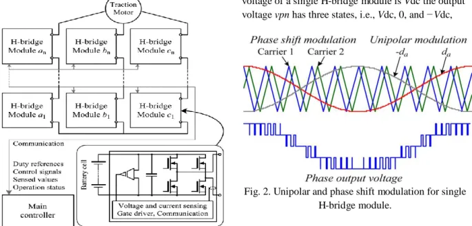
Fig.1. MLCI-based inverter for EV traction drive.
II.SYSTEMCONFIGURATION AND VOLTAGE VECTOR SPACE ANALYSIS
A. Configuration of MLCI for EV Traction Motor Drive
Fig. 1 shows the EV traction motor drive system that is dealt Within this paper. In this configuration, various power ratings can be easily implemented by configuring the number of the single H-bridge modules according to a required specification Such as a neighborhood EV, full-size sedan, and so on. Here each H-bridge module incorporates voltage and current sensing circuitries, gate drivers, and communication interfaces between the module itself and the main controller. In addition, battery cells can be also included in the H-bridge module.
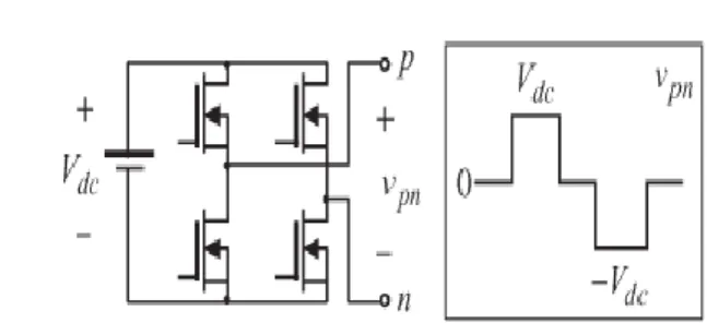
The unipolar modulation technique is applied between two switching legs in the H-bridge module. Consequently, the effective switching frequency in each H-bridge module is twice the carrier frequency. In addition to this, the well-known PS modulation technique is Used to implement interleaving and multilevel operation. Therefore, the effective switching frequency fsw in a phase is
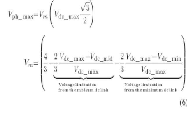
where N and fc represent the number of the H-bridge modules in each phase and the carrier frequency of PWM, respectively. As an example, Fig. 2 shows the carriers for each module, the duty cycles in unipolar modulation, and the output voltage When N = 2. B. Voltage Vector Space Analysis When the dc-link voltage of a single H-bridge module is Vdc the output voltage vpn has three states, i.e., Vdc, 0, and −Vdc,
www.ijseat.com Page 1316 Fig.3.Output voltage of a single H-bridge module.
Fig.4.One-by-three configuration MLCI.
as shown in Fig. 3. By adopting the concept of a switching Function, it can be represented as
where Sp is a switching function and p can be
replaced with a,b, or c, which represent the phases. Fig. 4 shows a simple one-by-three configuration MLCI. For voltage vector space analysis, the main concept is derived from this simple topology, and then, it is expanded to more levels. In Fig. 4, there are two neutral points s and n in the MLCI. Here, the voltage between the output point of each phase and the neutral point n is defined as the pole voltage. The pole voltages are represented as van,
vbn, and vcn. The voltage between the output point of
each phase and the load side neutral point s is Specified as the phase voltage. The phase voltages include vas,vbs, and vcs.
By using this concept, the voltage between the two neutral points is defined as vsn and can be
written as
By using the condition that the sum of all phase voltages is zero because the load does not have a neutral line, vsn is rewritten as
Fig.5. Voltage vector space of one-by-three configuration MLCI.
By substituting (4) into (3), the phase voltage of each phase is represented as follows by using the relationship defined in (2):
If the magnitudes of three dc links are balanced so that Vdc_a, Vdc_b, and Vdc_c have the
same value Vdc, the voltage vector space in α−β
coordinates is defined in Fig. 5(a) by using (5). In the figure, underbars indicate that the switching function has the value of −1. A part of the hexagon in Fig. 5(a) is shown in Fig. 5(b). In this figure, the vectors v010
and v111 are placed at the same reference axis, phase
b. However, the constituents of those vectors are different. For v010, this vector can be synthesized
www.ijseat.com Page 1317 v111 cannot be produced without other vectors
according to (5).
From this, let the vectors which do not require other two phases’ assistance to be defined as ―the independent vectors.‖ Similarly, the vectors which require other phases’ support are defined as ―the dependent vectors.‖ According to these definitions, v100, v001, and v010 are the independent
vectors, while v111, v111, and v111 are the dependent
vectors in Fig. 5(b). Fig. 5(a) also compares the regions that can be composed by the independent. Here, the maximum amplitude of the phase voltage Vph_max in the linear modulation range is defined
Where Vdc_max, Vdc_mid, and Vdc_min represent the
maximum, medium, and minimum voltages among the dc links.
In fact, (6)can be simplified as
It should be noted that Vph_max is the maximum
synthesizable voltage in the linear modulation range in the MLCI undergoing unbalanced dc-link conditions. From (7), it can be recognized that Vph_max is determined by Vdc_mid and Vdc_min. If all
dc links are well balanced so that Vdc_mid and Vdc_min
have identical values, (7) is rewritten as
This is exactly double the maximum synthesizable voltage in the linear modulation range of a traditional three-phase half bridge inverter. In fact, the inverter in Fig. 4 is considered as a three-phase full-bridge inverter which is fed by independent dc links. To extend the proposed approach to the multistage MLCI using PS modulation, the total dc-link voltage per phase is represented as
Where p represents a certain phase among phases a, b, and c, N is the number of the power stage modules in each phase, and j represents the index of a power stage module in each phase. In the multistage MLCI, (9) is utilized to obtain Vdc_max,
Vdc_mid, and Vdc_min. After that, (7) is still applied.
III. NUTRAL VOLTAGE MODULATION TECHNIQUE
In Section II, the maximum synthesizable voltage in the linear modulation range was evaluated under the unbalanced dc links. In this section, a method is proposed to realize the maximum modulation index in the linear modulation range under these conditions.
A. Traditional Offset Voltage Injection Method The offset voltage injection scheme is a popular technique in three-phase half-bridge inverter applications. The theory behind this is that an offset voltage is incorporated with phase voltage
Fig. 6. Implementation of the NVM method.
references to implement various PWM schemes in carrier-based PWM by using the fact that line-to-line voltages are applied to a three-phase load. For example, the offset voltage v∗sn is injected to the
phase voltage references v∗as, v∗bs, and v∗cs
to implement carrier-based SVPWM as in
Then, the pole voltage references v∗an, v∗bn, and v∗cn,
which will be converted to PWM duty references, are
www.ijseat.com Page 1318 B. Proposed NVM Method
If the dc links in an MLCI are unbalanced and the traditional offset voltage injection methods are utilized, the three-phase output voltages may become distorted as the phase voltage reference approaches Vph_max. This is because the traditional
methods are not considering unbalanced dc-link conditions. Therefore, even if a phase can synthesize an output voltage reference in the linear modulation range, the other phases can be saturated or go into the over modulation region. In this situation, a neutral voltage can be produced by the saturated or over modulated phase. In order to resolve this issue and to synthesize the output voltage to Vph_max in the linear
modulation range, the NVM technique is proposed in this paper. Fig. 8 shows the concept of the proposed NVM technique. Here, a neutral voltage between the two neutral points n and s in Fig. 4 is modulated to compensate the output voltage imbalance caused by unbalanced dc-link conditions. To do this, first, the weight constant Kw is defined as
By using (12), the weight factors are calculated as
where Kw_a, Kw_b, and Kw_c represent the weight
factors for phases a, b, and c, respectively. Next, the weight factors are multiplied by the phase voltage references, and the newreferences v_as, v_bs, and v_cs
are obtained as
It should be noted that, depending on dc-link conditions, the sum of v_as, v_bs, and v_cs may not be
zero. By using these components, the injected voltage v_sn and the pole voltage References are given as
From (15), the line-to-line voltages across each phase of theload are represented as
As it can be seen in (16), v_sn does not appear in the
line-to line voltages, and it is still considered as a hidden freedom of voltage modulation. Now, let us consider the role of the weight factors Kw_a, Kw_b,
and Kw_c, which are inversely proportional to the
corresponding dc-link voltage. For convenience, let us assume that the magnitudes of the dc-link voltage are under the following relationship:
Then, from (13) and (17)
Equation (18) gives
From (15) and (19), it can be recognized that, if v_ as, whose dc-link voltage is less than the others, is
corresponding to v_max or v_min, the absolute value of v_sn is greater than vsn in (10).
On the other hand, the final pole voltage references van, vbn, and vcn are calculated by
subtracting v_sn from the original phase voltage
references vas, vbs, and vcs as in (15). From this
reasoning, in this example, it is supposed that, if v_as is corresponding to v_max, then the final pole voltage references van,vbn, and vcn are less than the original pole voltage referencesWithout vsn.
(I) Traditional carrier-based SVPWM. (II) Proposed NVM with Vdc_a = 0.275
Vdc,
Vdc_b = Vdc, and Vdc_c = Vdc.
(III) Proposed NVM with Vdc_a = 0.2 Vdc, Vdc_b = Vdc, and Vdc_c = Vdc. which are not considering v_sn but v∗sn.
Fig.7. Comparison of modulated waveforms.
On the contrary, if v_csis v_max, then the
www.ijseat.com Page 1319 other phases. However, as it can be seen in (16), v_sn
does not affect the line-to-line voltages. Therefore, the line-to-line voltage is the same as the one derived from the original phase voltage reference. From this analysis, the proposed method enables the maximum synthesizable modulation index in the linear modulation range under the unbalanced dc-link conditions to be achieved. In addition to this, if all of the dc-link voltages are well balanced so that Vdc_a,
Vdc_b, and Vdc_c are equal to Vdc
By substituting (20) into (12)–(14)
Equation (21) shows that the proposed method gives the same voltage references as the traditional method under balanced dc-link conditions.
C. Constraints of the Proposed Method
In this section, the limitation of how unbalanced dc links can be while still being compensated by the proposed method is evaluated. Fig. 9 shows the modulated voltage waveforms with different modulation methods and dc-link conditions. In the figure, cases I and II show the results of traditional sinusoidal PWM (SPWM) and carrier-based SVPWM, while cases III and IV illustrate the waveforms of the proposed method with different ratios of dc-link voltages. The fundamental idea to examine the limitation of the proposed method is to evaluate what conditions bring the different polarities between the original voltage reference and the modified voltage reference by using the proposed method. In Fig. 7, the vertices at π/2 and 3π/2 rad almost come in contact with, but do not cross, the zero point. However, the directions of the vertices are opposite the original phase voltage reference in case IV. This means that an excessive and unnecessary voltage is injected into the system. As a result,
Fig.8. Comparison of the duty references and the carriers.
the maximum linear modulation range is reduced, and the line to- line voltage may be distorted. With this basic concept, it is assumed that a phase which has the lowest dc-link voltage commands v∗max and a
phase which has the highest dc-link voltage commands v∗ min to examine a worst case situation.
From (14) and (15), the following equations can be established:
By using (22), the pole voltage reference which is considered as the worst case is
By substituting (22) into (23), we have
Fig.12. Simulation result of SPWM, three-phase voltage references are not zero simultaneously, near a positive peak of the original voltage reference, the sufficient condition which guarantees the same polarity between vmax and vmin is established as follows:
www.ijseat.com Page 1320 Here, it is obvious that k2 is always positive.
Therefore, as long as k1 is positive, the condition (26)
is always satisfied, and k1 can be rearranged as
follows:
Equation (28) is then directly obtained from (27) to ensure that k1 will always be positive
Note that (28) is a sufficient condition to meet the conditions in (25) so that the proposed method can be applied. However, even if (28) is not satisfied so that k1 is negative, there still is a chance to apply the
proposed method. To deal with this situation, let us consider the relationship between v∗max and v∗min as
follows at a positive peak point:
By substituting (29) into (26), we have
Since k1 is negative in this case, the following
condition is derived from (30);
If the relationship between k1 and k2 is established as
in (31), even if the provision in (28) is broken, the conditions in (25) are satisfied so that the proposed method can be still effective. Let us recall Fig. 7 again here. In the figure, the values of |k1| and k2/2
for case III are evaluated as 0.1591 and 0.1593, respectively. Although the difference between the two values is very small, (31) is still true with these values. For case IV, the values of |k1| and k2/2 are
calculated as 0.5 and 0.3, respectively. In contrast to case III, (31) is no longer satisfied, and the directions of the vertices are opposite, as explained previously. From the analysis in this section, both the methods in are successfully able to judge the availability of the proposed method. In terms of accuracy, the latter may give better results. However, in practice, the former may be useful to judge the operation of the proposed method because it is already dealing with an extremely worst case on its own and the calculation in real time is much simpler than (31).
D. Duty Calculation
The final voltage references are entered to the duty reference calculation block. In this block, the duty references of each H-bridge module are calculated as follows:
The calculated duty references are compared to PS carriers to generate gating signals, as shown in Fig. 8. It should be noted that the duty references for each H-bridge in each phase are shared in the PS modulation.
IV.SIMULATION MODEL OF PWM STAREGY BASED MULTILEVEL INVERTER
Fig.9.Simulink Model of Multilevel Cascaded Inverter
www.ijseat.com Page 1321 Fig.11.Control Module of Cascade Inverter
V.SIMULATION RESITS OF MULTILEVEL CASCADED INVERTER
1. SPWM BASED INVERTER
Simulation results of SPWM based multilevel cascaded inverter is as shown fig.12 and %THD of current and voltages as shown in fig.13 & fig.14.
Fig.12. Simulation Result of Traditional SPWM
Fig.13. %THD at Output Current
Fig.14. %THD at Output Voltage
2. SVPWM BASED INVERTER
Simulation results of SPWM based multilevel cascaded inverter is as shown fig.15 and %THD of current and voltages as shown in fig.16 & fig.17.
Fig.15. Simulation Result of Traditional SVPWM
www.ijseat.com Page 1322 Fig.17. %THD at Output Voltage
3. NVM BASED INVERTER
Simulation results of SPWM based multilevel cascaded inverter is as shown fig.18 and %THD of current and voltages as shown in fig.19 & fig.20
Fig.18. Simulation Result of Traditional NVM
Fig.19. %THD at Output Current
Fig.20. %THD at Output Voltage
VI. PROPOSEDPASSIVE LC FILTER BASED INVERTER
Passive LC filer is connected to compensate the harmonics present in inverter output voltage and current. We are placing LC filters with parameter values of L=20mH and C=0.5F
Fig.21. Simulink Model of Passive LC Filter Connected Inverter
www.ijseat.com Page 1323 Fig.23. Simulation Result of NVM for LC Filter
Based Inverter
Fig.24. %THD at Output Current
Fig.25. %THD at Output Voltage
TABLE I
%THD COMPARISONS OF CONTROL STRATEGIES
VII. CONCLUSION
The NVM technique for LC filter based MLCIs under unbalanced dc-link conditions have been proposed in this paper. In order to analyze the maximum synthesizable voltage of MLCIs, the voltage vector space has been analyzed using the switching function. From the analysis, the maximum linear modulation range was derived. The proposed NVM technique is applied to achieve the maximum modulation index in the linear modulation range under an unbalanced dc-link condition as well as to balance the output phase voltages and LC filter network reduces the harmonics present in inverter output voltage and currents. Compared to the previous methods, the proposed technique is easily implemented and improves the output voltage quality under unbalanced dc-link conditions. simulations results based on the IPM motor drive application verify the effectiveness of the proposed method.
REFERENCES
[1] J. Rodriguez, J.-S. Lai, and F. Z. Peng, ―Multilevel inverters: A surveyof topologies, controls, and applications,‖ IEEE Trans. Ind. Electronvol. 49, no. 4, pp. 724–738, Aug. 2002. [2] H. Abu-Rub, J. Holtz, J. Rodriguez, and G. Baoming, ―Medium-voltagemultilevel converters— State of the art, challenges, and requirements in industrial applications,‖ IEEE Trans. Ind. Electron., vol. 57, no. 8, pp. 2581–2596, Aug. 2010.
[3] J.-S. Lai and F. Z. Peng, ―Multilevel converters— A new breed ofpower converters,‖ IEEE Trans. Ind. Appl., vol. 32, no. 3, pp. 509–517,May/Jun. 1996. [4] M. Malinowski, K. Gopakumar, J. Rodriguez, and M. A. Perez, ―A surveyon cascaded multilevel inverters,‖ IEEE Trans. Ind. Electron., vol. 57, no. 7, pp. 2197–2206, Jul. 2010.
[5] J. Rodriguez, L. G. Franquelo, S. Kouro, J. I. León, R. C. Portillo,M. A. M. Prats, and M. A. Perez, ―Multilevel converters: An enablingtechnology for high-power applications,‖ Proc. IEEE, vol. 97, no. 11, pp. 1786–1817, Nov. 2009.
www.ijseat.com Page 1324 [7] Z. Shu, N. Ding, J. Chen, H. Zhu, and X. He,
―Multilevel SVPWM with DC-link capacitor voltage balancing control for diode-clamped multileveconverter based STATCOM,‖ IEEE Trans. Ind. Electron., vol. 60, no. 5,pp. 1884–1896, May 2013.
[8] J. Chavarria, D. Biel, F. Guinjoan, C. Meza, and J. J. Negroni, ―Energybalancecontrol of PV cascaded multilevel grid-connected inverters under
level-shifted and phase-shifted PWMs,‖ IEEE Trans. Ind. Electron., grid-connected converter for renewable distributed systems,‖ IEEE Trans. Ind. Electron., vol. 60, no. 3, pp. 906–918, Mar. 2013. [10] J. A. Munoz, J. R R. Espinoza, C. R. Baier, L. L. Morán, E. E. Espinosa, P. E. Melín, and D. G. Sbárbaro, ―Design of a discrete-time linear control strategy for a multicell UPQC,‖ IEEE Trans. Ind. Electron., vol. 59, no. 10, pp. 3797–3807, Oct. 2012. [11] J. Napoles, J. I. Leon, R. Portillo, L. G. Franquelo, and M. A. Aguirre, ―Selective harmonic mitigation technique for high-power converters,‖ IEEE Trans. Ind. Electron., vol. 57, no. 7, pp. 2315– 2323, Jul. 2010.
[12] L. G. Franquelo, J. Napoles, R. C. Portillo Guisado, J. I. Leon, and M. A. Aguirre, ―A flexible selective harmonic mitigation technique to meet grid codes in three-level PWM converters,‖ IEEE Trans. Ind. Electron., vol. 54, no. 6, pp. 3022–3029, Dec. 2007.
[13] S. Kouro, M. Malinowski, K. Gopakumar, J. Pou, L. G. Franquelo, vol. 60, no. 1, pp. 98–111, Jan. 2013.
[9] G. Buticchi, E. Lorenzani, and G. Franceschini, ―A five-level single-phase and B. Wu, ―Recent advances and industrial applications of multilevel converters,‖ IEEE Trans. Ind. Electron., vol. 57, no. 8, pp. 2553–2580Aug. 2010.
[14] A. M. Massoud, S. Ahmed, P. N. Enjeti, and B. W. Williams, ―Evaluation of a multilevel cascaded-type dynamic voltage restorer employing discontinuous space vector modulation,‖ IEEE Trans. Ind. Electron., vol. 57, no. 7, pp. 2398–2410, Jul. 2010.
[15] M. Hagiwara, K. Nishimura, and H. Akagi, ―A medium-voltage motor drive with a modular multilevel PWM inverter,‖ IEEE Trans. Power Electron., vol. 25, no. 7, pp. 1786–1799, Jul. 2010.
BHARGAVKUMAR.G Completed
B.Tech in Electrical & Electronics Engineering in 2012 from krishna chaitanya institute of technology & sciences,Markapur, Affiliated to JNTU KAKINADA UNIVERSITY, Kakinada and M.Tech in Power Electronic Engineering in 2015 from LENORA COLLEGE Of Engineering, Rampa Chodavaram Affiliated to JNTU KAKINADA UNIVERSITY, Kakinada. Andhra Pradesh, India .Area Of Interest Includes Power Systems & Power Electronics.
DEEPTHIPRIYANKA.S Completed
B.Tech in Electrical & Electronics Engineering in 2008 from VIGNAN Engineering College, Guntur Affiliated to JNTU KAKINADA UNIVERSITY, Kakinada and M.Tech in High Voltage Engineering in 2014 from JNTU Kakinada University Affiliated to JNTU Kakinada. Working as Assistant Professor at LENORA COLLEGE Of Engineering Rampa Chodavaram, Chodavaram Mandal East Godavari, Andhra Pradesh, India. Area of interest includes HVE & Power Electronics.