Multi-Objective CMOS-Targeted Evolutionary Hardware for
Combinational Digital Circuits
Nadia Nedjah and Luiza de Macedo Mourelle
Department of Systems Engineering and Computation, Faculty of Engineering, State University of Rio de Janeiro, Rio de Janeiro, Brazil
E-mail: {nadia, ldmm}@eng.uerj.br
http://www.eng.uerj.br /~ldmm
Key words: Genetic programming, genetic algorithms, evolvable hardware
Received: December 4, 2003
In this paper, we propose a methodology based on genetic programming to automatically generate data-flow based specifications for hardware designs of combinational digital circuits. We aim at allowing automatic generation of balanced hardware specifications for a given input/output behaviour. It minimises space while maintaining reasonable response time. We show that the evolved designs are efficient and creative. We compare them to circuits that were produced by human designers as well as to other evolutionary ones.
Povzetek: Evolucijski algoritem je uporabljen za generacijo specifikacij digitalnih vezij.
1 Introduction
Designing a hardware that fulfils a given function consists of deriving from specific input/output behaviour, an architecture that is operational (i.e. produces all the expected outputs from the given inputs) within a specified set of constraints. Besides the input/output behaviour of the hardware, conventional designs are essentially based on knowledge and creativity. These are two human characteristics too hard to be automated.
The problem of interest consists of designing efficient and creative circuits that implement a given input/output behaviour without much designing effort. The obtained circuits are expected to be minimal both in terms of space and time requirements: The circuits must be compact i.e. use a reduced number of gates and efficient, i.e. produce the output in a short response time. The response time of a circuit depends on the number and the complexity of the gates forming the longest path in it. The complexity of a gate depends solely on the number of its inputs. Furthermore, the design should take advantage of the all the kind of gates available on reconfigurable chip of field programmable gate array (FPGAs).
The three most popular are minimisation techniques are: algebraic method, Karnaugh map [5] and Quine-McCluskeyprocedure [3]. The algebraic method consists of applying some known algebraic theorems and postulates. This method depends heavily on the designer ability, as it does not offer general rules to assist her/him in recognising the theorem to apply. The Karnaugh map [5] is a matrix-based representation of logical functions and allows minimisation of up to 5-input functions. McCluskey procedure [3] is a tabular method and allows one to minimise functions of any number of inputs. Both Karnaugh map and McCluskey procedure produce a minimal sum of products. A combinational circuit based on this minimal form offers the shortest response time,
but not at all the smallest size. However, in some cases, the designer great concern is the minimisation of the number of gates of the circuit as well as the signal propagation delay. Moreover, the McCluskey procedure requires an execution time that grows exponentially with the number of input signals. Furthermore, Karnaugh map and McCluskey procedure produces design that only use AND, OR and NOT gates and ignores all the rest of gates. So the designer needs to perform further refinement on the circuit yield by these methods in order to introduce other kind of gates such as XOR gates [10].
Evolutionary hardware [11] is a hardware that is yield using simulated evolution as an alternative to conventional-based electronic circuit design. Genetic evolution is a process that evolves a set of individuals, which constitutes the population, producing a new population. Here, individuals are hardware designs. The more the design obeys the constraints, the more it is used in the reproduction process. The design constraints could be expressed in terms of hardware area and/or response time requirements. The freshly produced population is yield using some genetic operators such as crossover and
mutation that attempt to simulate the natural breeding process in the hope of generating new design that are
fitter i.e. respect more the design constraints. Genetic evolution is usually implemented using genetic algorithms.
In this work, we design innovative and efficient evolutionary digital circuits. Circuit evaluation is based on their possible implementation using CMOS technology [4], [9]. The produced circuits are balanced
i.e. use a reduced number of gate equivalent and propagate result signals in a reduced response time such that the factor area×performance is minimised. We do so using genetic programming.
genetic programming. In Section 3, we describe the methodology we employ to evolve new compact and fast hardware for a given input/output behaviour. In Section 4, we compare the discovered hardware against existing most popular ones. Finally, we draw some conclusions.
2 Genetic Programming
Genetic programming [6] is an extension of genetic algorithms. The chromosomes are computer programs and the genes are instructions. In general, genetic programming offers a mechanism to get a computer to provide a solution of problem without being told exactly how to do it. In short, it allows one to automatically create a program. It does so based on a high level statement of the constraints the yielded program should obey to. The input/output behaviour of the expected program is generally considered as an omnipresent constraint. Furthermore, the generated program should use a minimal number of instructions and have an optimal execution time.
Starting form random set of computer programs, which is generally called initial population, genetic programming breeds a population of programs through a series of steps, called generations, using the Darwinian principle of natural selection, recombination also called
crossover, and mutation. Individuals are selected based on how much they adhere to the specified constraints. Each program is assigned a value, generally called its
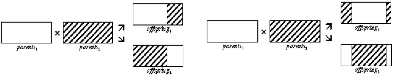
fitness, which mirrors how good it is in solving the program. Genetic programming [6] proceeds by first, randomly creating an initial population of computer programs; then, iteratively performing a generation, which consists of going through two main steps, as far as the constraints are not met. The first step in a generation assigns for each computer program in the current population a fitness value that measures its adherence to the constraints while the second step creates a new population by applying the three genetic operators, which are reproduction, crossover and mutation to some selected individuals. Selection is done with on the basis of the individual fitness. The fitter the program is, the more probable it is selected to contribute to the formation of the new generation. Reproduction simply copies the selected individual from the current population to the new one. Crossover recombines two chosen computer programs to create two new programs using single-point crossover or two-point crossover as shown in Figure 1.
Mutation yields a new individual by changing some randomly chosen instruction in the selected computer program. The number of genes to be mutated is called
mutation degree and how many individuals should suffer mutation is called mutation rate.
3 Evolving Hardware for
Combinational Digital Circuits
There three main aspects in implementation of genetic programming [6], [7]: (i) program encoding; (ii)
crossover and mutation of programs; (iii) program fitness. In this section, we explain how we treat these three aspects in our implementation.
3.1 Circuit Specification Encoding
Encoding of individuals is one of the implementation decisions one has to take in order to use evolutionary computation. It depends highly on the nature of the problem to be solved. There are several representations that have been used with success: binary encoding which is the most common mainly because it was used in the first works on genetic algorithms, represents an individual as a string of bits; permutation encoding
mainly used in ordering problem, encodes an individual as a sequence of integer; value encoding represents an individual as a sequence of values that are some evaluation of some aspect of the problem; and tree encoding represents an individual as tree. Generally, the tree coincides with the concrete tree as opposed to
abstract tree [1] of the computer program, considering the grammar of the programming language used.
Here a design is specified using register transfer level equations. Each instruction in the specification is an output signal assignment. A signal is assigned the result of an expression wherein the operators are those that represent basic gates in CMOS technology of VLSI circuit implementation and the operands are the input signals of the design. The allowed operators are shown in Table 1. Note that all gates introduce a minimal propagation delay as the number of input signal is minimal, which is 2. A NOT gate inverts the input signal, an and-gate propagates a 1-signal when both input signals are 1 and 0-signal otherwise and an or-gate propagates a 0-signal when both input signals are 0 and 1-signal otherwise. An AND gate inverts the signal propagated by a NAND gate while an OR gate inverts that
propagated by a NOR gate. Note that, in CMOS technology, an and-gate is a NAND gate coupled with a NOT gate and an OR gate is a nor-gate followed by a not-gate and not the inverse [4]. The XOR gate is a CMOS basic gate that has the behaviour of sum of products
y x y
x + wherein x and y are the input signals. However,
a XOR gate is not implemented using 2 AND gates, 2 NOT gates and an OR gate. A 2to1-multipliexer MUX is also a CMOS basic gate and implements the sum of products
ys s
x + wherein x and y are the first and the second input signals and s is the control signal. It is clear that a XOR and MUX gates are of the same complexity [4], [9].
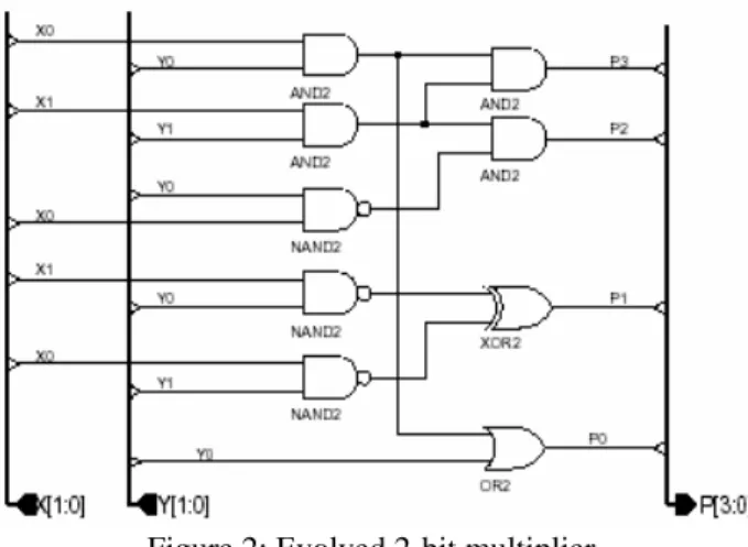
For instance, a 2-bit multiplier has 4-bit result signal so an evolved register transfer level specification is as follows, wherein the input operands are X =<x1x0> and Y
=<y1y0> and the output is the product P =<p3p2 p1p0>.
p3 ⇐ (x0ANDy0) AND (x1ANDy1)
p2 ⇐ (x0NANDy0) AND (x1ANDy1)
p1 ⇐ (x1NANDy0) XOR (x0NANDy1)
p0 ⇐ (y0ANDx0) ORy0
The schematic of the digital circuit implementing the above specification is given in Figure 2.
Figure 2: Evolved 2-bit multiplier
We encode specifications using an array of concrete trees corresponding to its signal assignments. The ith. tree
represents the evaluation tree of the expression on the left-hand side of the ith. signal assignment. Leaf nodes are labelled with a literal representing a single bit of an input signal while the others are labelled with an operand. The individual corresponding to above specification is shown in Figure 3.
Figure 3: Chromosome for the evolved 2-bit multiplier
3.2 Circuit Specification Reproduction
Crossover of circuit specification is implemented using a double-point crossover as described in Figure 1. One of the important and complicated operators for genetic programming is the mutation. It consists of changing a gene of a selected individual. The number of individuals that should suffer mutation is defined by the mutation rate while how many genes should be altered within a chosen individual is given by the mutation degree.
Here, a gene is the tree of the expression on the left hand side of a signal assignment. Altering an expression can be done in two different ways depending on the node that was randomised and so must be mutated. A node represents either an operand or operator. In the former case, the operand, which is a literal representing a bit in the input signal, is substituted with either a literal or
simple expression. The decision is random. In the case in which the operand has to be changed by another operand, the literal representing the bit of lesser significance in the binary notation of the input signal or that representing its most significant bit is used. This is performed as indicated by function mutate1 below, wherein X =<xn−1x
n−2 … x1x0> is the signal obtained by the concatenation of
all input signals:
⎪ ⎩ ⎪ ⎨
⎧ =
=
− −
otherwise 0
) (
1 1
1
i n i
x
i x
x mutate
Name Symbol Name Symbol
NOT NAND
AND NOR
OR XNOR
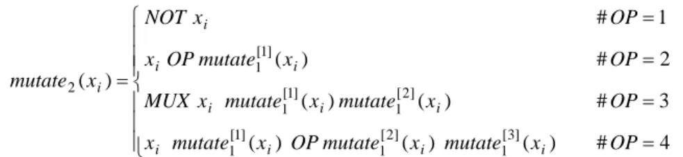
XOR MUX
In the case of mutating an operand node to an operator node, we proceed as follows: First let xibe the operand being mutated. We choose randomly an operator among those available. Let OP be this operator. Its first operand is xi. So if the chosen operator is NOT then the operand node is mutated to NOT xi. When the selected operator is binary, a new literal is generated using mutate1(xi). Thus, in this case, xi is mutated to either xi OP mutate(xi), wherein OP is an available binary operator. If the chosen operator is MUX, then a third operand is generated using
mutate1(mutate1(xi)). Last but not least, when the selected operator is quaternary a fourth literal is generated in the same way, i.e. using mutate1(mutate1(mutate1(xi))). This mutation procedure is implemented by function mutate2
below wherein the notation mutate1[i](x) represents the i
times application of mutate1 and #OP represents the arity of operator OP:
So far we explained how an operand node is mutated. Now, we describe the mutation process of an operator node. Let OP be the operator being changed. An operator node can be mutated to another operator node or to an operand node. In the latter case, a literal is randomised and used to substitute the operator node. In the former case, however, things become a little more complicated depending on the relation between the arity OP and that of the operator selected to substitute it, say OP′. So we mutate OP to OP′. When #OP = #OP′ we leave the operands unchanged. Note that this case happens only for binary and quaternary operators. When #OP > #OP′, we use only a random subset of OP’s operands. Finally, i.e. when #OP < #OP′, we generate a random set of literals using function mutate1 repetitively as in function mutate2
above. Note that, the last case can occur for NOT, MUX and binary operators but not for quaternary operators.
3.3 Circuit Specification Evaluation
Another important aspect of genetic programming is to provide a way to evaluate the adherence of evolved computer programs to the imposed constraints. In our
case, these constraints are of three kinds. First of all, the evolved specification must obey the input/output behaviour, which is given in a tabular form of expected results given the inputs. This is the truth table of the expected circuit. Second, the circuit must have a reduced size. This constraint allows us to yield compact digital circuits. Thirdly, the circuit must also reduce the signal propagation delay. This allows us to reduce the response time and so discover efficient circuits. In order to take into account both area and response time, we evaluate circuits using the area×performance factor. We evolve
balanced digital circuits that implement a given behaviour that require a reduced hardware area and produce the result in a reduced time such that
area×performance factor is minimal.
We estimate the necessary area for a given circuit using the concept of gate equivalent. This is the basic unit of measure for digital circuit complexity [4], [9]. It is based upon the number of logic gates that should be interconnected to perform the same input/output behaviour. This measure is more accurate that the simple number of gates [4].
When the input to an electronic gate changes, there is a finite time delay before the change in input is seen at the output terminal. This is called the propagation delay of the gate and it differs from one gate to another. Of primary concern is the path from input to output with the highest total propagation delay. We estimate the performance of a given circuit using the worst-case delay path. The number of gate equivalent and an average propagation delay for each kind of gate are given in Table 2. The data were taken form [4].
Let C be a digital circuit that uses a subset (or the complete set) of the gates given in Table 2. Let Gates(C) be a function that returns the set of all gates of circuit C
and Levels(C) be a function that returns the set of all the gates of C grouped by level. For instance, applied to the circuit of Figure 2, it returns the set of sets {{AND, AND, NAND, NAND, NAND}, {AND, AND, XOR, OR}}. Notice that the number of levels of a circuit coincides with the cardinality of the set expected from function Levels. On
⎪ ⎪ ⎪ ⎩ ⎪⎪ ⎪ ⎨ ⎧ = = = = = 4 # ) ( ) ( ) ( 3 # ) ( ) ( 2 # ) ( 1 # ) ( ] 3 [ 1 ] 2 [ 1 ] 1 [ 1 ] 2 [ 1 ] 1 [ 1 ] 1 [ 1 2 OP x mutate x mutate OP x mutate x OP x mutate x mutate x MUX OP x mutate OP x OP x NOT x mutate i i i i i i i i i i i
Name Gate equivalent
Propagation
delay (ns) Name
Gate equivalent
Propagation delay (ns)
NOT 1 0.0625 NAND 1 0.13
AND 2 0.209 NOR 1 0.156
OR 2 0.216 XNOR 3 0.211
XOR 3 0.212 MUX 3 0.212
the other hand, let Value(T) be the Boolean value that the considered circuit C propagates for the input Boolean vector T assuming that the size of T coincides with the number of input signal required for circuit C. The fitness function, which allows us to determine how much an evolved circuit adheres to the specified constraints, is
given as follows, wherein In represents the input values of the input signals while Out represents the expected output values of the output signals of circuit C, n denotes the number of output signals that circuit C has and function Delay returns the propagation delay of a given gate as shown in Table 2.
∑
∑
∑
∑
∈ ∈ ∈ = ≠×
+
⎟
⎟
⎠
⎞
⎜
⎜
⎝
⎛
=
) ( ) (1 ( []) [,]
)
(
)
(
)
(
C LevelsL g L
C Gates g n
j iValueIni Outij
g
Delay
Max
g
lent
GateEquiva
Penalty
C
Fitness
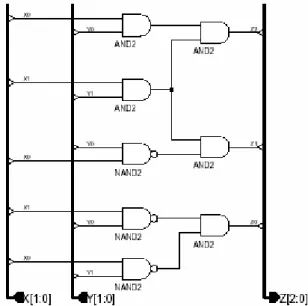
For instance, consider the evolved circuit of Figure 4. It should propagate the output signals of Table 3 that appear first (i.e. before symbol /) but it actually propagates the output signals that appear last (i.e. those after symbol /). Observe that signals Z2 and Z1are correct for every possible input combination of the input signals. However, signal Z0 is correct only for the combinations 1010 and 1111 of the input signals and so for the remaining 14 combinations, Z0 has a wrong value and so the circuit should be penalised 14 times. Applying function Gates to this circuit should return 5 AND gates and 3 NAND gates while function Levels should return {{AND, AND, NAND, NAND, NAND}, {AND, AND, AND}}. If penalty is set to 10 then, function Fitness should return 140 + (5×2+3×1) × (0.209+0.209). This fitness sums up to 145.434.
Figure 4: Evolved circuits for example 1
Note that for a correct circuit the first term in the definition of function Fitness is zero and so the value returned by this function is the factor area×performance of the evaluated circuit.
In order to speed up the computation of the evolved circuit fitness, we take advantage of the parallelism of the central processing unit. This technique was first used by Poli in [8]. Instead of obtaining the output signal values one by one, one can compute them i.e. for all possible input signal combinations, in parallel. For instance, to compute the values of output signal Z2 <= (X0
AND Y0) AND (X1 AND Y1) considering the circuit of
Figure 4 and the values of Table 3, we proceed as follows:
X1 X0 Y1 Y0 Z2 Z1 Z0 0 0 0 0 0/0 0/0 0/1 0 0 0 1 0/0 0/0 0/1 0 0 1 0 0/0 0/0 0/1 0 0 1 1 0/0 0/0 0/1 0 1 0 0 0/0 0/0 0/1 0 1 0 1 0/0 0/0 0/1 0 1 1 0 0/0 0/0 1/0 0 1 1 1 0/0 0/0 1/0 1 0 0 0 0/0 0/0 0/1 1 0 0 1 0/0 0/0 1/0 1 0 1 0 0/0 1/1 1/1 1 0 1 1 0/0 1/1 1/0 1 1 0 0 0/0 0/0 0/1 1 1 0 1 0/0 0/0 1/0 1 1 1 0 0/0 1/1 1/0 1 1 1 1 1/1 0/0 0/0
Table 3: Truth table of example 1
1. Convert 0000111100001111, which is the content of
column X0 to integer value 3855 and
0101010101010101, which is the content of column
Y0 to integer value 21845;
2. Compute the bitwise operation 3855 & 21845 = 1285;
3. Convert 0000000011111111, which is the content of
column X1 to integer value 255 and
0011001100110011, which is the content of column
Y1 to integer value 13107;
4. Compute the bitwise operation 255 & 13107 = 51; 5. Compute the bitwise operation 1285 & 51 = 1;
6. Convert 1 to its 16-bit binary representation 000000000000001, which is exactly the content of column Z2.
4 Evolutionary vs. Conventional
Designs
In this section, we compare the evolutionary circuits yield by our genetic programming based evolution to those designed by a human as well as to those evolved by Coelho’s genetic algorithm [2].
The truth table of the first example is given in Table 4. It has three-bit input signal X = <x2x1x0> and propagates a single-bit output signal Y.
X2 X1 X0 Y
0 0 0 0 0 0 1 0 0 1 0 0 0 1 1 1 1 0 0 0 1 0 1 1 1 1 0 1 1 1 1 0
Table 4: Truth table of example 1
For example 1, a human designer came with a digital circuit that uses 2 AND gates, 1 OR gate and 2 XOR gates. The output signal is computed as in signal assignment (1). The Coelho’s genetic algorithm evolved the circuit specified in signal assignment (2). It uses 1 XOR gate less than the human designed circuit.
Y⇐x0AND (x2XORx1) ORx1AND (x2XOR x0) (1)
Y⇐x0AND (x2ORx1) XOR (x2AND x1) (2)
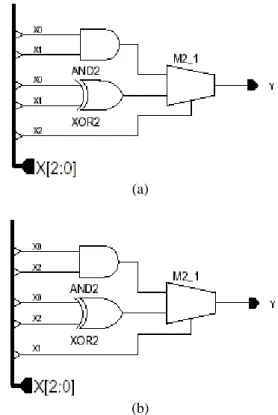
Our genetic programming based evolutionary computation yield two different circuits for example 1. Both of them use 1 AND gate, 1 XOR gate and 1 MUX
gate. The specifications of theses two circuits are given in signal assignment (3) and (4) respectively:
Y⇐MUX((x0ANDx1), (x0XORx1), x2) (3)
Y⇐MUX((x0ANDx2), (x0XORx2), x1) (4)
The schematics of these two circuits are given in Figure 5. The circuit, we evolved needs less hardware area, propagates the output signal faster and so the factor
area×performance is minimised. The numerical figures are given in Table 6.
(a)
(b)
Both examples 2 and 3 need a 4-bit input signal X = <x3x2x1x0> and yield a single-bit output signal Y. Examples 4 and 5 also requires a 4-bit input signal X but the respective circuits must propagate a 4-bit and 3-bit output signal respectively. The truth tables of four examples are summarised in Table 5 below. Note that example 4 is a simple 2-bit multiplier of X = <x3x2> times Y = <x1x0> (notation for space sake).
For the second example, a human designer came with a circuit that requires 4 AND gates, 1 OR gate, 2 XOR gates and 4 NOT gates. The specification of the signal assignment (5) is as follows:
Y ⇐ ((x3ANDx1) XOR (x0AND x2 )) OR ((x1ANDx0)
AND (x3XOR x2 )) (5)
For example 2, the Coelho’s genetic algorithm evolved the circuit specified in signal assignment (6). It uses 1 AND gate, 3 OR gates, 3 XOR gates and 1 NOT gate.
Y ⇐ ((x3 XOR ((x2XOR x0) OR (x1 ANDx0)) XOR (NOT ((x3
OR (x1 ORx0))) (6)
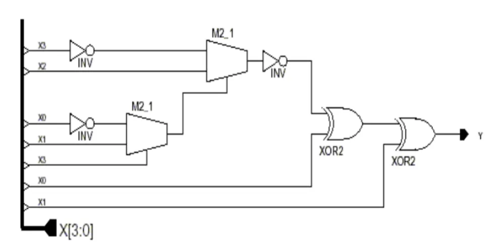
The schematics of the circuit we evolved are given in Figure 6. It needs less hardware area, but propagates the output signal a little bit slower than Coelho’s evolved circuit. However, the factor area×performance is the smallest. Again, the numerical figures are given in Table 6.
Figure 6: Evolved circuits for example 2
For the third example, a human designer obtained a circuit that requires a total of 20 gates equivalent: 5 AND gates, 3 OR gates and 4 NOT gates. The specification of the signal assignment (7) is as follows:
Y ⇐ ((x3AND x0) OR (x0AND x2 )) OR ((x2 ANDx1)
OR (x3AND x1 AND x0)) (7)
Input Examples 2, 3 Example 4 Example 5
X3 X2 X1 X0 Y Y P3 P2 P1 P0 Y2 Y1 Y0
For example 3, the Coelho’s genetic algorithm evolved the circuit specified in signal assignment (8). It requires 2 AND gates, 2 OR gates, 2 XOR gates and 1 NOT gate.
Y ⇐ NOT(((x2 ANDx1) XOR (x2 OR x0)) AND (x1 OR (x3
XORx0))) (8)
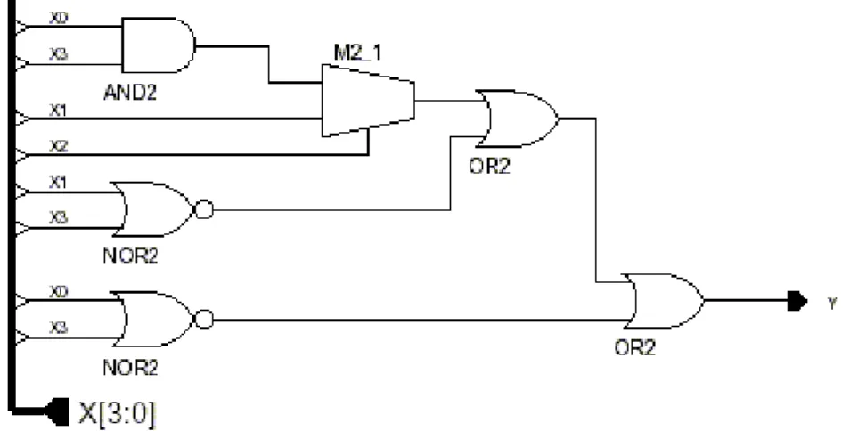
The schematics of the circuit we evolved are given in Figure 7. The circuit, we evolved needs less hardware area, propagates the output signal faster than both circuits i.e. Coelho’s and the one designed by the human, and so the factor area×performance is minimised. Once more, the numerical figures about gate equivalent, delay and
area×performance factor are shown in Table 6.
Figure 7: Evolved circuits for example 3
Another circuit was obtained for example 3. Its schematics are given in Figure 8 below. The circuit of Figure 8 is less efficient than that shown in Figure 7. However, it is more compact that the circuits obtained by the human designer and that evolved by Coelho’s genetic algorithm as it requires only 11 gates equivalent
compared to 20 for the circuit designed by the human and 15 for Coelho’s evolved circuit. Moreover, the circuit of Figure 8 has a smaller propagation delay of 0.853ns compared to the 0.912ns required by the human designed circuit. The circuit presents a
area×performance factor of 9.383.
Figure 8: Less efficient evolved circuits for example 3
For the fourth example, a human designer obtained a circuit that requires a total of 24 gates equivalent: 8 AND gates, 2 OR gates, 1 XOR gate and 1 NOT gate. The specification of the signal assignments is as follows, wherein y1 = x3 and y0 = x2 when Table 5 is used.
p0 ⇐ (x0ANDy0)
p1 ⇐ (x1ORx0) AND (y1ORy0) AND ((x1ANDx0) XOR (y1
ANDy0))
p2 ⇐ (x1ANDy1) AND NOT((x0ANDy0))
p3 ⇐ (x1ANDy1) AND (x0ANDy0)
For example 4, the Coelho’s genetic algorithm evolved the circuit specified in the following output signal assignments. It requires an area of 16 gates equivalent. That is 5 AND gates and 2 XOR gates.
p1 ⇐ (x0ANDy1) XOR (x1ANDy0)
p2 ⇐ (x1ANDy1) XOR ((x0ANDy0) AND (x1ANDy1))
p3 ⇐ (x1ANDy1) AND (x0ANDy0)
The schematics of the circuit we evolved are given in Figure 9. The circuit, we evolved needs the same
hardware area as Coelho’s evolved circuit but it propagates the output signal faster than both circuits i.e. Coelho’s and the one designed by the human, and so the factor area×performance is minimised. The comparison of the numerical figures such as gate equivalent numbers, propagation delays and area×performance factors is detailed in Table 6.
Figure 9: Evolved circuits for example 4
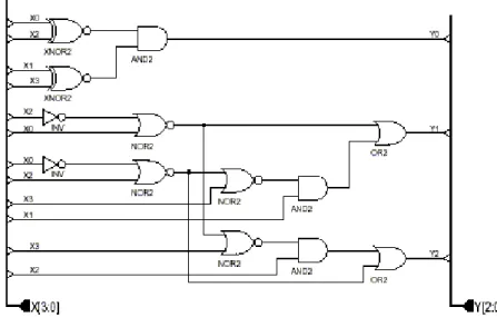
Finally for the fifth example, a human designer engineered a circuit that requires a total of 34 gates equivalent, i.e. 7 AND gates, 4 OR gates, 2 XOR gate and 6 NOT gates. The specification of the signal assignments is as follows, wherein y1 = x3 and y0 = x2 when Table 5 is used.
y0 ⇐ NOT (x3XORx1) ANDNOT (x2XORx0)
y1 ⇐ (x2 ANDx0) AND (x3ORx1) OR (x3ANDx1)
y2 ⇐ (x0ANDx2) AND (x1ORx3) OR (x1ANDx3)
For the same example, the Coelho’s genetic algorithm evolved the circuit specified in the following output signal assignments. It requires an area of 22 gates equivalent, which consist of 2 AND gates, 3 OR gate, 3 XOR gates and 3 NOT gates.
y0 ⇐ NOT ((x3XORx1) AND (x2XORx0))
y1 ⇐ tempANDNOT (((x3XORx1) AND x3XOR (x0OR (x3
XORx1))) OR temp)
y2 ⇐ NOT (((x3XORx1) AND x3XOR ((x0OR (x3XORx1)) OR NOTtemp)
wherein temp = ((x2 XORx0) OR (x3XORx1)).
The schematics of the circuit that our genetic algorithm evolved are given in Figure 10. This circuit requires one gate equivalent more than Coelho’s evolved circuit but our circuit propagates the output signal much faster. Compared with the human designed circuit, our circuit has the same response time but needs a much smaller area. Furthermore, the factor area×performance
for our circuit is minimal compared with the other two. The numerical figures such as gate equivalent numbers, propagation delays and area×performance factors are given in Table 6.
Figure 10: Evolved circuits for example 5
0 20 40 60 80 100 120 140 160 180 200
0
50
100 150 200 250 300 350 400 450 500 550 600
#generation fitness
1st. Benchmark 2nd. Benchmark 3rd. Benchmark 4th. Benchmark 5th. Benchmark
Figure 11: Convergence graphs for the evolution of the circuits of the five examples
In order to evolve the circuits for the proposed behaviours (see Table 5) and for all of the examples we used a population of 100 individuals. The double-point crossover was used with mutation rate of 0.5 and a mutation degree of 1.
Table 6 shows a comparison between the fittest circuits engineered by a human designer, Coelho’s
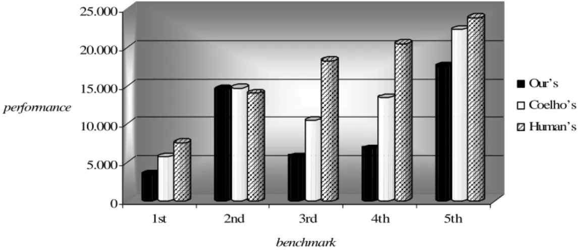
genetic algorithm and our genetic algorithm, which is based on genetic programming. For each proposed example, the required hardware area, the necessary propagation delay and the product area×performance are detailed. The graphical representation of these figures is shown in the chart of Figure 12.
area delay area×performance
Our’s Coelho’s Human’s Our’s Coelho’s Human’s Our’s Coelho’s Human’s
1st 8 9 12 0.424 0.637 0.637 3.392 5.733 7.644
2nd 15 16 20 0.973 0.918 0.702 14.595 14.696 14.050
3rd 9 15 20 0.639 0.699 0.912 5.751 10.492 18.250
4th 16 16 24 0.425 0.842 0.853 6.800 13.472 20.472
5th 22 21 34 0.799 1.065 0.703 17.589 22.365 23.919
0 5.000 10.000 15.000 20.000 25.000
performance
1st 2nd 3rd 4th 5th
benchmark
Our’s Coelho’s Human’s
Figure 12: Graphical comparison of the area×delay factor
5 Conclusions
In this paper, we described an evolutionary technique to engineer compact, efficient and creative digital combinational circuit given the expected input/output behaviour. We explored the use of genetic programming and changing from the binary representation of circuits to a tree representation. We showed how to improve the evolution process by taking advantage of the central processing unit parallelism. An advantage of using genetic programming consists of the readability of the evolved circuit for synthesis using one of the available synthesis tools [12].
Our evolutionary process is multi-objective as it allows one to yield balanced i.e. compact and efficient digital circuits. The proposed fitness function evaluates a given circuit with respect to correctness, required hardware area and necessary propagation delay of output signals. It does so using the well-agreed-upon factor
area×performance as a measure to appreciate the complexity of a digital circuit.
We evolved a better circuit for every example used by Coelho et al. [2] compared to both human designs and evolved circuit that only consider the number of required gates to evaluate an evolved solution. On one hand, this proves that the fitness function we engineered is far more realistic than that of used by Coelho et al. On the other hand, it also proves that evolutionary hardware can offer an alternative way to human design techniques to design efficient digital circuit. We showed how the evaluation of circuit fitness can be computed efficiently taking advantage of the inherent parallelism of the central processing units of the computers.
References
1. A.V. Aho, S. Ravi and J.D. Ullman, Compilers: principles, techniques and tools, Addison-Wesley, 1986.
2. A.A.C. Coelho, A.D. Christiansen and A.H. Aguirre, Towards Automated Evolutionary Design of Combinational Circuits, Comput. Electr. Eng., 27, pp. 1-28, 2001
3. E.J. McCluskey, Minimisation of Boolean
functions, Bell Systems Technical Journal, 35(5):1417-1444, November 1956.
4. M.D. Ercegovac, T. Lang and J.H. Moreno,
Introduction to digital systems, John Wiley, 1999.
5. M. Karnaugh, A map method for synthesis of
combinational logic circuits, Transactions of the AIEE, Communications and Electronics, 72 (I):593-599, November 1953.
6. J. R. Koza, Genetic Programming. MIT Press, 1992.
7. J.F. Miller and D. Job, Principles in the
evolutionary design of digital circuits
8. R. Poli, Efficient evolution of parallel binary multipliers and continuous symbolic regression expressions with sub-machine code GP, Technical Report CSRP-9819, University of Birmingham, School of Computer Science, December 1998. 9. V.T. Rhyne, Fundamentals of digital systems
design, F.F. Kuo Ed. Prentice-Hall Electrical Engineering Series, 1973.
10. B.C.H. Turton, Extending Quine-McCluskey for exclusive-or logic synthesis, IEEE Transactions on Education, 39(1):81-85, February 1996.
11. A. Thompson, P. Layzel and R.S. Zebelum,
Explorations in design space: unconventional design through artificial evolution, IEEE Transactions on Evolutionary Computations, 3(3):81-85, February 1996.