An Efficient Step-Up Converter with a Low Switch Stress
Van-Tsai Liu
*Department of Electrical Engineering, National Formosa University, Yunlin County, 632, Taiwan
Received 02 July 2012; received in revised form 14 August 2012; accepted 12 September 2012
Abstract
A novel approach is proposed for a high step-up and high efficiency converter with a low switch stress. The
integrated boost-flyback converter uses coupled-inductor techniques to achieve high step-up voltage with low duty
ratio, and thus the slope compensation circuit is disregarded. The proposed circuit topology improving high-gain
ratio,increasing efficiency, reducing the secondary side of copper loss, and having an active-clamp effect that can
reduce the switch stress on power components and have the energy feedback mechanism. Such a method of high
efficiency and simple control can reduce cost which makes production size in increasing demand at present.
Therefore, designing converters becomes a challenge when stepping up voltage with high efficiency and high power
output. This thesis is a design of a high-efficiency step-up converter with low switch stress. The designis simple in
that
Keywords: step-up, low switch stress, active-clamp
the circuit requires only a pulse width modulation (PWM) signal output. In addition, at cut-off time, the MOSFET
generates a spike by way of a circuit sent to the output. This way can achieve the goal of energy recovery, an
active-clamp, and can reduce the switch stress of power switch to improve circuit efficiency. Experimental results
have confirmed that the proposed converter possesses high step-up, high efficiency, and low switch stress.
1.
Introduction
Alternative energy is currently most common in solar energy, wind power, and hydrogen fuel. The Grid-Tie or supply to
high voltage equipment will be a challenge for PV systems, wind generators, and fuel cells to obtain high-voltage solar power
that usually produces a number of solar cells in a series into a large-scale module. Moreover, to achieve high-voltage output, the
number of solar cells in a series must also increase costs. For medium-sized wind power generators and fuel cell which output
voltages are not high, wind power and fuel cells do not apply in a series. Regarding PV systems, wind turbines, and fuel cells as
the power grid or supply to high voltage devices, using DC-to-DC power converters with high step-up is the most favorable
choice. However, this high step-up converter from low voltage input to high voltage output easily leads to problems of
inefficiency. Therefore, how to make good use of PV systems, wind turbines, and fuel cells to reduce costs and improve
efficiencies is the primary focus of this study.
For example, K. C. Tseng [1, 2] of boost-flyback converters combined boost and flyback converters significantly
improves the voltage gain ratio. Additionally,this structure has an active-clamp that can reduce the switch stress of power
devices and energy regeneration mechanisms. This structure also hascontrol of simple, high efficiency, and the secondary side
of the stack that can improve voltage to gain characteristics. Rong-Jong Wai [3-6] enhanced the voltage gain ratio and reduced
the switch stress of power devices based on coupled-inductor technology. Unfortunately, this structure has no boost-flyback
converter secondary side of the stack effect to enhance the voltage gain. Spiazzi G. [7] of circuit structure is similar to the
boost-flyback converter in that the circuit features added a forward converter. However, the circuit for forward and flyback
types of output capacitors connected in a series to the load output causes the output voltage to ripple and the issue of greater for
transformer air gap. Shih-Kuen Chang Chien [8] of circuit structure is similar to [7]. The circuits for forward and flyback type
of output capacitors were connected similarly in a series to the load output, but the circuit structure enhanced the [7] voltage
gain. Suman and Dwari [9] and Wuhua Li [10] of coupled inductor circuit used parallel arrays to improve the voltage gain, and
a phase shift circuit in each group, which can obtain the average input current and reduce the loss of power components.The
disadvantage is that control is not easy, and requires more pulse width modulation signals.
This article focuses on the design of a converter with high efficiency and high step-up. This circuit structure retains
advantages and features of a boost-flyback converter, and increases the voltage gain ratio more effectively. Moreover,
transformer copper loss can be reduced on the secondary side.
2.
People gradually have the environmental awareness and start to use the renewable energy, such as solar power, wind
power, and hydrogen fuel regarding green energy related circuit products and applications which output voltage is not high.
Therefore, these need to use converters with high efficiency, high step-up, and high power. However, for high efficiency, high
gain, and high power converters, the priority is to be designed with relatively high conversion efficiency. The priority has been
compared with the 500-W efficiency in references [11] and [12].However, the output power is larger and has a relatively large
input current and loss of transformer and power components are enhanced. The trend of declining efficiency which in the design
is more difficult to control. What way is necessary for using large heat sinks or cooling means to exclude losses arising from the
heat, which easily create larger product size and weight. Although, the conversion efficiency can be improved by adapting the
design, but now a number of high efficiency, high step-up and high power converter circuit design is very complicated, which is
more control mode that caused by the difficulties of manufacture and its increased costs. To solve the demands of the
conversion circuit that meet high-gain, high performance and design is not simple. For difficulties of design, large size, and poor
efficiency, design costs are higher and yield many technical problems. This article combined with primary side and secondary
side, improve high-gain ratio,increase its efficiency, reduce the secondary side of copper loss, and have having an active-clamp
effect. Such a method which involves high efficiency and simple control can reduce the cost and size of the product.
Design of Circuit
This article describes the design of a high-efficiency step-up converter,which improves [1] can be seen from Fig. 1. This
design has the advantage of low switch stress, high voltage gain, and high power. The proposed converter is shown in Fig. 2. The
proposed step-up converter combined with primary-side and secondary-side. Primary-side having a boost circuit and
secondary-side is used a voltage lift equivalent and flyback circuit to improve the voltage gain and reduce the secondary-side of
C2
C1
N1
N2
S
D1
D2
RL
+
-+
-+
-Vo
Vi
Lm
Fig. 1
D3
VI
C1
RL D2
D1
C2
C3
S N1
N2
VO
Primary Side
Secondary Side
Novel High-Efficiency Step-Up Converter
Fig. 2 Circuit configuration of the
D3
VI
C1 RL
D2
D1 C2
C3
S N1
N2
VO
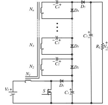
D5 D4 C4
C5 N3
D7 D6 C6
C7 Nn
● ● ●
proposed step-up converter
Fig. 3 Proposed step-up
VI
C1
RL
D2
D1 C2
S N1
N2
VO
D3 C3 N3
D5 D4 C4 Nn
● ● ●
C5
converter with the secondary-side of the series
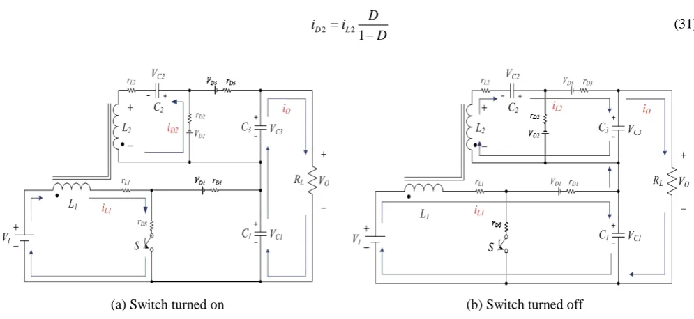
2.2. Working Principle
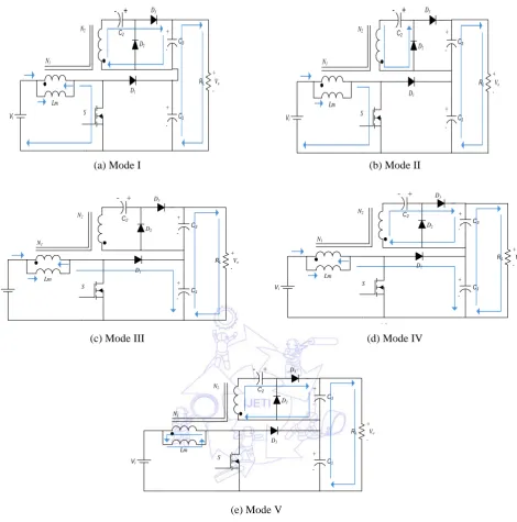
Fig. 5 shows the characteristic waveforms during five operation modes of the proposed converter in one switching period.
The circuit operation mode status is shown in Fig. 6
VGS
VDS
Ii
ID1
ID2
ID3
ILm
t0 t1 t2 t3 t4 t5 t t t t t t t
. The operating principle of continuous-conduction mode for proposed
converter is presented in detail.
Fig. 5 Characteristic waveforms of the proposed converter under CCM operation during one switching period
Mode I [t0, t1]: At t = t0, switch S is turned on. Diode D1 and D2 are turned off and D3
1
i Lm Lk
V =V +V
is turned on. The voltage equation
of the primary-side of coupled inductor is . Simultaneously, the voltage V
N2 is induced. Therefore, the primary-side current of the coupled inductor iLk1 increases linearly and the secondary current is decreases linearly. When
current iN2 becomes zero, diode D3 is turned off. The magnetizing inductor Lm starts to charge by the DC source Viand the
diode D2 starts to turned on. As current iLk1 is equal to iLm+n2⋅iN2 at t = t1
Mode II [t
, this operating mode is ended.
1, t2]: During this time interval, switch S is turned on. Diodes D1 and D3 are turned off, and D2 is turned on. The magnetizing inductor Lm is charged by the DC-source Vi. Meanwhile, on the secondary-side winding N2 of the voltage VN2is
charge to the capacitor C2. Voltage VC2 is approximately equal to nVN2. When current iLk becomes zero, diode D1 is turned on.
This operating mode is ended at t = t2
Mode III [t
.
2, t3]: During this time interval, switch S is turned off. Diodes D1 and D2are turned on and D3 is turned off. The energy of the leakage inductance Lk1 and magnetizing inductor Lm charge to the parasitic capacitor Cds of switch S. Capacitor C2 is charged by VN2. While the capacitor voltage Vds is equal to Vi + VLk1 at t = t3, diode D1
Mode IV [t
conducts and this
operating mode is ended.
3, t4]: At t = t3, switch S is turned off. Diodes D1 and D3 are turned on, D2 is turned off. The energy of DC-source Vi, the leakage inductance Lk1 and magnetizing inductor Lm are charge to capacitor C1. The energy of leakage inductance Lk1 is recycled. The current iLk1 decreases quickly. According to the leakage inductance Lk1, the secondary-side current iD3 is decreased. At t = t4, the primary-side current iD1 is equal to zero, diode D1
Mode V [t
is cut off. This operating mode is ended.
4, t5]: During this time interval, switch S is still turned off. Diodes D1 and D2 are turned off, diode D3 is turned on. The voltage of the secondary-side VN2 and VC2 are still released energies to the capacitor C3. This mode is ended at t = t5
C3 C1 C2 N1 N2 S D1 D2 D3 RL + -+ -+ -Vo Vi Lm (a) - + RL + -Vo C3 C1 C2 N1 N2 S D1 D2 D3 RL + -+ -+ -Vo Vi Lm (b) - +
(a) Mode I (b) Mode II
C3 C1 C2 N1 N2 S D1 D2 D3 RL + -+ -+ -Vo Vi Lm (c) - + RL + -Vo C3 C1 C2 N1 N2 S D1 D2 D3 RL + -+ -+ -Vo Vi Lm (d) - +
(c) Mode III (d) Mode IV
C3 C1 C2 N1 N2 S D1 D2 D3 RL + -+ -+ -Vo Vi Lm (e) - +
(e) Mode V
Fig. 6 Current flow path of the operation modes at CCM
2.3.
To analyze the steady-state characteristics of the proposed converter under CCM operation, the leakage inductance,
winding resistance and the transient characteristics of the MOSFET are neglected. The coupled inductor is modeled as a
magnetizing inductor L Steady-State Analysis
m, and assuming ideal power devices and that capacitors C1, C2and C3
During the equivalent circuit of switch S turned on and the equivalent circuit is shown in Fig. 7(a). The voltage across
magnetizing inductance V
are sufficiently large and output
voltage are considered to be constant.
Lm can be denoted Vi = VLm. Current
∆
i
Lm on( )is represented as(
)
( )
, 0
i
Lm on S S
m
V
i
D T
t
DT
L
∆
=
⋅ ⋅
≤ ≤
(1)2
2 2
1
C N i
N
V V V
N
= = ⋅ (2)
(a)Switch S turned on (b) Switch S turned off
Fig. 7 The equivalent circuit of the proposed converter at CCM operation
During the equivalent circuit of switch S turn off, the diodes D1 and D3 are conducted and the equivalent circuit is shown
in Fig. 7(b). The voltage across magnetizing inductance VLm
1
Lm C i
V =V −V
can be denote
(3)
Current
∆
i
Lm(off)is expressed as(
)
1
( ) (1 ) ,
C i
Lm off s S S
m
V V
i D T DT t T
L −
∆ = ⋅ − ⋅ ≤ ≤ (4)
and
(
)
22 1
1
N C i
N
V V V
N
= − ⋅ (5)
C3 N2 C2
V =V +V (6)
Based on the volt-second balance principle, the voltage of coupled inductor VLm
Lm Lm
i+ i−
∆ = ∆
can be expressed as follows:
(7)
Substituting (1) and (4) into (7), the voltage across the capacitor C1 can be derived as
1
1 1
C i
V V
D =
− (8)
and
1 3
O C C
V =V +V (9)
Substituting (2), (6) and (8) into (9), the output voltage Vo
can be derived as
D N N
V V
I o
− + =
1 1
1 2
(10)
0 0.1 0.2 0.3 0.4 0.5 0.6 0.7 0.8 0.9 1 0
5 10 15 20 25 30 35 40 45 50
N2/N1=2 N2/N1=4 N2/N1=6 N2/N1=8 N2/N1=10
Gain
Duty
Fig. 8 Voltage gain and duty ratio of the proposed converter under different turn ratios
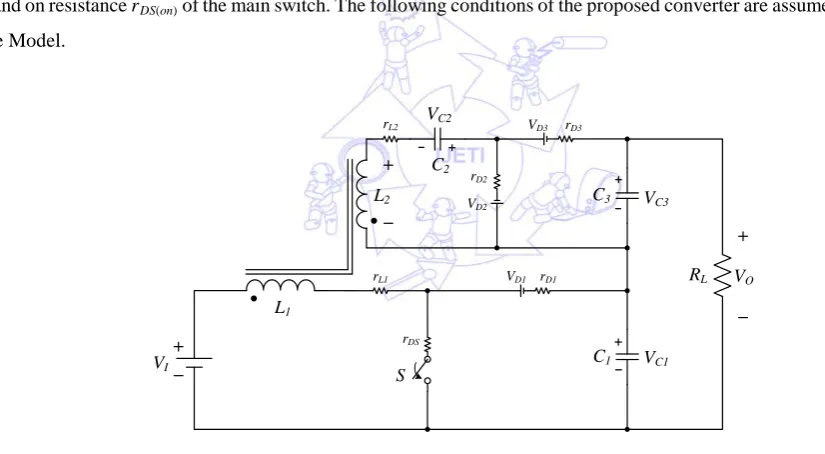
2.4. Effects of the ESRs of the Semiconductor Devices
Fig. 9 shows the equivalent circuit including inductor copper inductances rL1 and rL2, on resistances of diode rD1, rD2 and
rD3, and on resistance rDS(on)
VO
VI C1
C3
L1
L2
RL
VC1 VC3 C2
VC2
rDS
S
rD2
VD2
rD3 VD3
rD1 VD1 rL1
rL2
of the main switch. The following conditions of the proposed converter are assumed in this analysis
of the Model.
Fig. 9 Equivalent circuit with copper and semiconductor losses
(1) The main switch parasitic capacitor and the diode capacitor are excluded.
(2) During the switch is turned on can be modeled a resistance rDS(on)
(3) The diodes are modeled by the forward voltage V
, and during the switch turned off can be modeled an
infinite resistance.
D1, VD2 and VD3, and the forward resistances rD1, rD2 and rD3
(4) The effects of leakage inductances L
. When the
diodes are reversed-biased, they can be modeled by an infinite resistance.
k1and Lk2
(6) Assumed the magnetizing inductor is sufficiently large to ensure a small-ripple current approximation.
(7) To consider DC components during the off period, the average current is iL1 =iL1(t), and the average current is iL2 =iL2
(8) The capacitors C
(t).
1, C2 and C3 are assumed to be large enough and output voltage Vo
Based on the Kirchhoff’s voltage law (KVL) principle, during the switch S is turned on as shown in Fig. 10(a), the
following equations can be represented as follow
is constant.
1( ) 1 1
i L on L L DS DS
V =V + ⋅i r +i ⋅r (11)
(
)
1( ) 1 1
L on i L L DS
V
= −
V
i
r
+
r
(12)(
)
2
2 1( ) 2 2 2 2
1
C L on D L D D
N
V V i r r V
N
= − + − (13)
The current of capacitors C1, C2 and C3
1( )
o
C on o
L
V
i
i
R
= −
= −
are given as follows:
(14)
2( ) 2
C on D
i =i (15)
3( )
O
C on O
L V
i i
R
= − = − (16)
During the main switch S is turned off as shown in Fig. 10(b), the following equations can be represented as follow
(
)
1 + 1( ) 1 1+ 1 1
C i L off L L D D
V =V V −i r r −V (17)
(
)
2
C3 2 2 2 3 3
1
i C L L D D
N
V V V i r r V
N
= + − + − (18)
(
)
(
)
2
1 3 1( ) 2 1 1 1 2 2 3 1 3
1
1
o C C i L off C L L D L L D D D
N
V V V V V V i r r i r r V V
N
= + = + + + − + − + − −
(19)
The current of C1, C2 and C3
1( ) 1
o C off L
L
V
i i
R
= −
are givens as follow
(20)
2( ) 2
C off L
i
= −
i
(21)3( ) 2
o C off L
L
V
i i
R
= − (22)
(
)
(
)
(
)
(
)
(
)
(
)
1( ) 1 1 2 2 2
1 1 1 2 2 3
1 2 3
1
[ 1
1
]
L off O i L L DS D L D
L L D L L D
D D D
V V V n n i r r i r r
n
i r r i r r
V V V
= ⋅ − + + ⋅ + + +
+
+ + + +
+ + +
(23)
Based on the amp-second balance principle, from (14), (15), (16) and (20), (21), (22) can be rewritten as follows:
1( ) 1( )
0 0
S S
S
DT T
C on DT C off
i dt+ i dt=
∫
∫
(24)2( ) 2( )
0 0
S S
S
DT T
C on DT C off
i dt+ i dt=
∫
∫
(25)3( ) 3( )
0 0
S S
S
DT T
C on DT C off
i dt+ i dt=
∫
∫
(26)According to (26), the current flow path the C3
(
)
2 1 0
O O
S L S
L L
V V
DT i D T
R R
− ⋅ + − ⋅ − =
can be presented as
(27)
Form equation (27), the current iL2
2 1 1 O L L V i D R = ⋅ −
is determined as
(28)
According to (24), the current flow path on the C1
(
)
1 1 1 0 1 OS C S
L V
DT i D T
D R
− ⋅ ⋅ + ⋅ − =
−
can be presented as
(29)
Form equation (29), the current iL1
1 1 1 O L L V i D R = ⋅ −
is determined as
(30)
Substituting (28) into (25), the current flow path iD2
2 2 1 D L D i i D = −
can be derived as follows
(31)
(a) Switch turned on (b) Switch turned off
Where in the steady state, the principle of volt-second balance can be given as equation:
[
]
(
)
(
)
(
)
(
)
(
) (
) (
)
1 1 1 1
2 2 2 1 1 1
2 2 3 1 2 3
1
( ) 1 2
1
1
i L L DS S O i L L DS
D L D L L D
L L D D D D S
V i r r DT V V n n i r r
n
i r r i r r
i r r V V V D T
− + ⋅ = ⋅ − + + ⋅ +
+
+ + + +
+ + + + + ⋅ −
(32)
Where 2
1 N n
N =
From equation (34), the equation can be rewritten as
(
)
(
)
(
)
(
)
(
) (
)
}
1 1 1 1
2 2 2 1 1 1
2 2 3 1 2 3
1 1
1 1
O i L L DS L L DS
D L D L L D
L L D D D D
n n
V V i D r r i n r r
D D
i r r i r r
i r r V V V
+ + = − ⋅ + + ⋅ + − − + + + + + + + + + (33)
Substituting (28), (30) and (31) into (33), the equation can be rewritten as
(
)
(
)
(
)
(
)
(
) (
)
}
1 1 1 1 1 2 2
1 1 1 2 3 1 2 3
1 1
1 1 1
O i L L DS L L DS L L D
L L D L D D D D
n D
n D
V V i r r n i r r i r r
D D D
i r r r r V V V
+ + = − − − ⋅ + + ⋅ + + − ⋅ + + + + + + + + (34)
From equation (34), the voltage conversion ratio VO /Vi
(
)
(
)
(
)
(
)
1 2 3
1 1 1 1 2 1 3
2 1 1 1 1 1 1
1 1 1
1
(1 ) (1 )
D D D
i
O
i L L DS D L DS L D D
L L
V V V
n
n
D V
V D
V r n r r n r r n n r r r r
D R D R + + + ⋅ − ⋅ − + − = + + + + + + + ⋅ + + + + + − ⋅ − ⋅
is represented as follows
(35)
Where 2
1
N n
N
=
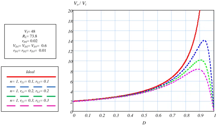
The voltage gain and efficiency affected by different ESRs with coupled inductor is shown in Fig. 11 and Fig. 12. The
maximal voltage gain is constrained by the equivalent series resistances, and the efficiency will be decreased by the extreme
duty ratio.
Vo / Vi
0 0.1 0.2 0.3 0.4 0.5 0.6 0.7 0.8 0.9 1
0 2 4 6 8 10 12 14 16 18 20 D VI= 48
RL= 73.8 rDS= 0.02 VD1= VD2= VD3= 0.6 rD1= rD2= rD3= 0.01
Ideal
n= 1, rL1= 0.1, rL2= 0.1
n= 1, rL1= 0.2, rL2= 0.2
n= 1, rL1= 0.3, rL2= 0.3
Efficiency(%)
0 0.1 0.2 0.3 0.4 0.5 0.6 0.7 0.8 0.9 1
0 10 20 30 40 50 60 70 80 90 100 110
D
VI= 48
RL= 73.8
rDS= 0.02
VD1= VD2= VD3= 0.6
rD1= rD2= rD3= 0.01
Ideal
n= 1, rL1= 0.1, rL2= 0.1
n= 1, rL1= 0.2, rL2= 0.2
n= 1, rL1= 0.3, rL2= 0.3
Fig. 12 Efficiency versus duty ratios under different ESRs with coupled inductor
Neglecting the equivalent series resistance of the proposed converter, the ideal voltage gain can be expressed as
2 1
1
1 O CCM
i
N
V N
M
V D
+
= =
−
(36)
According to (55), the equation can be reorganized and the equivalent circuit is shown in Fig. 13 as follows
(
1)
(
1)
1 1(
1)
(
1)
2(
1)
(
1)
i O L L DS L DX DX
V +n =V −D +i r +n +r +n +r +r −D +V −D (37)
Where 1 2 3
1
DX D D D
D
r r r r
D
= + +
−
1 2 3
DX D D D
V =V +V +V
iL1
iL1
iL1
iL1
(
1−D V)
O(
)
21−D RL
(
1)
i
V +n
(
)
1 1
L
r +n rL2 rDS
(
1+n)
rDX(
1−D)
DX V
Fig. 13 Equivalent circuit corresponding to Eq. 37
The input power and output power of the converter can be calculated as shown in equation (38) and (39), respectively.
2 1 1
1
in i L
N
P V i
N
= + ⋅
(38)
(
1)
1out O L
out
in P
P
η= (40)
According to the equation (38), (39) and (40), the converter efficiency can be derived as follows
(
)
(
)
(
)
(
)
1 2 3
1 1 1 1 2 1 3
2
1 1
1
1 1 1
1
(1 ) (1 )
D D D
i
L L DS D L DS L D D
L L
V V V
n
D V
r n r r n r r n n r r r r
D R
D R
η
+ +
+
− ⋅ −
=
+ + + + + + + ⋅ + + +
+ +
− ⋅
− ⋅
(41)
Where 2
1
N n
N
=
Efficiency (%)
VI= 48 RL= 73.8 rDS= 0.02 VD1= VD2= VD3= 0.6 rD1= rD2= rD3= 0.01
Ideal
n= 1, rL1= 0.1, rL2= 0.1 n= 5, rL1= 0.1, rL2= 0.5 n= 10,rL1= 0.1, rL2= 1
0 0.1 0.2 0.3 0.4 0.5 0.6 0.7 0.8 0.9 1
0 10 20 30 40 50 60 70 80 90 100 110
D
Fig. 14 The efficiency versus duty ratio under various turn ratios and ESRs
From equation (41) shows that the efficiency is affected by the equivalent series resistance. Fig. 14 shows the efficiency
affected by various turns ratios and ESRs.
2.5.
Gain
Duty
0 0.1 0.2 0.3 0.4 0.5 0.6 0.7 0.8 0.9 1
0 5 10 15 20 25 30 35 40 45 50
Proposed Converter Boost_Flyback Flyback Boost
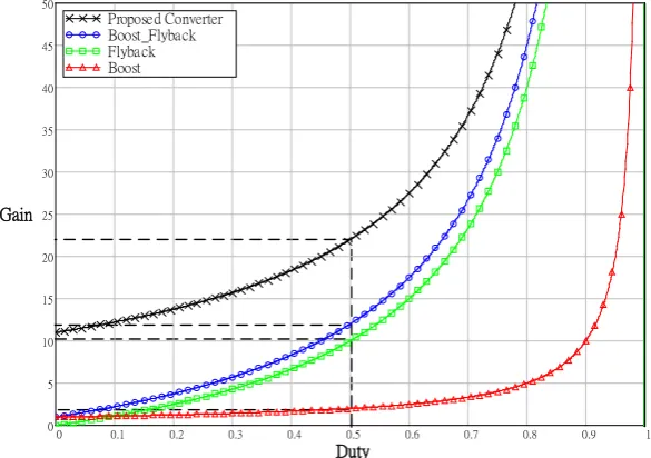
Comparison of Converter Voltage Gain
Fig. 15 shows a comparison of the converter voltage gain and the set N2 / N1 = 10. When working in a 50 % duty cycle, the boost converter voltage gain is the lowest.Second, the setting of the winding ratio is N2 / N1 = 10; therefore, the flyback converter voltage gain is greater than the boost converter.Theboost-flyback converter is a combination of the boost converter
and flyback converter. The structure has many advantages; however, the voltage gain is only slightly larger than that of the
flyback converter. The proposed step-up converter is improved with the boost-flyback converter, which has features and
benefits of the boost-flyback converter. Furthermore,
3.
the proposed converter has a much higher efficiency in voltage gain than
the other converters.
3.1.
Simulation and Experimental Results of the Proposed Converter
Simulation for The Proposed Converter
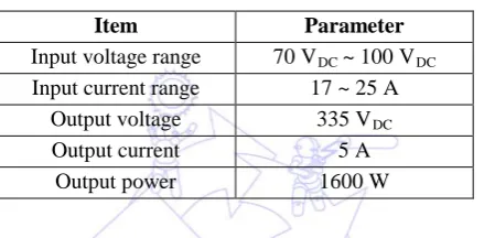
Software of SIMPLIS was used to simulate the proposed step-up converter in this study. The parameters of the circuit
design are shown in Table 1.
Table 1 Design parameters o
Item
f prototype
Parameter
Input voltage range 70 VDC ~ 100 VDC
Input current range 17 ~ 25 A Output voltage 335 VDC
Output current 5 A
Output power 1600 W
Fig. 16(a) shows the simulation waveform of 400W, which is able to tell that ILm lowest current has been greater than zero.
This means that the work patterns have full access to the continuous conduction mode. In addition, the circuit VDS voltage waveform is perfect in that and no spike is generated. The 1600W simulation waveform is shown in Fig. 16(b). The waveform
has not changed much since the operation at 400W into the continuous conduction mode afterward. Only the current peaks
gradually increased.
3.2. Experimental Results for The Proposed Converter
Table 2 Utilized components of prototype
Each component of the circuit is used in design that will affect efficiency. The experimental circuit parameters are shown
in Table 2.
Item Parameter
MOSFET S FQA65N20
Diode D1 V60200PG
Diode D2/ D3 20CTH03FP Magnetize inductance (Lm) 115uH
0.93uH Leakage inductance
N1:N2 38 : 55
PWM Control IC UC3845
33k Hz Operating frequency
ch1:VGS(10V/Div), ch2:VDS(100V/Div), ch3:Ii (10A/Div) ch1:VGS (10V/Div), ch2: VDS (100V/Div), ch3: Ii (20A/Div)
Fig. 17 Waveform measurement of proposed topology: (a) 400W, (b)
1600W
ch1:VGS(20V/Div), ch2:VI(100V/Div),ch3:VO(100V/Div), ch4:IO(5A/Div)
The waveform measurement of the proposed STEP-up Converter is shown in Fig. 17.The circuit can be measured by the waveform diagram similarly to the simulation results. The input and output voltage, and output current waveform are shown in
Fig. 18.
Fig. 19 Comparison of simulation and implementation efficiency
For experimental waveform measurement, the input supply voltage source involved seven 12V lead-acid batteries. The
output was a resistive load box,and the circuit efficiency of the simulation and experiment are shown in Fig. 19, which
demonstrated the highest efficiency of 97.09 % at 300W.Moreover, when at full load, 1600W demonstrated 93.81 % efficiency
performance. In addition, Fig.13 illustrates the efficiency that gradually decreased operate at 500W after. The main reason is
that when the power device conduction. The flow through power devices and the transformer input current resulting loss has
increased significantly (PLoss=I2R), which is a feature of the high power and high step-up converter. The d
4.
uty cycle can be raised
to resolve this problem of decreasing efficiency, and the current peaks can be smooth in a cycle. This is a feature of the past
involving the duty cycle being too high and resulting in decreased efficiency. After the increased duty cycle, the resulting loss
that parasitic elements is much smaller than the input current in the power components [14].
Conclusion
These voltages are low for photovoltaic systems, fuel cells, wind generators and uninterruptible power systems, whose
voltages are not high; therefore, they require high-gain and high-power converters to raise voltage supply devices such as power
grids and electric vehicles. Many high-power converters currently have control of complex and costly problems. The proposed
circuit topology improving high-gain ratio,increasing efficiency, reducing the secondary side of copper loss, and having an
active-clamp effect that can reduce the switch stress on power components and have the energy feedback mechanism. Such a
method of high efficiency and simple control can reduce cost and product size. The circuit configuration of the proposed
converter topology demonstrated the highest efficiency of 97.09 % at 300W in the experiment.M
References
oreover, when at full load,
1600W demonstrated 93.81 % efficiency performance.
[2]K. C. Tseng and T. J. Liang,
[3]Rong-Jong Wai and Rou-Yong Duan, “High step-up converter with coupled- inductor,” IEEE Transactions on Power Electronics, vol. 20, no.5, pp.
“Analysis of integrated boost-flyback step-up converter,” IEE Proc.-Electr. Power Appl., vol. 152, no. 2, pp. 217–225, April 2005.
[4]Rong-Jong Wai and Rou-Yong Duan, “High Step-Up Coupled-Inductor-Based Converter Using Bi-Direction Energy Transmission,” Power Electronics Specialists Conference, PESC '05. IEEE 36th, June 2005, pp.
1025–1035, 2005.
[5]Rong-Jong Wai , Chung-You Lin , Rou-Yong Duan , Yung-Ruei Chang , “High-efficiency DC-DC converter with high voltage gain and reduced switch stress,” IEEE Transactions on Industrial Electronics, vol. 54, no. 1, pp. 354–364, 2007.
406–412.
[6]Rong-Jong Wai, Chung-You Lin, Rou-Yong Duan and Yung-Ruei Chang, “High-Efficiency Power Conversion System for Kilowatt-Level Stand- Alone Generation Unit with Low Input Voltage,” IEEE Transactions on Industrial Electronics, vol. 55, no. 10, pp. 3702–3714, 2008.
[7]G. Spiazz, P. Mattavelli and A. Costabesssber, “Effect of Parasitic Components in the Integrated Boost-Flyback High Step-Up Converter,” Industrial Electronics, 2009. IECON '09. 35th Annual Conference of IEEE, pp.
[8]
420–425.
[9]
Shih-Kuen Changchien, Tsorng-Juu Liang, Jiann-Fuh Chen and Lung-Sheng Yang, “Novel high step-up DC–DC converter for fuel cell energy conversion system,” IEEE Transactions on Industrial Electronics, vol. 57, no. 6, pp. 2007–2017, 2010. Dwari, S.; Parsa, L., “An efficient high step-up interleaved DC-DC converter with a common active-clamp,” IEEE Transactions on Power Electronics, vol. 26, no. 1, pp. 66
[10]
–78, 2011.
Wuhua Li; Yi Zhao, Yan Deng and Xiangning He, “Performance analysis of an interleaved high step-up converter with voltage multiplier cell,” Applied Power Electronics Conference and Exposition (APEC), Twenty-Fifth Annual IEEE, Feb. 2010, pp.
[11]
1069–1074.
T. Dumrongkittigule, V. Tarateeraseth, and W. Khan-ngern, “A new integrated inductor with balanced switching technique for common mode EMI reduction in high step-up DC-DC converter,” EMC-Zurich 17th International Zurich Symposium on Electromagnetic Compatibility, Feb. 2006, pp.
[12]
541–544.
Ching-Tsai Pan and Ching-Ming Lai, “A high-efficiency high step-up converter with low switch voltage stress for fuel-cell system applications,” IEEE Transactions on Industrial Electronics, vol. 57, no. 6, pp. 1998–2006,
[13]
2010. K. B. Park, G. W. Moon and M.J. Youn,
[14]
“Non-isolated high step-up boost converter integrated with sepic converter,” IEEE Transactions on Power Electronics, vol. PP, no. 99, pp .1–1, 2010.