Copyright © 2015 CTTS.IN, All right reserved
VLSI Implementation of Neural Network
Jitesh R. Shinde1
Research Scholar & IEEE member, Nagpur, India Email:[email protected]
Suresh Salankar2
Professor, G.H.Raisoni College of Engineering, Nagpur, Maharashtra, India
Abstract — This paper proposes a novel approach for an optimal multi-objective optimization for VLSI implementation of Artificial Neural Network (ANN) which is area-power-speed efficient and has high degree of accuracy and dynamic range.
A VLSI implementation of feed forward neural network in floating point arithmetic IEEE-754 single precision 32 bit format is presented that makes the use of digital weights and digital multiplier based on bit serial architecture.
Simulation results with 45 nm & 90 nm tech file on Synopsis Design Vision Tool, Aldec’s Active HDL tool, Altera’s Quartus tool & MATLAB showed that the bit serial architecture (TYPE III) based multiplier implementation and use of floating point arithmetic (IEEE -754 Single Precision format) in ANN realization may provide a good multi-objective solution for VLSI implementation of ANN.
Keyword — Artificial Neural Network (ANN), bit serial architecture (type III) based multiplier, array multiplier, floating point arithmetic, multi-layered artificial neural network (MNN), Neural Network (NN), multi-layer perceptron (MLP).
1. I
NTRODUCTIONMulti-objective optimization can be defined as a technique which involves minimizing or maximizing multiple objective functions subjects to a set of constraints.
In conventional approach for VLSI implementation of digital circuits, there is always a tradeoff between area, power and speed i.e. optimizing the circuit for speed increases the area overhead in design and vice versa [1,2]. Optimizing one parameter affects the other as seen in equation below:-
*
L dd
d
C V
T
I (1.1) So, the objective of this research work is come to up with a step by step an optimal multi-objective approach for VLSI implementation of artificial feed neural network (NN) wherein all constraints viz. area, speed and power can be optimized simultaneously as well as the design should have high degree of precision and should provide dynamic weight reconfigurability.
2.
A
RTIFICIALN
EURALN
ETWORKANN is an information-processing system wherein neurons process information [3].
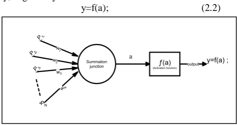
An artificial neuron forms the basic unit of artificial neural networks. The basic elements of an artificial neurons are (1) a set of input nodes, indexed by, say, 1, 2, ... N, that receives the corresponding input signal or pattern vector, say x=( P1, P2, ... , PN)T ; (2) a set of synaptic connections whose strengths are represented by a set of weights, here denoted by w=(w1,w2,...wI)T ; and (3) an activation function ‗a‘ that relates the total synaptic input to the output (activation) of the neuron. The main components of an artificial neuron are illustrated in Figure 2.1.
The total synaptic input, a, to the neuron is given by the inner product of the input and weight vectors:
N j j j=1
a=
W P ;
(2.1)where we assume that the threshold of the activation is incorporated in the weight vector. The output activation, y, is given by
y=f(a); (2.2)
Fig.2.1: Structural diagram of simple neuron
Copyright © 2015 CTTS.IN, All right reserved Fig.2.2: Block diagram representation of three-
layered MNN
3. D
ESIGNI
SSUES1. Data Representation: An important issue during hardware implementation of neural network is to strike a balance between the need for reasonable precision and cost associated with in logic overhead with increased precision [5]. So selection of proper arithmetic scheme viz. fixed point arithmetic scheme or floating point arithmetic is important.
- The fixed point arithmetic scheme will be
advantageous in application where degree of precision is not important and thus in such application it may provide a good multi-objective solution for optimizing cost of hardware and speed simultaneously. But fixed point arithmetic scheme does not provide a better option for dynamic weight re-configurability because as input changes, data bus size and hence the entire logic need to reconfigured every time as the number of bits used to represent weights are varied in order to enhance the precision and accuracy of system. Moreover, weights need to be processed first (i.e. truncated and rounded off) before applying to system and hence thereby increasing the simulation time.
- The floating point arithmetic scheme (IEEE 754-Single precision format (32 bit) or Double precision format (64 bit)) offers the greatest amount of dynamic range and eliminates the need of processing the weights ,and thereby making it good choice for neural network based applications where high degree of precision is desired. But the hardware implementation for floating point arithmetic is costlier and the speed of processing is low due to double calculations i.e., separate calculation for mantissa and exponent.
2. Analog versus Digital Neural network
- The computational density of chip is defined as amount of computation per unit silicon. The computational density of analog neural network is 10 to 100 times greater than that of digital neural network because complex non-linear operations such as multiply, divide and tangent can be implemented with handful of transistors in a analog network in
comparison to digital network which requires hundreds of transistor or even thousands of transistor to perform the same operation. Thus, precision of analog neural network is directly proportional to area of the chip.
- The speed of analog neural network is inversely proportional to area of chip. Smaller the area of chip less will be the time taken by signal to propagate to output or from one circuit component to other. Moreover, the parasitic capacitance will also be less and thereby further enhancing the speed of the circuit.
- The power consumption of analog circuit is directly proportional to the speed at which circuit operates. A large percentage of power consumed is dissipated as heat during normal operation of the circuit. For given speed and circuit architecture, efficiency of power dissipation decreases with the area of chip but this will be accompanied by degradation in the precision of circuit
- One common approach to reduce power requirement
of analog circuit is to reduce operating voltages. However the immediate effect will be reduce dynamic range of all signals in circuits and hence affecting the precision of circuit.
- Digital neural network are inherently robust for effects such as substrate noise, power supply variation, radiation, matching, noise, drift, mobility reduction and so on. In analog networks, these effects can be minimized but at the cost of increased power consumption and area of circuit.
- An analog network must be full custom design. Digital Designs are flexible since it allows software control and arbitrary level of precision (low to high, and fixed or floating point). They can be generated from logic description of its function.
- Loading of digital weights is easy in comparison to loading of analog weights since no feedback is required.
- Analog neural networks are harder to scale with new processes and require total redesign. Digital neural networks scale easily with new processes and require no redesign.
Above conclusions drawn from (6, 7, 8, 9) suggest that analog neural networks are suitable for classification problems where minimum power consumption is main design constraint i.e. single objective optimization goal and digital neural networks may be suitable for classification problems where design constraints are precision, area, power and speed i.e. multi-objective optimization.
3. Multiplier Unit
Copyright © 2015 CTTS.IN, All right reserved area, speed and power consumption of the circuit [1, 2,
10, and 11]. MCM (Multiple Constant Multiplication) approach may not be suitable in digital neural network because here requirement is that weight needs to be fixed. So, dynamic weight adjustment will not be possible because it may require redesigning entire block [1, 2].
4.
D
ESIGNA
PPROACH FOR OPTIMIZATIONTo realize multi-objective optimized i.e. high degree of
precision, area-speed-power optimized VLSI
implementation for ANN following approaches were selected:
- Floating point arithmetic scheme (IEEE 754-single precision (32 bit) format to have high degree of precision.
- Digital neural network may enable in realizing the multi-objective optimization goal.
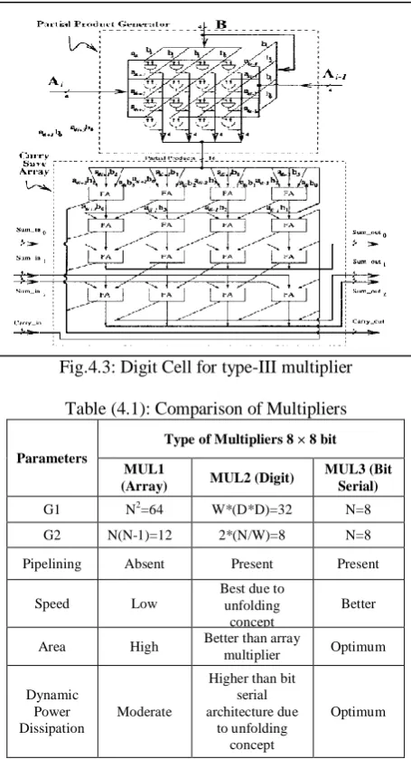
- Array multiplier or multiplier unit based on bit serial architecture or digit serial architecture (Type 3) (14, 15). Block schematic of multiplier unit based on bit serial architecture and digit serial architecture are shown in figure 4.1, 4.2& 4.3 respectively.
Fig.4.1: An example of 4×4 Array multiplier
Bit - serial arithmetic and communication is efficient for computational processes, allowing good communication within and between VLSI chips and tightly pipelined arithmetic structures. It is ideal for neural networks as it minimizes the interconnect requirement by eliminating multi - wire busses [16].
Comparative analysis of multiplier (N*N) with respect to multiplicand data size ‗A‖ & multiplier data size of N=8 in both cases are shown in table 4.1.
Fig.4.2: Bit-serial type-III multiplier with word-length of 4 bits
Fig.4.3: Digit Cell for type-III multiplier
Table (4.1): Comparison of Multipliers
Parameters
Type of Multipliers 8 × 8 bit
MUL1
(Array) MUL2 (Digit)
MUL3 (Bit Serial)
G1 N2=64 W*(D*D)=32 N=8
G2 N(N-1)=12 2*(N/W)=8 N=8
Pipelining Absent Present Present
Speed Low
Best due to unfolding
concept
Better
Area High Better than array
multiplier Optimum
Dynamic Power Dissipation
Moderate
Higher than bit serial architecture due
to unfolding concept
Optimum
Where description of notations G1, G2 used in above table is as follows:
- G1 => approximate number of AND gates required for partial product implementation.
- G2 => approximate number of Full Adders required. - Digit size D=N/W=4. No. of folding W=2.
Comparative analysis suggests that bit serial architecture (Type III) provides better trade off to realize
multi-objective optimization approach for VLSI
Implementation of digital neural network.
i. Criteria for FPGA selection & high performance:
- Any FPGA is suited to bit serial design. The first consideration is whether there are sufficient logic elements and I/O resources to support the design. Most bit serial designs have a very low routing complexity, so the routing resources are not an issue. - The entire design should be synchronous, including
Copyright © 2015 CTTS.IN, All right reserved - Use hierarchy in the design.
- Add pipeline registers to break up long delays.
-V.
D
ESIGN&
I
MPLEMENTATIONIn our work, we had designed and implemented VLSI digital ANN viz. ANN using array multiplier approach (fnn1test1) & ANN using multiplier approach based on bit serial architecture (Type III) (bsfnn1_test1).
The experimental setup flow used in this research work is as follows:
Step I: IMPLEMENTATION IN MATLAB: The data that used in this project was acquired from University of California, Irvine (UCI Machine Learning Repository). The first objective of this study was to determine whether an Iris flower is of versicolour, virginica or setosa. And also to identify the fit training settings for building classification model for Iris. The attributes information is given in Table 5.1.
Table 3.1: Description of attributes
After observing data set it was observed that only two attributes viz. petal length and petal width were sufficient to classify whether an Iris flower is of versicolour, virginica or setosa. Thus, by reducing dimension of input data set we were able to optimize the simulation runtime considerably in MATLAB.
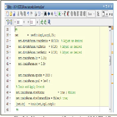
To ensure a correct comparison of different types of neural networks, the division of input data into training, validation and test sets is performed by independent part of code and the division result is stored. The partitioning of input data is performed randomly with a certain ratio of input entities to be stored as training set, validation set and test set. The experimental settings for this done in MATLAB to classify data using neural toolbox is shown in figure 4.1 and 4.2 respectively and result i.e. trained graphs obtained showing 100 % fit is shown in figure 5.1, 5.2 and 5.3 respectively.
Fig.5.1: Neural net specification in of MATLAB
Trained graph of iris data indicates type of iris. The plot describes the attribute and classes with target and distribution the iris data. Basically the training purpose is to identify the fit training settings for model.
Fig.5.2: Neural network specification in nn traintool of MATLAB
No Physical
Attribute
Features
1. sepal length Used as Input
2. sepal width Used as Input
3. Petal length Used as Input
4. Petal width Used as Input
5. Target Used as Output:
Copyright © 2015 CTTS.IN, All right reserved Fig.5.3: Trained graph showing 100% fit
STEP II : IMPLEMENTATION in VHDL: The weights of stage 1(fw11, fw22) and stage 2 (fw33) (refer fig 3.2) obtained from this trained graph were first converted into IEEE 754 single precession 32 bit binary format in MATLAB and were used in stage 1 and stage 2 of VLSI implementation of neural network shown in figure (5.4).
ANN in this research work uses three layer feed forward neural network architecture which has two input neuron, fifteen hidden neuron and one output neuron. Inputs to the ANN are a 32 bit number in IEEE-754 single precision format, represent attributes petal length and petal width of iris flower and output is 32 bit number in IEEE-754 single precision format, represent a prediction to which category flower belongs.
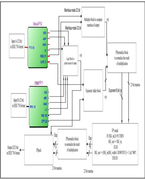
The flow the input data in generalized block schematic structure of IEEE 754 single precision multiplier block used is shown in figure (5.5).
Fig.5.4: RTL view of VLSI Implementation of neural network
Fig.5.5: Generalized block schematic structure of IEEE 754 single precision multiplier block
Unpack block unpacks incoming data (31 down to 0) into three parts viz. sign bit (MSB 31st bit), exponent (30 down to 23) and mantissa (22 down to 0). This blocks maps 23 bit mantissa into 32 bit by appending zeros at LSBs.
Packfp block packs final result of multiplication obtained after normalization & rounding i.e. its mantissa, exponent and sign bit into IEEE -754 single precision formats. Unpackfp and packfp block also checks the exponent and mantissa part of inputs for the following conditions (underflow (de-normalized number), overflow, infinity and not a number (NaN) to find the 32 bit input data and hence output (via FPpack block & logic block to predict nature of output) is a valid IEEE 754 single precision floating point number [12, 13].
Table 5.1: Table listing conditions to check nature of input
Number sign exponent mantissa
normalized number 0/1 01 to FE any value De-normalized
number (underflow) 0/1 00
any value
zero 0/1 00 0
infinity (Overflow) 0/1 FF 0 NaN i.e Not a Number
(inf*0 or inf/inf or 0/0 form)
FF any value but not 0
0 50 100 150
Copyright © 2015 CTTS.IN, All right reserved The IEEE 754 standard partially solves the problem of
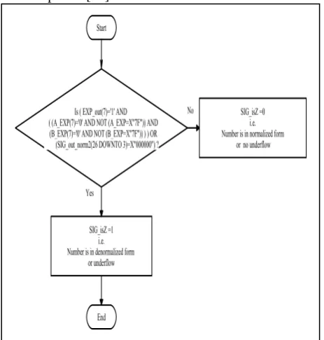
underflow by using de-normalized representations in which a de-normalized representation is characterized by an exponent code being all 0's, interpreted as having the whole part of the significand being an implied 0 instead of an implied 1[12].
Fig.5.6: Flowchart representing logic used in program to check for underflow condition
Multiplier block performs the multiplication of two input data (mantissa) coming from unpackFP0 & unpackFP1 block and generates mantissa part of final output. Output data bus of multiplier blocks implementated with array multiplier logic 32bit×32bit (figure 4.1) was of 64 bit and total partial product inferred were 64. Output data bus of multiplier block implemented with bit serial logic (figure 4.2) was 24 bit and number of AND gates inferred to implement partial product were 24.
Exponent adder blocks add exponent parts of respective exponent parts of input A and B to generate exponent of output Z.
The RTL view of ANN using array multiplier and ANN using bit serial architecture (Type III) based multipliers are shown in figure 5.7 & 5.8 respectively.
FPnormalize block checks whether 23 bit mantissa‘s MSB bit is one or zero. If it is one then mantissa is in normalized form and FPnormalize block converts de-normalized mantissa into de-normalized form.
The FPround block performs the function of rounding.
Fig.5.7: RTL view of ANN using array multiplier
Fig.5.8: RTL view of ANN using bit serial architecture (Type III) based multiplier
Floating-point numbers are coded as "sign/magnitude", reversing the sign-bit inverses the sign. Consequently the same operator performs as well addition or subtraction according to the two operand's signs.
Floating-point addition progresses in 4 steps:
- Mantissa alignment if A and B exponents are different,
- Addition/subtraction of the aligned mantissas, - Renormalization of the mantissas sum S if not
already normalized - Rounding of sum S'.
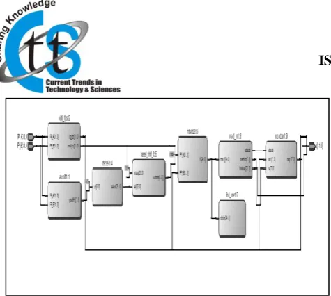
The floating point adder block diagram used is shown in figure 5.9. The major entities in this block diagram are bigfp_fps, absdiff1 blockdecsel1 block, barrel_shift_R block, intadd23 block, readadj_mj block and expadder1 block respectively. Each block description is as follows:- 1. bigfp_fps block :- The function of this block is to
Copyright © 2015 CTTS.IN, All right reserved Fig 5.9: RTL view of floating point adder
- Let given numbers are A=0101 and B=1000 where first bit i.e. A (3) & B (3) represents sign bit of given number.
- bigtemp <= FP_A when (not(FP_A(3))&FP_A(2 downto 0)) > (not(FP_B(3))&FP_B(3 downto 0)) else FP_B;
- smalltemp <= FP_A when
(not(FP_A(3))&FP_A(2 downto 0)) <
(not(FP_B(3))&FP_B(2 downto 0)) else FP_B; - big_op <= smalltemp when (FP_A(3)
and FP_B(3)) > '0' else bigtemp ;
- small_op <= bigtemp when (FP_A(3) and FP_B(3)) > '0' else smalltemp ;
- The result of program will be big_op <=A & small_op <=B.
Fig 5.10: Flow graph for logic used in bigfp_fps block
2. absdiff1 block :- This block find the larger of the two exponent and outputs the absolute value of the exponent difference as shown in figure 5.11.
Fig 5.11: Flow graph for logic used in absdiff1 block
3. decsel1 block: - This block outputs the information by how many bit smaller mantissa should be shifted be shifted depending on input coming from output of absdiff1 block. The "implicit bit" is added, totaling 24 bits.
4. barrel_shift_R block:- This block shifts the smaller operand mantissa (small_op (23 down to 0)) towards right by number coming from output of decsel1 block.
5. intadd23 block:- This block computes the addition of two floating point numbers (24 bit) using 2s-complement arithmetic and result obtained is of 25 bits.(figure 5.11). Here, if addsub= ‗0‘, the two numbers are added, else the subtraction is performed using 2s-complement arithmetic.
Fig 5.11: Flow graph for logic used in intadd23 block
6. readj_m1 block :- This block checks 25 bit result i.e. mantissa of intadd23 block and performs following three tasks viz. :
Copyright © 2015 CTTS.IN, All right reserved onethloc = ―00000001‖ or man1(0)= ‗1‘, then
onethloc = ―00010111‖ else onethloc = ―00011000‖. - It readjusts the mantissa block.
- It outputs addsub =0 if man1(24 and 23 )= '0' else addsub = ‗1‘.
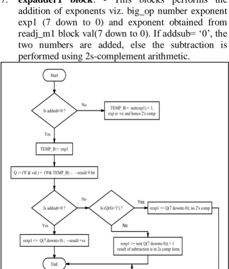
7. expadder1 block: - This blocks performs the addition of exponents viz. big_op number exponent exp1 (7 down to 0) and exponent obtained from readj_m1 block val(7 down to 0). If addsub= ‗0‘, the two numbers are added, else the subtraction is performed using 2s-complement arithmetic.
Fig 5.12: Flow graph for logic used in expadder1 block
VI.
R
ESULTS&
C
OMPARISONThe code for of ANN using array multiplier and ANN using bit serial architecture (Type III) based multiplier were written in Aldec Active HDL tool and synthesized on Altera‘s Quartus tool and it was targeted on FPGA Cyclone 2, Device EP2C70F672C6. Later on code was also tested at Backend on Synopsis tool on 45 nm & 90 nm tech file. FPGA implementation of ANN array multiplier & using bit serial architecture (Type III) based multiplier were clearly classifying iris data into 3 categories: - output corresponding to counter‘s count value from 1 to 50 represented iris setosa, output corresponding to counter‘s count value from 51 to 96 represented iris versicolour and output corresponding to counter‘s count value from 97 to 143 represented iris virginica. This was found to be matching with iris flower data set.
The performance comparison of implemented ANN at frontend and backend VLSI design are given in table 6.1 and 6.2 respectively and graphical representation of total cell area and total dynamic power dissipation are shown in figure 6.1 and 6.2 respectively.
The experimental results at Backend VLSI design level indicates that ANN using bit serial architecture Type III
based multiplier is better than ANN using array multiplier in
- Total Cell area saving in 90 nm & in 45 nm: - 62.681 % & 60.65 % respectively.
- Total area saving in 90 nm & in 45 nm: - 63.86 % & 60.65 % respectively.
- Total dynamic power saving in 90 nm & in 45 nm: - 53.81 % & 90.88 % respectively.
Table 6.1: Performance comparison of implemented neural networks at frontend level
Parameters 32×32 bit
NN using
Array Multiplier
NN using Bit serial architecture based (Type III) Multiplier Total Logic
Elements 63038 62725
Embedded
multipliers 300/300 0/300
Total dynamic power
dissipation(mW)
40.14 6
Data arrival time
tco(nsec) 300.023 273.496
Table 6.2: Performance comparison of implemented neural networks at backend level
Parameters 90 nm tech file 45 nm tech file (no
Workload model)
Array Bit Arra
y
Bit Total Area
nm2
2333944 843437 -- --
Total cell area nm2
2193638 818627 897092 353045
Total dynamic power dissipation
5.1803 mW
2.393 mW 148.468 mW
13.554 mW
Data arrival time nsec
90.9 1.5 141.5 1.14
The performance comparison of implemented multiplier at backend VLSI design is given in table 6.3 and 6.4 respectively.
Table 6.3: Performance comparison of implemented multipliers 32 × 32 bit at backend level
Parameters 90 nm tech file 45 nm tech file (no Workload model)
Array Bit Array Bit
Total area nm2
20677.4997 57
5420.97173 6
-- --
Total cell area (nm2)
20007.0145 59
5304.72962 6
19676.34075 9
2185.06077 1 Total
dynamic power dissipation( mW)
0.5913478 0.0275544 6.3856 0.0312965
Data arrival time (nsec)
19.89 4.19 1.93 1.34
Copyright © 2015 CTTS.IN, All right reserved
Parameters of multiplier 32×32 bit
Array Multiplier
Bit Serial architecture based multiplier (Type III)
Total Logic Elements 234 209
Total dynamic power dissipation(mW)
6.11 0.54
Worst propagation delay
41.604 21.495
VII.
C
ONCLUSIONSThe realization of bit serial architecture Type III based multiplier implementated in floating point arithmetic provides a good trade off in realizing high end applications which is area-speed-power efficient with good precision and dynamic range. The bit serial architecture Type III based multiplier approach suggested in this paper were found to be giving better performance than other promising findings available in literature [17, 18, 19, 20, 21, 22, 23, 24, 25] . Hence, the realization of ANN design using bit serial architecture Type III based multiplier implementated in floating point arithmetic (IEEE 754- single precision format) has presented a new approach for multi-objective optimization of VLSI implementation of neural network. It has also proven to be better alternative over ANN design using array multiplier.
Future research work system by improvising adder unit block if possible and a full characterization of each design option at layout level.
R
EFERENCE[1] Jitesh Shinde, S. Salankar, ―Multi-objective
Optimization for VLSI Circuits‖, IEEE
International Conference on Computational Intelligence & Communication Networks‖, November 14-16, 2014, Kolkata, India
[2] Jitesh Shinde, S. Salankar, ―Optimal Multi-objective Approach for VLSI Implementation of Digital FIR Filters‖, International Journal of Engineering Research & Technology (IJERT), Vol. 3, pg. no. 2470-74, Issue 2, February – 2014. [3] S N Sivanandam, S Sumathhi, S N DEEPA, ―
Introduction to Neural Networks Using MATLAB 6.0‖, ch no 1,2 , pg no.1 to 26, (Tata McGraw-Hill, 2006).
[4] Amos R. Omondi, Jagath C. Rajapakse, ― FPGA
Implementation of Neural Networks‖, ch no 1, pg no 3 to 6, (Springer, 2006).
[5] Suhap Sahin, Yasar Becerikli, and Suleman Yazici, ―Neural Networks Implementation in Hardware using FPGAs‖, ICONIP 2006, Part III, LNCS 4234, pp.1105, 2006, © Springer-Verlag Berlin Heidelberg 2006.
[6] Sorin Draghici, ―Neural Networks in Analog Hardware – Design and Implementation Issues,‖ International Journal of Neural Systems, vol. 10, no. 1 (February, 2000), 19-42, © World Scientific Publishing Company.
[7] Dan Hammerstorm, ―Digital VLSI for Neural Networks‖, Department of Electrical and Computer Engineering, OGI School of Science & Engineering, Portland, Oregon.
[8] Vipan Kakkar, ―Comparative Study on Analog and Digital Neural Networks‖, International Journal of Computer Science and Network Security, vol.9, no.7, July 2009.
[9] Nelson Morgan, Krste Asanovic, Brian Kingsbury, John Wawrzynek, ―Developments in Digital VLSI Design for Artificial Neural Networks‖, TR-90-065.
[10] Biederman D.C., Ososanya, ―Design of a neural network-based digital multiplier‖, System Theory,
1997., Proceedings of the Twenty-Ninth
Southeastern Symposium, Cookeville, TN, page no. 320 – 326, 9-11 Mar 1997.
[11] Uroˇ s Lotricˇ, Patricio Bulic, ―Applicability of approximate multipliers in hardware neural networks‖, Neurocomputing Elsevier (2012), SciVerse ScienceDirect.
[12] Jean-Michel Muller, Nicolas Brisebarre, Florent de Dinechin, Claude-Pierre, Jeannerod Vincent Lef`ever, Guillaume Melquiond, Nathalie Revol, Damien Stehl´ e, Serge Torres, ― Handbook of floating point arithmetic‖, Birkh¨auser Boston, part of Springer Science+Business Media.
[13] A.Nagoor Kani, ―Digital Signal Processing‖, ch.8, Tata McGrawhill.
[14] Yun-Nan Chang,Student Member, IEEE,
Janardhan H. Satyanarayana, Member, IEEE, and Keshab K. Parhi, Fellow, IEEE, ―Systematic Design of High-Speed and Low-Power Digit-Serial Multipliers‖, IEEE Transactions on Circuits and Systems—II: Analog & Digital Signal Processing, Vol. 45, no. 12, December 1998. [15] Ms.P.J.Tayade, Dr. Prof. A.A.Gurjar, ―Systematic
Design of High-Speed and Low-Power Digit-Serial Multipliers VLSI Based‖, International Journal of Management, IT and Engineering, Vol. 2, Issue 5, Pg. no. 439-446, May 2012.
[16] Alan F. Murray, Anthony V. W. Smith and Zoe F. Butler, ―BIT -SERIAL NEURAL NETWORKS‖, American Institute of Physics 1988.
[17] Kumar Mishra, V.Nandanwar, Eskinder Anteneh Ayele, S.B.Dhok, ― FPGA Implementation of Single Precision Floating Point Multiplier Using High Speed Compressors‖, International Journal of Soft Computing & Engineering, Vol. IV, Issue II, May 2014.
[18] B.Jeevan, S.Narendra, Dr. C.V.Reddy, Dr.
K.Sivani, ―A High Speed Binary Floating Point Multiplier Using Dadda Algorithm‖, IEEE 2013. [19] Shaifali, Sakshi, ― FPGA Design of Pipelined
Copyright © 2015 CTTS.IN, All right reserved [20] Chaitali V. Matey, Dr. S.D. Chede, S.M.Sakhare, ―
Design & Implementation of Floating Point Multiplier Using Wallace and Dadda Algorithm‖, International Journal of Application or Innovation in Engineering & Management‖, Vol. III, Issue VI, June, 2014.
[21] Summit Vaidya, Deepak Dandekar, ―Delay-Power
Performance Comparison of Multipliers in VLSI Circuit Design‖, International Journal of Computer Networks & Communications (IJCNC)‖, Vol. II, Issue IV, July 2010.
[22] M.K.Pavuluri, T.S.R. Krishna Prasad,
Ch.Rambabu ―Design & Implementation of Complex Floating Point Processor using FPGA‖, International Journal of VLSI Design & Communication Systems (VLSICS)‖, Vol. IV, Issue V, October 2013.
[23] Prashant Kumar Sahu, Nitin Meena, ―Comparative Study of Different Multiplier Architectures‖, International Journal of Engineering Trends & Technology (IJETT)‖, Vol. IV, Issue X, October 2013.
[24] Deepak Purohit, Himanshu Joshi, ― Comparative Study & Analysis of Fast Multipliers‖, International Journal of Engineering & Technical Research (IJETR), Vol. II, Issue VII, July 2014.
[25] Anitha R, Alekhya Nelapati, L.Jesima W,
V.Bagyaveereswaran, ― Comparative Study of High Performance Bruan‘s Multiplier using FPGAs‖, IOSR Journal of Electronics & Communication Engineering (IOSRJECE)‖, Vol. I, Issue IV, pp 33-37, May-June,2012.
A
UTHOR’
SP
ROFILEJitesh R. Shinde received B.E. Degree in
Electronics & Telecommunication
Engineering from and M. Tech Degree in VLSI from Rashtrasant Tukadoji Maharaj Nagpur University in 2005 & 2007 repectively. He has also done C-DAC diploma in VLSI Design in 2008. He has also done specialization in IC Layout Engineering certified by University of California, Santacruz Extension and Cadence from TIIT, Hyderabad in 2008. He is doing research in VLSI domain from Rastrasant Tukadoji Maharaj Nagpur University, Nagpur. His current research focuses on VLSI design, Digital Signal Processing, Neural Network.
Suresh S. Salankar, received B. E. Degree in Power Electronics from
Bapurao Deshmukh College of
Engineering, Sevagram in 1987, M.Tech in System and Control Engineering from Indian Institute of Technology, Bombay in 1994, Ph.D in Electronics and Telecommunication Engineering from Swami Ramanand Teerth Marathwada University, Nanded, India in 2008. He is currently