Design, Implementation and Performance Analysis of
4-bit Full Ripple Carry Adder Using Adibatic Logic in
45nm CMOS Sub-micron Technology
Jitendra R. Patel, Prof. Sandip Nemade, Prof. Vikas Gupta
Abstract—In this paper I had implemented the different three types of 4-bit adder using adiabatic logic and conventional CMOS logic in 45nm technology with LT spice. As we know Full adders are important components in applications such as digital signal processors (DSP) architectures and microprocessors. Apart from the basic addition adders also used in performing useful operations such as subtraction, multiplication, division, address calculation, etc. we have compared all three techniques conventional CMOS, 1n-1p Quasi and 1n-1p split level logic in 1-bit as well as 4-bit adder for power dissipation and as result suggest adiabatic method has low power dissipation compared to conventional CMOS. We got minimum power dissipation and energy consumption in 1n-1p split adiabatic logic.
Keywords—Adibatic Logic, DSP, CMOS, Low Power.
I. I
NTRODUCTIONPower consumption and it’s minimization is one of the
primary concerns in today VLSI design methodologies because of two main reasons one is the long battery operating life requirement of mobile and portable devices and second is due to increasing number of transistors on a single chip leads to high power dissipation and it can lead to reliability and IC packaging problems.
Adiabatic logic reduces the energy dissipation by reducing the dissipation across resistances of conducting MOSFETs and recovering the part of energy given to the output back to the source, which extends the battery life. Several adiabatic logic styles are available but here we implemented two styles are 1n-1p Quasi adiabatic logic and 1n-1n Split level adiabatic logic. As we know Full adders are important components in applications such as digital signal processors (DSP) architectures and microprocessors. Apart from the basic addition adders also used in performing useful operations such as subtraction, multiplication, division, address calculation, etc.
II. A
DIABATIC ANDC
ONVENTIONALC
HARGINGA. Conventional charging
The dominant factor of power dissipation in a conventional CMOS device is the dynamic power required to charge and discharge the capacitive nodes within the
Is withdrawn from supply. Only half of this energy is temporarily stored in capacitor CL. The remaining
= 0.5 . (2)
Is dissipated as heat in the on resistance of PMOS. When input becomes logic high, the NMOS turns on and energy stored on capacitor CL is discharged to the ground and dissipated as heat. Hence during a complete charge-discharge cycle, the energy
= . (3)
Is withdrawn from power supply and is dissipated as heat. Half of this energy is dissipated during charging and half is dissipated during discharging.
B. Adiabatic Charging
When you submit your final version, after your paper has been accepted, prepare it in two-column format, including figures and tables.
In static CMOS logic, the abrupt application of supply voltage gives rise to high potential across the switching device. The energy dissipation during charging and discharging can be minimized to a great effect by ensuring that the potential across switching device is kept sufficiently small. Adiabatic charging may be achieved by charging the capacitor from a time varying source that starts at 0V. This time varying source rises towards V at a slow rate that ensures that potential across switching device is kept arbitrarily small. The adiabatic charging is shown in figure 1.
Fig.1. Adiabatic charging
In fact the energy dissipated across the resistance, R is
.= . = . . (4)
From the above equation (4), we can see that if T >> RC, the energy dissipation during charging Ediss ≈ 0.
Copyright © 2013 IJECCE, All right reserved Where, Vs is the voltage swing.
III. D
ESIGN ANDI
MPLEMENTATION OFA
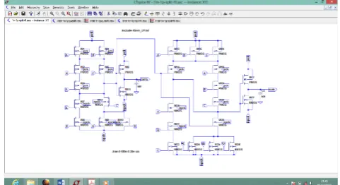
DDERSDifferent adiabatic logic styles contain different number of transistors and different number of power clocks. In this section we will study different adiabatic logic styles, which are derived from static CMOS, without large change: 1n1p split-level pulse adiabatic logic, 1n1p quasi adiabatic logic and conventional CMOS style from which both adiabatic style are derived.
A.
1n-1p Quasi full adder
The 1n1p quasi adiabatic logic basically, it is similar to conventional CMOS except, it includes a sinusoidal power clock instead of dc power supply. By implementing 1n1p quasi adiabatic logic, it is possible to achieve quasi adiabatic operations with conventional static CMOS gates under one phase driving. If driver is varied sufficiently slowly, dissipation occurs only during charging and discharging of load capacitor [7]. The sources of power dissipation in 1N1P quasi adiabatic logic are threshold voltage of MOSFET and energy dissipated in NMOS and PMOS resistance while charging and discharging of load capacitance. The use of slowly varying power clocks ensures the small energy dissipation across the ON resistance of MOS devices.
Fig.2. Schematic of 1-bit 1n-1p quasi full adder
Fig.3. Simulation result of 1-bit 1n-1p quasi full adder
Fig. 4 Schematic of 4-bit 1n-1p quasi ripple carry full adder
Figure 2, and figure 3 shows schematic of 1-bit full adder and it’s simulation result, while figure 4, and figure
5 shows 4-bit ripple carry adder and it’s simulation result.
Fig.5. Simulation result of 4-bit 1n-1p quasi ripple carry full adder
B.
1n-1p Split level adder
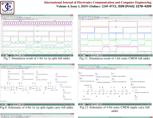
The second adiabatic logic family that we are going to discuss is 1n1p split-level pulse adiabatic logic. It comprises a conventional CMOS gate with two complimentary split-level pulse voltages. The peak voltage of each clock supplies is VDD/2 to the gates. In this logic family, the dissipation occurs solely from a finite rate of change of driving voltage and can be decreased to any desired level figure 6, and figure7 shows the schematic and its simulation result for 1 bit full adder, while figure 8, and figure 9 shows 4-bit ripple carry full adder.
Fig.7. Simulation result of 1-bit 1n-1p split full adder
Fig.8. Schematic of 4-bit 1n-1p split ripple carry full adder
Fig.9. Simulation result of 4-bit 1n-1p split ripple carry full adder
C.
Conventional adder
The conventional full adder design using static CMOS design the schematics to realize the Carry and Sum functions of a full adder are shown in figure 10, figure 11
shows it’s simulation result, while figure 12, figure 13
shows 4-bit ripple carry adder and simulation result of it.
Fig.11. Simulation result of 1-bit static CMOS full adder
Fig.12. Schematic of 4-bit static CMOS ripple carry full adder
Fig.13. Simulation result of 4-bit static CMOS ripple carry full adder
IV. C
OMPARATIVEA
NALYSIS OFA
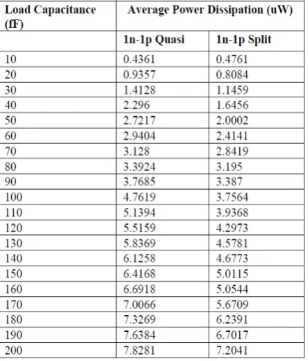
DDERSCopyright © 2013 IJECCE, All right reserved Table 1: Power Dissipation of 1-bit Full Adder
Table 2 : Power Dissipation of 4-bit Adiabatic Full Adder
Fig.14. Graphical representation of 1-bit adder power dissipation
V. C
ONCLUSIONFrom all results display by graph and observed from the table 1 and table 2, we comes to know the adiabatic family has a low power dissipation compared to static CMOS adder, while in adiabatic technology 1n-1p Quasi has the high power dissipation as shown in graphical representation the power dissipation is linearly increases with increase in load capacitance, whereas in 1n-1p split level somewhat lower power dissipation
Fig.15. Graphical representation of 4-bit Adibatic adder power dissipation
A
CKNOWLEDGMENTI want to sincerely say thanks to my guide Proff. Sandip Nemae to guide and choose such a level of work for me, at last but not least I thank full to all staff of department who help me directly or indirectly.
R
EFERENCES[1] Praveen Saxena, dinesh Chandra and Sampath kumar, Design Of “A 1-Bit Full Adder For Low Power Application”, in (IJAEST) International Journal Of Advanced Engineering Sciences And Technologies Vol No. 10, Issue No. 1, 019–025, 2011.
0 5 10 15
10 30 50 70 90 110 130 150 170 190
Po
w
er
Di
ss
ip
at
io
n
(u
W
)
Load Capacitance (fF)
1-bit Adder Comparative
Analysis
static CMOS 1n-1p Quasi
1n-1p Split
0 2 4 6 8 10
10 30 50 70 90 110 130 150 170 190
Po
w
er
Di
ss
ip
at
io
n
(u
W
)
Load Capacitance (fF)
4-bit Adibatic Adder Comparative
Analysis
[2] Y. Sunil Gavaskar Reddy and V.V.G.S.Rajendra Prasad, “The Power Comparison Of Cmos And Adiabatic Full Adder Circuits” in International Journal of VLSI design & Communication Systems (VLSICS) Vol.2, No.3, September 2011.
[3] Praveen Saxena, dinesh Chandra and Sampath kumar, “An Adiabatic Approach For Low Power Full Adder Design”, in International Journal on Computer Science and Engineering (IJCSE) Vol. 3 No. 9 september 2011.
[4] Subodh Wairya, Rajendra Kumar Nagaria and Sudarshan Tiwari, “Comparative Performance Analysis of XOR/XNOR Function Based High-Speed CMOS Full Adder Circuits For Low Voltage
VLSI Design,” in International Journal of VLSI design & Communication Systems (VLSICS) Vol.3, No.2, April 2012. [5] A. Kishore Kumar, D. Somasundareswari, V. Duraisamy, T.
Shunbaga Pradeepa, “Design of Low Power Full Adder using Asynchronous Adiabatic Logic” in European Journal of Scientific Research ISSN 1450-216X Vol.63 No.3 (2011), pp. 358-367.
[6] The Manoj Kumar, Sandeep K. Arya and Sujata Pandey,“Single bit full adder design using 8 transistors with novel 3 transistors XNOR gate” in International Journal of VLSI design & Communication Systems (VLSICS) Vol.2, No.4, December 2011.
[7] R.UMA, Vidya Vijayan, M. Mohanapriya, Sharon Paul,“Area, Delay and Power Comparison of Adder Topologies” in International Journal of VLSI design & Communication Systems (VLSICS) Vol.3, No.1, February 2012.
[8] Jin-Fa Lin, Yin-Tsung Hwang, Ming-Hwa Sheu, and Cheng-Che Ho, “A Novel High-Speed and Energy Efficient 10-Transistor
Full Adder Design”IEEE Trans. Circuits and Systems, vol. 54, No. 5, pp. 1050–1059, May 2007.
[9] Dai Jing. Hu Jianping, Zhang Weiqiang, Wang Ling,“Adiabatic CPL circuits for sequential logic systems”, IEEE MWSCAS’06, pp.713-717, August 2006.
[10] Ilham Hassoune and Denis Flandre,“ULPFA: A New Efficient
Design of a Power-Aware Full Adder”IEEE Trans. Circuits and Systems, vol. 57, No. 8, pp. 2066–2074, August 2010.
[11] Jianping Hu; Weiqiang Zhang; Xien Ye; Yinshui Xia; “Low
power adiabatic logic circuits with feedback structure using three-phase power supply”, in Proceedings of International Conference on Communications, Circuits and Systems, Vol. 2, 27-30, May 2005.
[12] A. P. Chandrakasan, S. Sheng and R. W. Bordersen, (1992) “Low-power CMOS digital design,”IEEE Journal of Solid-State Circuits, Vol. 27, No. 4, pp. 473- 484.
[13] Abdulkarim Al-Sheraidah, Yingtao Jiang, Yuke Wang and Edwin Sha, (2001)“A Novel Low Power Multiplexer-Based Full
Adder,” European Conference on Circuit Theory and Design, Espoo, Finland, pp. I329-I332.
[14] Uming Ko, Poras T. Balsara and Wai Lee, (1995)“Low-Power Design Techniques for High- Performance CMOS adders,” IEEE Transactions on Very Large Scale Integration (VLSI) Systems, Vol. 3, No. 2, pp. 327-333.
[15] Subodh Wairya , Garima Singh, Vishant, R. K. Nagaria and S. Tiwari (2011), “Design Analysis of XOR (4T) based Low Voltage CMOS Full Adder Cell,” In Proceeding of IEEE International Conference on Current Trends In Technology (NUiCONE’11), Ahmedabad, India pp. 1-7.