Implementation of Fuzzy Logic Controller
forStep-Up Converter Combining KY and
Buck-Boost Converter with Soft-Switching
Technic
Arya .P.R1, Saritha Sathyan2
PG Student [PE], Dept. of EEE, Sree Narayana Gurukulam College of Engineering, Kadayiruppu, Kerala, India1
Associate Professor, Dept. of EEE, Sree Narayana Gurukulam College of Engineering, Kadayiruppu, Kerala, India2
ABSTRACT: In this paper, a novel voltage gain enhanced step-up converter is presented. This converter is the combination of KY and synchronous BUCK-BOOST converter. Here the voltage gain enhancement is done by using coupled inductor with turns ratio and one charging pump. The output current of the converter is nonpulsating, hence the voltage stress across the output capacitor is less. Soft –switching technic is implemented for reducing the switching losses. Switch on time ZVS and switch off time ZCS will happen. In this project, a closed loop DC-DC KY and BUCK-BOOST converter circuit was designed and simulated using MATLAB SIMULINK based on a topological circuit. In this simulation, the circuit was tested with PI controller &FUZZY controller. PI controller and Fuzzy Logic Controllers are designed and implemented in the circuit with calculated duty cycle of the MOSFET. The outcome has indicated better performance for KY and BUCK-BOOST step-up converter with FLC controller.
KEYWORDS: KY converter, Synchronous BUCK-BOOST converter, Coupled inductor, Charging pump, High Voltage Gain,Soft-switching, Fuzzy Logic Controller.
I. INTRODUCTION
Renewable energy sources have experienced a rapid development in recent years. These systems employ with micro sources like PV, fuel cells etc. PV cells to produce high voltage but there exist severe problems like shadowing effects, short circuit which significantly reduces its efficiency. In order to overcome such unfavourable conditions this type of micro source energy is applied to the high step up converter to produce high voltage and fulfil the demands. In rapid progress of communication and computing gadgets DC-DC converters are employed for various devices like amplifiers, personal digital assistant (PDA), MP3 players, blue tooth devices etc., which need high voltage to obtain enough output power and voltage amplitude.
This converter is the combination of one KY and one Buck-Boost converter. Here the voltage gain can be enhanced by synchronous buck-boost converter and coupled inductor. A synchronous buck-boost converter is similar to buck boost converter with the diode is replaced by a MOSFET switch. The main objective is to improve the voltage gain of the step-up converter and also to reduce switching loss.Switching losses can be reduced by adding resonance converter.Further the voltage drift problem is reduced using closed loop control of the proposed converter with fuzzy logic controller.
II. LITERATURE SURVEY
components. Hence the circuit will become complex and also the final output stage suffers a high voltage stress. Luo converter is the one of the voltage boosting converter [4], but it needs two or more inductors and also possesses the drawback of right half plane zero
The KY buck-boost converter is a recently introduced step-up converter .This converter produces a high voltage gain. Step-up convertor is a combination of one charging pump and a coupled inductor with turns ratio [5]. This voltage gain can be achieved either by adjusting the duty cycle or by turns ratio ie, the duty cycle and the turns ratio are independent. This converter always works in CCM, Keeping the output current non-pulsating, hence voltage stress across the output capacitor will be suppressed but the switching loss is high. Switching loss can be reduced by adding resonance circuit which is a good solution for switching loss.
A novel soft switching isproposed and applied to the KY converter. Such a soft switching needs only one additional small inductor and oneadditional small capacitor, and this occupies only small spacein the circuit of the KY converter.[6]
A fuzzy logic controller for the conventional DC-DC converters has been reported in [7]. The FLC for all the converters has produced lesser output voltage start-up overshoots and lower output voltage ripple as compared to PI controller.
III. CIRCUIT DESCRIPTION
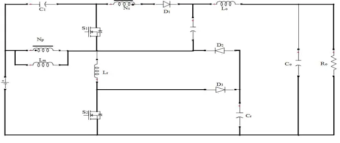
Fig 1 shows the KY and Buck-BOOST converter with soft switching technic. Prior to taking up this section, for the convenience of analysis, this converter contains two MOSFET switches namely and along with their body diodes and . A coupled inductor with primary turns and secondary turns which is used to obtain high voltage gain. Capacitor is energy transferring capacitor and capacitor is charge pump capacitor. Three diodes , . At the output side, one output inductor , one output capacitor is connected. The load is signified as . The input voltage and output voltages are represented as and respectively. A resonance inductor and a resonance capacitor which is used for soft switching purpose .So the voltages across switches are zero during turn off period and current trough the switches are zero during the turn on period. Besides, since the energy-transferring capacitor , operating based on the charge pump principle, are quickly charged to some voltages within a very short time.
Fig 1: Soft-Switched KY and Buck-Boost Converter
IV. PRINCIPLE OF OPERATION
Coupling coefficient k is equal to one, i.e., the leakage inductor is absent. The following analysis contains the description of the power flow path for each mode, along with the corresponding equations and voltage gain. Essentially, there are five operating modes in the proposed converter. Moreover, the gate driving signals and
indicated by , the current through is denoted by , the current through is denoted by . On the other hand, the voltage across or the voltage across the winding is represented by , the voltage across the winding is signified by , the voltage across is represented by , the voltage across is represented by , the voltage across is denoted by and the voltage across is denoted by .
MODE I
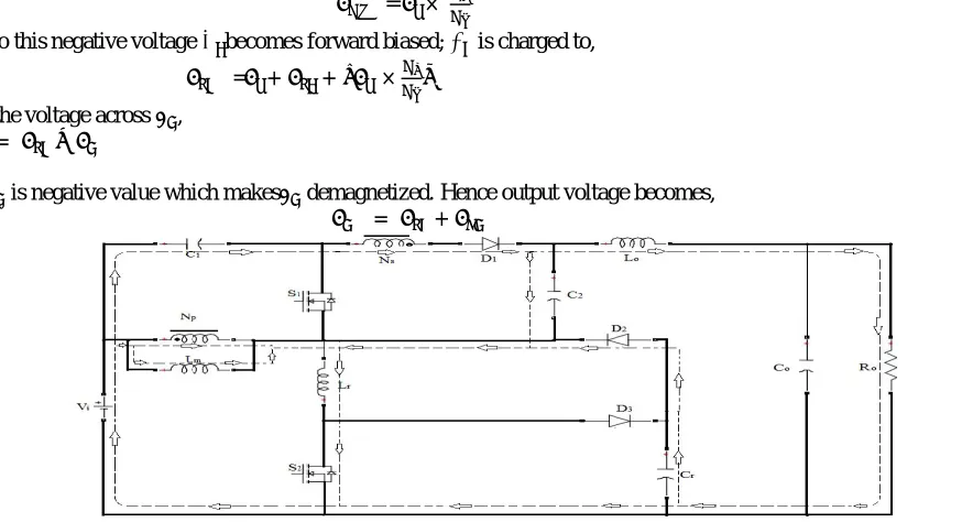
In this mode switch is turned on and switch is turned off. Two power flow path is there, one is energy provided to load and another is charging the resonance capacitor through resonance inductor. Thus the voltage across capacitor Cr increases slowly which is responsible for zero voltage turn off switch . First, − voltage is imposed on . Due to this negative voltage, will be demagnetized.
The voltage induced across the secondary winding equal to,
= − × ……….. . (1)
Due to this negative voltage induced in the secondary winding, diode becomes reverse-biased. Voltage across the load inductor becomes,
= + + − ……… (2) The voltage induced across the load inductor is positive value, thus causing to be magnetized. And provides energy to the load ,
= + + + ……… (3)
Fig 2: Mode I Operation ofthe Converter
MODE II
Switch is still on and switch is off. When the voltage across resonance capacitor increases and it exceeds the voltage across the energy transferring capacitor , the direction of current becomes reverse. The switch conducts through the anti-parallel diode. This is shown in figure 3
MODE III
When the resonance capacitor charged to its extreme value, that voltage is hold on . Direction of power flow shown in the fig 4
Fig 4: Mode III Operation ofthe Converter
MODE IV
Mode IV is shown in fig 4.5. In this mode of operation, the input voltage is imposed on , thus causing magnetizing inductor to be magnetized. The switch is turned off and switch S2 is turned on. Due to the presence of , the current through switch increases slowly which is responsible for zero current turn on of switch . The energy stored in the resonance capacitor is discharged slowly through diode and resonance inductor , This voltage comes across switch . Thus zero voltage turned off will occur.
The voltage induced across the secondary winding equal to,
= × ………. (4)
Due to this negative voltage becomes forward biased; is charged to,
= + + × ……… (5)
And the voltage across ,
= − ………. (6)
ie, is negative value which makes demagnetized. Hence output voltage becomes,
= + ……… (7)
MODE V
In this mode, switch is still on and switch is off. The capacitor Cr completely dischargesand the power flow is shown in fig 6.
Fig 6: Mode V Operation ofthe Converter
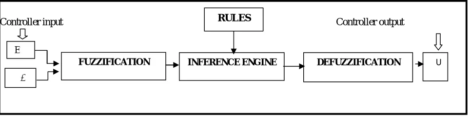
V. FUZZY LOGIC CONTROLLER
Fuzzy logic system is an intelligent system which is easy to understand, simple to design and better than using the other type of controller.In Fuzzy logic controller, better tuning of fuzzy will provide better output. This logic allows modelling of complex systems by combining alternative way of thinking using a higher level of abstraction. The variables of fuzzy logic are described for the control algorithm which influences the system variables and a rule table. The gain is defined as a division between the input voltage and average output voltage value.
Controller input Controller output
Fig7: Block diagram of FLC
The block diagram of fuzzy logic controller (FLC) is shown in fig.7. It consists of three main blocks: fuzzification, inference engine and defuzzification. The two FLC input variables are the error E and change in error ∆E. Depending on membership functions and the rules FLC operates. Mamdani type fuzzy logic scheme is used here.
DEFUZZIFICATION INFERENCE ENGINE
FUZZIFICATION E
∆U
RULES
Fig 8:Membership function for error
There are three membership functions for the input variable error. Fig. 8 shows the membership functions of input variable error.
Fig 9: Membership function for deltaerror
There are three membership functions for the input variable deltaerror. Fig. 9 shows the membership functions of input variable deltaerror.
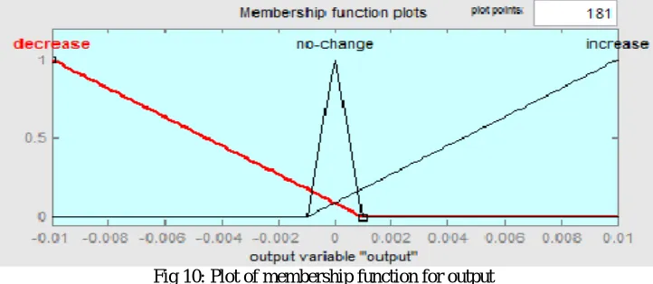
Fig 10: Plot of membership function for output
Fig 11: Surface View of Rules of FLC.
Fig.11 shows the representation of the typical Rule Surface of fuzzy logic controller. The Surface View of rules are represented as the combinations of the two inputs error and change in error for a function of output.
Five rules are used for obtaining fuzzy controlled output. They are:
1) If (error is negative ) then (output is decrease)
2) If (error is zero) and (output is negative) then (output is decrease) 3) If (error is zero) and (output is zero) then (output is no-change) 4) If (error is zero) and (output is positive) then (output is increases) 5) If (error is positive) then (output is increases)
VI. SIMULINK MODEL
To verify the practicability and validity of the KY and Buck-Boost converter. MATLAB/ Simulink software is applied for the simulation of the converter with both the controllers (PI and FUZZY). The proposed topology, as shown in Fig1. Input voltage = 12V, Output voltage =72V. Component values are selected is verified via MATLAB simulation, Coupled inductor n= ∶ = 1:3, =148.7 ,C1 = 470 , C2= 100 F, L0 = 188 µH = 470 ,
resonance inductor =10 and resonance capacitor = 10nf.
Fig 12:PI controller based on Simulink model
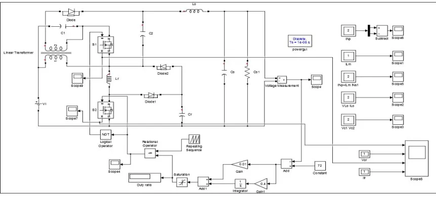
Fig13: Fuzzy controller based on Simulink model
Fig.13shows the simulink model of the proposed converter using FUZZY logic controller
VII. REUSLT AND DISCUSSION
Fig14: Input voltage 12V
12V DC is given to the input of the converter is shown in fig.14
0 0.01 0.02 0.03 0.04 0.05 0.06 0.07 0.08 0.09 0.1
11 11.2 11.4 11.6 11.8 12 12.2 12.4 12.6 12.8 13
Time (Seconds)
V
o
lt
a
g
e
(
V
o
lt
s
)
Fig 15:Output voltage waveform of the converter using FLC and PI Controller
The fig.15 shows the output voltage obtained from converter with FLC and PI. Output from FLC gives better performance when compared to converter with PIC. Output from the fuzzy controller will have reduction in settling time, reduction in output voltage overshoot and ripples, however output from PI will have a vice versa result.
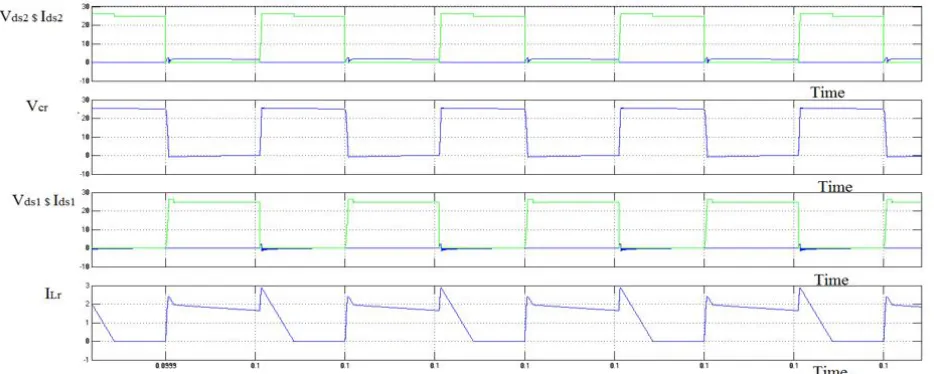
Fig 16 :(1) voltage and current across S1 (2)Voltage across VCr (3) Voltageand current across S2 (4) current flows
through ILr
Voltage and current across switch is represented as and respectively. Similarly voltage and current across switch in represented as and respectively. Zero current turn on and zero voltage turn off is obtained for both switches. Figure 16 (3) and (1) shows the voltage and current across switch and switch respectively. Fig 16(2) shows the voltage across VCr and fig.16(4) shows the current through the resonant inductor. Switch is turned
on first. The current across switch S1 increases slowly due to the presence of resonance inductor. This will lead to zero
current turn on in . Simultaneously, voltage across switch S2 increases gradually. i.e., the resonance capacitor is charging gradually and the voltage will come across switch S2. Hence the voltage is zero when is turned off which results in zero voltage switching when switch is turned on, the current will increase slowly due to the presence of a series inductor which leads to zero current turn on. During this period, zero voltage turn off will happen in switch .
0 0.01 0.02 0.03 0.04 0.05 0.06 0.07 0.08 0.09 0.1
VIII.CONCLUSION
Implement a fuzzy logic control for a step-up dc–dc converter by combining the coupled inductor and the switched capacitor with soft switching technic is simulated. A high step-up voltage gain is achieved. The corresponding voltage gain is higher than that of the existing step-up converter combining KY and buck-boost converters. As the output voltage of the converter is controlled with FLC has minimum overshoot, ripple and produces a constant output current which shows better performance when compared to the converter with PI controller. Additionally, the switch voltage stress is reduced by soft switching technic.Furthermore, the proposed converter has no floatingoutput, and it has one output inductor; hence, the outputcurrent is nonpulsating. Moreover, the structure of the proposedconverter is quite simple and very suitable for communication system and photo-voltaic applications.
REFERENCES
[1] Y. Deng, Q. Rong, Y. Zhao, J. Shi, and X. He, “Single switch high step-up converters with built-in transformer multiplier cell”, IEEE Trans. Power Electron., vol. 27, no. 8, pp. 3557–3567, Aug. 2012.
[2] W. Li,W. Li, X. He, D. Xu, and B.Wu, “General derivation law of nonisolated high-step-up interleaved converters with built-in transformer”,IEEETrans. Ind. Electron., vol. 59, no. 3, pp. 1650–1661, Mar. 2012.
[3] Y. Hsieh, J. Chen, T. Liang, and L. Yang, “Novel high step-up dc–dc converter for distributed generation system”, IEEE Trans. Ind. Electron., vol. 60, no. 4, pp. 1473–1482, Apr. 2013
[4] F. L. Luo, “Analysis of super-lift luo-converters with capacitor voltage drop”, in Proc. IEEE ICIEA, 2008, pp. 417–422.
[5] K. I. Hwu, Member, IEEE, and W. Z. Jiang, “Voltage Gain Enhancement for a Step-Up Converter Constructed by KY and Buck-Boost Converters”, IEEE Trans On Industrial Electronics, vol. 61, no. 4, April 2014