ISSN (Print) : 2320 – 3765 ISSN (Online): 2278 – 8875
I
nternational
J
ournal of
A
dvanced
R
esearch in
E
lectrical,
E
lectronics and
I
nstrumentation
E
ngineering
(An ISO 3297: 2007 Certified Organization)
Vol. 5, Issue 4, April 2016
Implementation of Low Power Arithmetic
Circuits Using Reversible Gates
N.Nagaraju1, C.Sushmitha2, R.Swathy3, S.Veenadevi4, S.A.Esther Jeba Rani5
Assistant Professor, Dept. of ECE, Adhiyamaan Engineering College, Hosur, Tamilnadu, India 1 UG Scholar, Dept. of ECE, Adhiyamaan Engineering College, Hosur, Tamilnadu, India 2,3
ABSTRACT : In current scenario, the reversible logic design attracting more interest due to its low power consumption and smaller area. The main purpose of designing reversible logic are to decrease quantum cost, depth of the circuits, and number of garbage outputs. Reversible logic have theoretically zero internal power dissipation because they do not lose information. Low power consumption and smaller area are important criteria for high performance systems. Reversible logic has the feature to generate one to one correspondence between its input and output. As a result no information is lost and there is no loss of energy. Thus the vector of input state can always be reconstructed from the vector of output states.
KEYWORDS : Low power, VLSI, Reversible logic, Reversible gates, Quantum cost, Garbage
I. INTRODUCTION
The design of arithmetic circuits using conventional gates consumes more power and area occupied by the design is also large, inorder to reduce the power consumed by the gates reversible logic is used. Reversible logic gates produce zero power dissipation under ideal conditions. Hence these are preferred for low power design applications such as quantum computing and Nano technology. The quantum cost of the reversible logic circuit can be minimized by reducing the number of reversible logic gates.
A. REVERSIBLE LOGIC
Everyone in the world of modern circuit design tries to reduce the power consumption by the circuit. As demonstrated by R.Landauer in the early 1960s, irreversible hardware computation, regardless of its realization technique, results in energy dissipation due to the information loss [1]. Also prove that Reversible logic circuits have theoretically zero internal power dissipation because they do not lose information. Hence, in 1973, Bennett showed that in order to avoid KTln2 joules of energy dissipation in a circuit, it must be built using reversible logic gates [2]. A circuit is said to be reversible if the input vector can be uniquely recovered from the output vector and there is a one-to-one correspondence between its input and output assignments, i.e. not only the outputs can be uniquely determined from the inputs, but also the inputs can be recovered from the outputs. This project presents design of low power reversible logic arithmetic circuits such as full adders and multipliers. The project is organized as follows chapter II presents the literature survey on reversible logic gates, chapter III presents the design of full adders, chapter IV presents the design of 4-bit ripple carry adder, chapter V presents the design of multipliers, chapter VI presents results and discussions, chapter VII presents conclusion and future enhancements.
B. MULTIPLIER
ISSN (Print) : 2320 – 3765 ISSN (Online): 2278 – 8875
I
nternational
J
ournal of
A
dvanced
R
esearch in
E
lectrical,
E
lectronics and
I
nstrumentation
E
ngineering
(An ISO 3297: 2007 Certified Organization)
Vol. 5, Issue 4, April 2016
Fig 1.1: 4*4 multiplier
C. SOFTWARE & HARDWARE DETAILS
Xilinx ISE is a software tool produced by Xilinx for synthesis and analysis of HDL designs, enabling the developer to synthesize ("compile") their designs, perform timing analysis, examine RTL diagrams, simulate a design's reaction to different stimuli, and configure the target device with the programmer. The Processes hierarchy describes the operations that the ISE will perform on the currently active module. The hierarchy includes compilation functions, their dependency functions, and other utilities. The window also denotes issues or errors that arise with each function. The Transcript window provides status of currently running operations, and informs engineers on design issues.
A Field Programmable Gate Array (FPGA) is an integrated circuit designed to be configured by a designer after manufacturing-hence Field Programmable. The Spartan-3 generation of FPGA is used for the implementation of these circuits.
II. LITERATURE SURVEY
A. FEYNMAN GATE
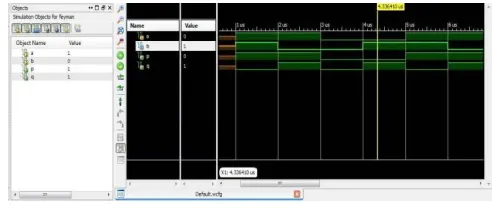
Richard P. Feynman [3][7] discusses the physical limitations associated with building computers of very small size. He introduces the concept of reversible logic gates. The Feynman gate which is a 2*2 gate and is also called as Controlled NOT and it is widely used for fan-out purposes. The inputs (A, B) and outputs P=A, Q= A XOR B. It has Quantum cost one.
Fig 2.1: Block diagram of Feynman gate The simulated output is shown above
B. TOFFOLI GATE
ISSN (Print) : 2320 – 3765 ISSN (Online): 2278 – 8875
I
nternational
J
ournal of
A
dvanced
R
esearch in
E
lectrical,
E
lectronics and
I
nstrumentation
E
ngineering
(An ISO 3297: 2007 Certified Organization)
Vol. 5, Issue 4, April 2016
Fig 2.3: Block diagram of Toffoli gate The simulated output is shown above
C. FREDKIN GATE
The Fredkin gate [4][7] (also CSWAP gate) is a computational circuit suitable for reversible computing, invented by Ed Fredkin. It is universal, which means that any logical or arithmetic operation can be constructed entirely of Fredkin gates. The Fredkin gate is the three-bit gate that swaps the last two bits if the first bit is 1.Fredkin gate which is a 3*3 gate with inputs (A, B, C) and outputs P=A, Q=A'B+AC, R=AB+A'C. It has Quantum cost five.
Fig 2.5: Block diagram of Fredkin gate The simulated output is shown above
D. PERES GATE
Peres Gate (PG) [7] is composed of two XOR gate and one AND gate as shown in Figure 2.7. Figure 2.7 shows a 3x3 Peres gate (Peres, A., 1985, Ali M., 2012). The input vector is I (A, B, C) and the output vector is O (P, Q and R). The output is defined by P = A, Q = A⊕B and R=AB⊕C. Quantum cost of a Peres gate is 4.
Fig 2.7: Block diagram of Peres gate The simulated output is shown above
E. DKG GATE
ISSN (Print) : 2320 – 3765 ISSN (Online): 2278 – 8875
I
nternational
J
ournal of
A
dvanced
R
esearch in
E
lectrical,
E
lectronics and
I
nstrumentation
E
ngineering
(An ISO 3297: 2007 Certified Organization)
Vol. 5, Issue 4, April 2016
Fig 2.9: Block diagram of DKG gate The simulated output is shown above
III.DESIGN OF FULL ADDER
A. FULL ADDER USING CONVENTIONAL GATES
Full adder [6] consists three inputs (A, B, Cin) and two outputs (sum, carry).It is designed using EX-OR, AND, OR gate. It is totally designed with six gates.
Figure3.1: Logic diagram of Full adder The simulated output is shown above
B. FULL ADDER USING PERES GATE
It consists of three inputs (A, B, ‘0’) and three outputs (P, Q, R).Implementation of full adder circuit using PERES gate is shown below:
Figure 3.2: Full adder using peres gate The simulated output is shown above
C. FULL ADDER USING DKG GATE :
ISSN (Print) : 2320 – 3765 ISSN (Online): 2278 – 8875
I
nternational
J
ournal of
A
dvanced
R
esearch in
E
lectrical,
E
lectronics and
I
nstrumentation
E
ngineering
(An ISO 3297: 2007 Certified Organization)
Vol. 5, Issue 4, April 2016
Figure 3.3: Full adder using DKG gate The simulated output is shown above
IV. DESIGN OF 4-BIT RIPPLE CARRY ADDER
A. DESIGN OF 4-BIT RIPPLE CARRY ADDER USING CONVENTIONAL GATES
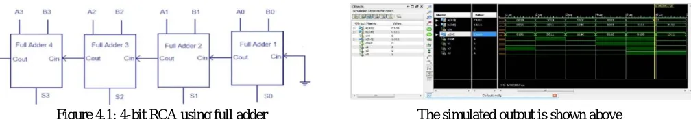
It consists of inputs [A (3 down to 0), B (3 down to 0)] and outputs [sum and carry]. Implementation of full adder circuit using conventional gate is shown below:
Figure 4.1: 4-bit RCA using full adder The simulated output is shown above
B. DESIGN OF 4-BIT RIPPLE CARRY ADDER USING DKG GATES
It consists of inputs [A (3 down to 0), B (3 down to 0), ‘0’, Cin] and outputs [sum and carry].Implementation of full adder circuit using DKG gate is shown below:
Figure 4.2: 4-bit RCA using DKG gate The simulated output is shown above
C. DESIGN OF 4-BIT RIPPLE CARRY ADDER USING PERES GATES
It consists of inputs [A (3 down to 0), B (3 down to 0), ‘0’, Cin] and outputs [2-garbage outputs for each gate, sum and carry]. Implementation of full adder circuit using PFAG gate is shown below:
ISSN (Print) : 2320 – 3765 ISSN (Online): 2278 – 8875
I
nternational
J
ournal of
A
dvanced
R
esearch in
E
lectrical,
E
lectronics and
I
nstrumentation
E
ngineering
(An ISO 3297: 2007 Certified Organization)
Vol. 5, Issue 4, April 2016
V. DESIGN OF MULTIPLIER
A. DESIGN OF 4*4 MULTIPLIER USING CONVENTIONAL GATES
4*4 multiplier is a circuit for the multiplication of two 4-bit inputs and the output is displayed as a 8-bit product.
Figure 5.1: 4*4 multiplier using full adder The simulated output is shown abov
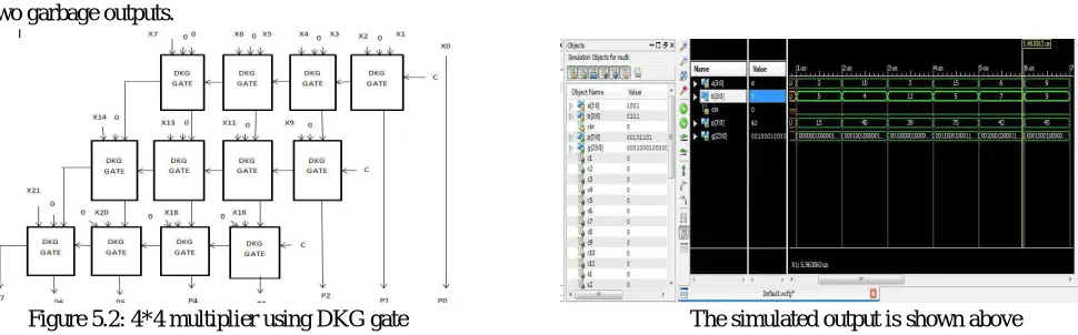
B. DESIGN OF 4*4 MULTIPLIER USING DKG GATES
It is a 4*4 multiplier designed using DKG gates which have 4 inputs and 4 outputs. Here, each gate produces two garbage outputs.
Figure 5.2: 4*4 multiplier using DKG gate The simulated output is shown above
C. DESIGN OF 4*4 MULTIPLIER USING PERES
4*4 multiplier is designed using peres gate having four inputs and four outputs, in which two garbage outputs are produced from each peres gate.
ISSN (Print) : 2320 – 3765 ISSN (Online): 2278 – 8875
I
nternational
J
ournal of
A
dvanced
R
esearch in
E
lectrical,
E
lectronics and
I
nstrumentation
E
ngineering
(An ISO 3297: 2007 Certified Organization)
Vol. 5, Issue 4, April 2016
D. DESIGN OF 8*8 MULTIPLIER
8*8 multiplier circuit is designed using conventional gates such as full adder circuit and AND gates.
Figure 5.4: 8*8 multiplier The simulated output is shown above
E. DESIGN OF 8*8 MULTIPLIER
Design of 8*8 Multiplier using DKG gate is done and the simulated output is shown below:
VI. RESULTS AND DISCUSSIONS
A. COMPARISON BETWEEN CONVENTIONAL AND REVERSIBLE GATES FOR 4-BIT RCA
4-Bit Ripple Carry Adder
Number of Gates used
Conventional gates 24
DKG gates 4
Peres gates 4
B. COMPARISON BETWEEN CONVENTIONAL AND REVERSIBLE GATES FOR 4*4 MULTIPLIER
4*4 Multiplier Number of Gates used
Conventional gates 88
DKG gates 28
ISSN (Print) : 2320 – 3765 ISSN (Online): 2278 – 8875
I
nternational
J
ournal of
A
dvanced
R
esearch in
E
lectrical,
E
lectronics and
I
nstrumentation
E
ngineering
(An ISO 3297: 2007 Certified Organization)
Vol. 5, Issue 4, April 2016
C. COMPARISON BETWEEN CONVENTIONAL AND REVERSIBLE GATES FOR FULL ADDER
D. COMPARISON BETWEEN CONVENTIONAL AND REVERSIBLE GATES FOR 8*8 MULTIPLIER
8*8 Multiplier Number of Gates used
Conventional gates 376
DKG gates 116
VII. CONCLUSION AND FUTURE ENHANCEMENTS
A. CONCLUSION
In our proposed design the number of gate, number of constant input are very less as compared to previous design. In our design we have low power and less area which is most important in designing area. In low power arithmetic circuits we have designed circuits using FREDKIN gate, PERES gate and FEYMAN gate, TOFOLLI gate and DKG GATE. We have compared these proposed designs with the existing designs in terms of number of gates used, Garbage outputs, constant inputs, logical & arithmetic functions, and hardware complexity. In future we can design complete computer architecture with the help of proposed designs.
B. FUTURE ENHANCEMENT
Results of the presented thesis form the basis for further research. Currently, several topics need more investigation.
1. The dynamic programming algorithm reversible circuits were built only for symmetric functions. It is worth looking at other important dynamic algorithms and try to realize them as reversible circuits. The resulting circuits for this approach are expected to scale well and be small due to their use of information on the general structure of the target function.
2. Expansion of the table of optimal circuits for functions of 4 variables. This cannot be done in a straight forward manner, a and classification of reversible functions is required. Some other reductions are being investigated.
3.Reversible logic FPGA’s are being conceptually designed and is being embedded to extend the methods involved in quantum logic.
REFERENCES
[1] Basant Kumar Mohanty, Senior Member, IEEE, and Sujit Kumar Patel, “Area–Delay–Power Efficient Carry-Select Adder”, IEEE TRANSACTIONS ON CIRCUITS AND SYSTEMS—II: EXPRESS BRIEFS, VOL. 61, NO. 6, JUNE 2014.
[2] Prashant .R.Yelekar and Prof. Sujata S. Chiwande, “Introduction to Reversible Logic Gates & its Application”, 2nd National Conference on Information and Communication Technology (NCICT) 2011 Proceedings published in International Journal of Computer Applications® (IJCA), Volume3, Number5.
[3]Edward fredkin & Tommaso toffoli, “Reversible logic”, International Journal of theoretical physics, Vol.21, pp.219-253, 2012. [4] C. H. Bennett,” Logical reversibility of computation” IBM J. Research and Development, 17:525{532, November 2010.
[5] B. Desoete, A. De Vos, M. Sibinski, and T. Widerski. Feynman's reversible gates implemented in silicon, in 6th International Conference MIXDES, pages
{496,502} 2009.
[6] C. N.Marimuthu1 and Dr. P. Thangaraj, Aswathy Ramesan, “LOW POWER SHIFT AND ADD MULTIPLIER DESIGN” IJIRCCE Volume2, Number 3, June 2012.
[7] Raghava Garipelly, P.Madhu Kiran and A.Santhosh Kumar, “A Review on Reversible logic Gates and their Implementation”,International Journal of Emerging Technology and Advanced Engineering,Vol 3,Issue 3,March 2013.
Full adder Number of gates used Conventional gate 6