Design and Implementation of Multiplier Design Using Fixed-Width
Replica Redundancy Block for Low Power Applications
Gadamsetty Gangadeep, Gaddam Sekhar Reddy, Sannikanti Kishore Babu
1PG Scholar, Dept of ECE, Email Id: [email protected]
2
M.Tech, Asst.Professor, Dept of ECE, Email Id: [email protected]
3M.Tech,(Ph.D), Assc.Professor & HOD Dept Of ECE, Email Id : [email protected]
Vikas Group Of Institutions, Nunna(V), Vijayawada(M), Krishna Dt, Pin: 521212.
Abstract:
In this we are proposing a reliable low-power multiplier design by adopting algorithmic noise tolerant (ANT) architecture with the fixed-width multiplier to build the reduced precision replica redundancy block (RPR). The proposed ANT architecture can meet the demands of effective utilization of area, reduced power consumption with high precision values. We design the fixed-width RPR with error compensation circuit via analyzing of probability and statistics. Here we are using the input correction vector(ICV) and minor input correction vector(MICV) of partial products terms to lower the truncation errors, so that the complexity in error compensation circuit hardware can be simplified. In a 12 × 12 bit ANT multiplier, we are using DADDA multiplier for the multiplication in the Main DSP.
Key words: Voltage over scaling(VOS), Input
correction vector(ICV), Minor input correction vector(MICV), Reduced precision replica(RPR) , Algorithm noise tolerance (ANT).
I.INTRODUCTION
In recent years due to the rapid growth of portable and wireless computing systems increases the need for ultralow power systems.
To lower the power dissipation, supply voltage scaling is widely used as an effective low-power technique since the power consumption in CMOS circuits is proportional to the square of supply voltage [1]. However, in deep-sub micrometer process technologies, noise interference problems have raised difficulty to design the reliable and efficient microelectronics systems; hence, the design techniques to enhance noise tolerance have been widely developed.
a result, the RPR design in the ANT design of [2] is still the most popular design because of its simplicity. However, adopting with RPR in [2] should still pay extra area overhead and power consumption. In this paper, we further proposed an easy way using the fixed-width RPR to replace the full-width RPR block in [2]. Using the fixed-width RPR, the computation error can be corrected with lower power consumption and lower area overhead. We take use of probability, statistics, and partial product weight analysis to find the approximate compensation vector for a more precise RPR design. In order not to increase the critical path delay, we restrict the compensation circuit in RPR must not be located in the critical path. As a result, we can realize the ANT design with smaller circuit area, lower power consumption, and lower critical supply voltage.
II. Design Of ANT Architecture
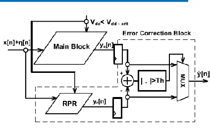
The ANT technique [2] includes both main digital signal processor (MDSP) and error correction (EC) block, as shown in Fig. 1. To meet ultralow power demand, VOS is used in MDSP. However, under the VOS, once the critical path delay Tcp of the system becomes greater than the sampling period Tsamp, the soft errors will occur. It leads to severe degradation in signal precision. In the ANT technique [2], a replica of the MDSP but with reduced precision operands and shorter computation delay is used as EC block. Under VOS, there are a number of input-dependent soft errors in its output ya[n]; however, RPR output yr [n] is still correct since the critical path delay of the replica is smaller than Tsamp [4]. Therefore, yr [n] is applied to detect errors in the MDSP output ya[n].
Fig 1: ANT architecture.
Error detection is accomplished by comparing the difference |ya[n] − yr [n]| against a threshold Th. Once the difference between ya[n] and yr [n] is larger than Th, the output ˆy[n] is yr [n] instead of ya[n]. As a result, ˆy[n] can be expressed as
Th is determined as
where yo[n] is error free output signal. In this way, the power consumption can be greatly lowered while the SNR can still be maintained without severe degradation.
III. Proposed ANT Multiplier Design
Using Fixed-Width RPR
A. Proposed Precise Error Compensation Vector for Fixed-Width RPR Design
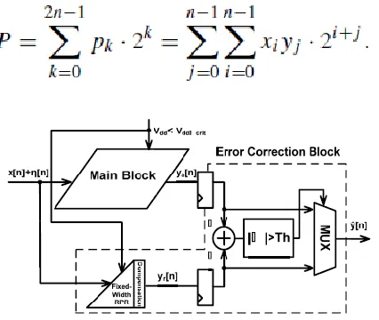
In the ANT design, the function of RPR is to correct the errors occurring in the output of MDSP and maintain the SNR of whole system while lowering supply voltage. In the case of using fixed-width RPR to realize ANT architecture, we not only lower circuit area and power consumption, but also accelerate the computation speed as compared with the conventional full-length RPR. However, we need to compensate huge truncation error due to cutting off many hardware elements in the LSB part of MDSP.
In the MDSP of n-bit ANT Baugh– Wooley array multiplier, its two unsigned n-bit inputs of X and Y can be expressed as
The multiplication result P is the summation of partial products of xiyj , which is expressed as
Fig 2 : Proposed ANT architecture with fixed-width RPR.
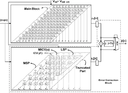
The (n/2)-bit unsigned full-width Baugh– Wooley partial product array can be divided into four subsets, which are most significant part (MSP), input correction vector [ICV(β)], minor ICV [MICV(α)], and LSP, as shown in Fig. 3. In the fixedwidth RPR, only MSP part is kept and the other parts are removed. Therefore, the other three parts of ICV(β), MICV(α), and LSP are called as truncated part. The truncated ICV(β) and MICV(α) are the most important parts because of their highest weighting. Therefore, they can be applied to construct the truncation error compensation algorithm.
To evaluate the accuracy of a fixed-width RPR, we can exploit the difference between the (n/2)-bit fixed-width RPR output and the 2n-bit full-length MDSP output, which is expressed as
where P is the output of the complete multiplier in MDSP and Pt is the output of the fixed-width multiplier in RPR. Pt can be expressed as
function contributed by minor input correction vector MICV(α).
Fig 3: 12 × 12 bit ANT multiplier is implemented with the six-bit fixed width replica redundancy block.
The source of errors generated in the fixed-width RPR is dominated by the bit products of ICV since they have the largest weight. In [8], it is reported that a low-cost EC circuit can be designed easily if a simple relationship between f (EC) and β is found. It is noted that β is the summation of all partial products of ICV. By statistically analyzing the truncated difference between MDSP and fixed-width RPR with uniform input distribution, we can find the relationship between f (EC) and β. As shown in Fig. 4, the statistical results show that the average truncation error in the fixed-width RPR multiplier is approximately distributed between β and β+1. More precisely, as β = 0, the average truncation error is close to β + 1. As β > 0, the average truncation error is very close to β. If we can select β as the compensation vector, the compensation vector can directly inject into the fixed-width RPR as compensation, which does not need extra compensation logic gates.
Before directly injecting the compensation vector β into the fixed-width RPR, we go further to double check the weight for the partial product terms in ICV with the same partial product summation value β but with different locations. As shown in Table I, the average error value for each ICV vector with the same partial product term summation value is nearly the same even their partial product term’s location is different. That is to say that no matter ICV = (1,0,0,0,0,0), ICV = (0,1,0,0,0,0), ICV = (0, 0, 1, 0, 0, 0), ICV = (0, 0, 0, 1, 0, 0), ICV = (0, 0, 0, 0, 1, 0), or ICV = (0, 0, 0, 0, 0, 1), their weight in each partial product term for truncation error compensation is nearly the same. Therefore, we apply the same weight of unity to each input correction vector element. This conclusion is beneficial for us to inject the compensation vector β into the fixed-width RPR directly. In this way, no extra compensation logic gates are needed for this part compensation and only wire connections are needed.
B. Proposed Precise Error Compensation Vector for Fixed-Width RPR Design
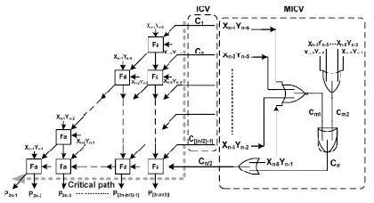
Fig. 9. Proposed high-accuracy fixed-width RPR multiplier with compensation constructed by the multiple truncation EC vectors combined ICV together with MICV.
The compensation vector ICV(β) is realized by directly injecting the partial terms of Xn−1Yn/2, Xn−2Y(n/2)+1, Xn−3Y(n/2)+2, . . . , X(n/2)+2Yn−2. These directly injecting compensation terms are labeled as C1,C2,C3, . . . ,C(n/2)−1 in Fig. 9. The other compensation vector used to mend the insufficient error compensation case is constructed by one conditional controlled OR gate. One input of OR gate is injected by X(n/2)Yn−1, which is designed to realize the function of compensation vector β. The other input is conditional controlled by the judgment formula used to judge whether β = 0 and βl ≠ 0 as well. In our presented fixed-width RPR design, the adder cells can be saved by half as compared with the conventional full-width RPR. Moreover, the proposed high-precision fixed-width RPR design can even provide higher precision as compared with the full-width RPR design.
IV.SIMULATION RESULTS
Simulated the existing and proposed system structures in Isim simulator. These results are developed for Spartan 3E FPGA Family kit by using Xilinx 14.5 software.
Area:
Timing Summary:
Minimum period: No path found
Minimum input arrival time before clock: 25.639ns Maximum output required time after clock: 10.918ns Maximum combinational path delay: No path found
RTL SCH:
Simulation Results:
Extension:
As an extension for this project we are implementing the multiplier in main DSP block using the DADDA multiplier so that area and power consumption is reduced.
V.CONCLUSION
In this paper, a low-error and area-efficient fixed-width RPR-based ANT multiplier design is presented. The proposed 12-bit ANT multiplier circuit is implemented in TSMC 90-nm process and its silicon area is reduced so that the power consumption is reduced. For the proposed extension with DADDA multiplier we further reduced the area and power compare to the proposed fixed width RPR for ANT Multiplier.
VI.REFERENCES
[1] V. Gupta, D. Mohapatra, A. Raghunathan, and K. Roy, “Low-power digital signal processing using approximate adders,” IEEE Trans. Comput. Added Des. Integr. Circuits Syst., vol. 32, no. 1, pp. 124–137, Jan. 2013. [2] B. Shim, S. Sridhara, and N. R. Shanbhag, “Reliable low-power digital signal processing via reduced precision redundancy,” IEEE Trans. Very Large Scale Integr. (VLSI) Syst., vol. 12, no. 5, pp. 497–510, May 2004.
[3] B. Shim and N. R. Shanbhag, “Energy-efficient soft-error tolerant digital signal processing,” IEEE Trans. Very Large Scale Integr. (VLSI) Syst., vol. 14, no. 4, pp. 336–348, Apr. 2006.
[4] R. Hedge and N. R. Shanbhag, “Energy-efficient signal processing via algorithmic noise-tolerance,” in Proc. IEEE Int. Symp. Low Power Electron. Des., Aug. 1999, pp. 30–35.