Execution of Low Power Optimizing Chien Search Usage
in the BCH Decoder
V. Sandeep kumar
Research Scholar, Department Of ECE
Sri Satya Sai University of Technology and medical sciences, Bhopal, MP
Abstract
—Designing multipliers that are high speed, low power, and regular design are of great interest to research. The multiplier speed can be increased by reducing the generated partial products. Many attempts have been made to reduce the number of partial products generated in the multiplication process, one of which is the multiplier of the matrix. The average sum of the matrix multiplier was used to summarize the transport products in a short time. The attainment of high-speed integrated circuits with low power consumption is a major concern for VLSI circuit designers. Most arithmetic operations are performed with a multiplier, which is the main element that consumes energy in digital circuits. In essence, the multiplication process is performed on hardware in terms of editing and adding. The adder optimization has led to improved multiplier performance. This project proposes a complete modified adder that uses a multiplexer to achieve a low power consumption of the multiplier. In order to analyze the efficiency of the proposed project, the conventional structure of the multiplier matrix is used. The designs are developed with Verilog HDL and the features are verified by simulation with Xilinx. In this project, the modified full adder that uses the multiplexer is compared to the traditional full hardware and speed adder.Keywords—
Array multiplier, Multiplexer, Full adder, Application Specific Integrated Circuit (ASIC).CHAPTER 1
I.INTRODUCTION
reduction tree using a probabilistic gate-level power estimator [6]. Because of this, switching power is reduced by optimizing transition activity in the partial product tree. In [7], partial product reorder is used to reduce the switching activity leading to power reduction. Partitioning the partial product tree into four groups and applying Dadda to a group and matrix multiplier to another, and so on, also achieves a power reduction [8]. In [9], a modified full adder using 4: 1 multiplexer is used in
1.
Existing Methods
1.1
Array Multiplier
The multiplier of the matrix is an efficient design of a multiplier multiplier. The multiplication of two binary numbers can be obtained by a microoperation using a combinational circuit that forms the product bit at one time, making it a quick way to multiply two numbers, since only the signal propagation time through the ports which forms the multiplication matrix. In the matrix multiplier, consider two binary numbers A and B, m and n bits. There is a synthesis that is produced in parallel by a set of AND gate. N x n multiplier requires n (n-2) full adder, n adder and n2 AND gate. Also, in the matrix multiplier, the worst case would be (2n + 1) td.
Figure 1.1 Array Multiplier
1.1.1
Conventional Full adder
Figure 1.2 Full Adder
1.1.2
MUX based Full adder
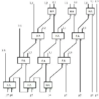
To reduce power and area, the full conventional adder in the matrix multiplier reduction step is replaced by a fully modified adder [9]. In the full MUX-based adder, the full adder is implemented using a 4: 1 multiplexer as shown in Fig. 3. Full MUX based adder implementation was achieved in reducing the power of the phase reduction of the Array multiplier. It is clear that a 4: 1 MUX can be done using three MUX 2: 1. The critical path delay can be written as shown below. The array multiplier can be made more efficient by further reducing the critical path delay. The same can be done using the complete summator proposed.
Delay = NOT + 2MUX
Figure 1.3. Full adder using six MUX
CHAPTER 2
LITERATURESURVEY
the energy delay timing product (TE), but the actual drawings include many TEs that are not on the critical path and this slack timing can be exploited using slower and lesser TE. Instead of optimizing delay and energy at the same time, critical TEs need to be optimized to reduce delay and non-critical TEs need to be optimized to reduce energy. For example, different structures have been used for critical and non-critical flip-flops in the context of a logical synthesis design stream.
LATCH AND FLIP-FLOP DESIGNS
stops and flip-flops used in this document. We limit our designs to completely static structures with minivan entrances and exits. When TEs have complementary outputs, we only load the selected output. We do not penalize the TE investment (eg PPCLA) because, in general, it is obviously not preferable to have a true or complementary production. To ensure the robustness of the design, the circuits must have input buffers to isolate input sources of any actively activated feedback node (for example, PTLA). In addition, for each TE project, we have dimensioned both low power
and high-speed versions, respectively identified by suffixes -lp and -hs
.
PPCLA [see Figure 1 (a)] is a transparent block based on the PowerPC design 603, which is known to be reasonably fast and low power [8]. PTLA [see Figure 1 (b)] is a steady-state transistor stopper, chosen for its low clock load. SSALA [see Figure 1 (c)] is a static differential differential locking device chosen for its low clock load. SSA2LA [see Figure 1 (d)] is a smaller variant of SSALA, with a higher load of the clock, but lower data transition energy when the clock is closed. CPNLA [see Figure 1 (e)] is PPCLA preceded by a pseudo-nMOS synchronized input buffer, which reduces the energy input transition when the stop is closed. When the latch is transparent, the p-transistor in the inverter clock acts as pseudo-nMOS load and dissipates so much static power when the data input is high.
CHAPTER 3
METHODOLOGY
Recently, many methods have been introduced to reduce the dynamic power of SoC systems. These methods, however, impose restrictive physical restrictions that have an impact on planning or are heavily dependent on logical functions such as clock synchronization.
This article features an elegant methodology that uses a pulsed flip instead of flip-flop without altering the existing design style. Reduces the dynamic power of the watch network, which can consume half the dynamic power of a chip.
Figure 1 — Pulse generator and waveform
CHAPTER 4
INTRODUCTION TO VLSI 4.1. INTRODUCTION TO VLSI
The abbreviation for VLSI is "very large range ICs". This is a combination of integrated circuits. The total frequency indicators of VLSI totaled hundreds of thousands of energies devices. Memorandum computer analogue or digital machine. Is a feature of VLSI Using backlink half-duplex technology, we can produce specific work chains and layout requirements. There are many projects that can create different circumstances or patterns in the communications system. In built-circuit design for creating chips and non-conforming of objects, layers on top of all other objects, the identities are also correct in layout settings.
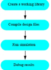
BASIC SIMULATION FLOW
Fig 4.8 flow of fundamental simulation
CHAPTER 5
INTRODUCTION TO XILINX
Migrating Projects from Previous ISE Software Releases:
However, you can create a backup copy of the original project as part of the project migration, as described below. To migrate a project
1. In the IE 12 Project Navigator, select File> Open Project.
2. In the Open Project dialog box, select the .xise file to migrate.Note You may need to modify the extension in the File Type field to view .npl (ISE 5 and ISE 6) or .ise (ISE 7 to ISE 10) project files.
3. In the dialog box that appears, select Backup and migration or migration only.
4. ISE software automatically converts the project into an ISE project 12.Note If you choose Backup and Migrate, a backup of the original project is created in project_name_ise12migration.zip.
5. Implement the project using the new version of the software. Note The distribution state is not retained after the migration.
RESULTS
2.1
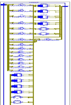
Implementing 4-bit Multiplier with conventional Full Adder
The 4-bit multiplier is implemented with the conventional full connector shown in Figure 2.2. The RTL scheme and the simulation waveform are shown in Figure 4.1 and Figure 4.2 below.
Figure 1.4. RTL schematic of 4-bit Array Multiplier using conventional Full Adder
Figure 4.7. Result of simulating the 4-batch array multipliers using the conventional full adder
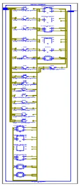
1.2 Implementing 4-bit Multiplier with proposed Full Adder
The 4-bit multiplier is implemented with the full summator proposed in Figure 3.1. The RTL scheme and simulation waveform are shown below in Figure 4.11 and Figure 4.12.
Figure 1.5. RTL schematic of 4-bit Array Multiplier using conventional Full Adder
Figure 1.6. Simulation result of 4-bit Array Multiplier using conventional Full Adder
The synthesis report in which the hardware required for 4bit- multiplier is shown below in fig 4.13.
CHAPTER 7
CONCLUSION& FUTURE WORK
The 4-bit matrix multiplier is implemented using the conventional sumer, the complete sumser based on mux, and the complete summator proposed. Of these three implementations, the proposed adder consumes less hardware than the device compared to other full adders.
The full adder can be replaced with parallel prefix adders to reduce hardware delay and complexity over these adders.
[2] S. R. Waters, E. E. Swartzlander, "A Reduced Wallace Reduced Complexity Multiplier", IEEE Transactions on Computers, vol. 59, n. 8, pp. 1134-1137, 2010.
[3] and Shahzad Asif Yinan Kong, "Low Area Wallace Multiplier", VLSI Design, vol. The 2014.
[4] MJ Rao, S. Dubey, "Booth High Speed and Efficient Harvest Area Wallace Multiplier Tree for Fast Arithmetic Circuits" at the Asia-Pacific Conference on Postgraduate Research in Microelectronics and Electronics (PrimeAsia), Hyderabad, India, 5-7 December 2012, pp.220-223.
[5] Karthick, Karthika S. and S. Valannathy, "Design and Analysis of Low Power Compressors", International Journal of Advanced Research Electrical Engineering and Electronics, and, Issue 6, December 2012.
![Figure 1 (d)] is a smaller variant of SSALA, with a higher load of the clock, but lower data transition energy when the](https://thumb-us.123doks.com/thumbv2/123dok_us/1966660.1259399/4.595.57.306.629.756/figure-smaller-variant-ssala-higher-clock-transition-energy.webp)