ABSTRACT
RONG, GUO. High Efficiency Charge Pump Based DC-DC Converter for Wide Input/ Output Range Applications. (Under the direction of Dr. Alex Q. Huang.)
Portable electronic devices are taking an indispensable part in people’s everyday life. To meet the growing needs of people, the number of function blocks inside the portable devices keeps on increasing but the portable devices tend to be small and exquisite. As a result, the power supply must be very compact and also very efficient during battery lifetime. Charge pump regulators are considered as an ideal solution in low power portable applications for their compact sizes and low cost. However, traditional charge pumps are not very efficient for battery powered applications because of the input voltage variations and the requirement for output regulation. The power rating of charge pumps is also very limited. A Multi-modes regulated charge pump with improved efficiency over wide input and load range is proposed. It can realize 2x, 1.5x, and 1.33x conversion modes. During each mode, the output voltage is regulated by a controlled current source. A hybrid control scheme is proposed. By using device segmentation control and pulse skipping modulation according to the load condition, the efficiency can be improved over a wide load range. Simulation and test results are provided to verify the control scheme.
a high performance one-fits-all power supply to avoid additional time and cost for re-design. Therefore, a power supply that can operate under a very wide input voltage range is a must for these applications. The most popular non-isolated step-down DC-DC converter, Buck regulator, usually shows a low efficiency at high input voltage. In addition, a high step-down ratio creates significant challenges for the PWM controller design because it has to control very narrow PWM pulses. A high efficiency charge-pump based wide input range Buck converter is proposed. The first stage is a multi-modes charge-pump and the second stage is a synchronous buck converter. The charge-pump is unregulated and adaptively switches between 1x, 0.5x, and 0.33x modes according to the input voltage. It does the rough voltage conversion while the Buck converter does the fine voltage regulation. Theoretical analysis proves that the total efficiency will be improved, especially at the high input voltage. It also simplifies the compensator design and benefits the transient performance. Experiment results show the highest efficiency improvement is 7% at heavy load and 16% at light load.
High Efficiency Charge Pump Based DC-DC Converter for Wide Input/Output Range Applications
by Rong Guo
A thesis submitted to the Graduate Faculty of North Carolina State University
in partial fulfillment of the requirements for the degree of
Doctor of Philosophy
Electrical Engineering
Raleigh, North Carolina 2010
APPROVED BY:
_______________________________ ______________________________ Dr. Alex Q. Huang Dr. William Davis
Committee Chair
DEDICATION
T
O MY PARENTSA
IZHUG
UO ANDL
AHUAD
ENGAND MY HUSBAND
BIOGRAPHY
ACKNOWLEDGMENTS
I would like to express my sincere appreciation to my advisor, Dr. Alex Huang, for his continued guidance, encouragement and support. Dr. Huang’s extensive vision, great intuition and accurate judgment have been the source of inspiration for my study and research in North Carolina State University in the past several years. It was an invaluable learning experience to be one of his students. The most precious things I have learned from him are the ability of independent research and also a careful research attitude.
I am grateful to my committee members, Dr. William Davis, Dr. Subhashish Bhattacharya, Dr. Srdjan Lukic for their valuable suggestions and help. Also I would like to thank Dr. Eunkyoung Shim for her service as the Graduate School Representative of my defense. The research work in this dissertation is supported by the Power Management Consortium of SPEC and also part of the research work is supported by RF Micro Device. I would like to give my special thanks to Mr. John Endredy in RF Micro Device who gave very valuable suggestions to this research work.
Han, Dr. Bin Chen, Dr. Jun Wang, Dr. Yu Liu, Dr. Jeesung Jung, Dr. Yan Gao, Dr. Wenchao Song, Dr. Tiefu Zhao, Dr. Jun Li, Ms. Juming Lai, Ms. Zhengping Xi, Mr. Jifeng Qin, Mr. Xiaohu Zhou, Mr. Gangyao Wang, Mr. Qian Chen, Mr. Woongje Sung, Ms. Zhan Shen, Mr. Zhuoning Liu, Mr. Sanzhong Bai and Mr. Edward van Brunt.
I appreciate the assistance from the staff members of the SPEC and FREEDM Systems Center, especially Mr. Anousone Sibounheuang, Ms. Colleen Reid and Ms. Karen Autry. I also would like to give my special thanks to Mr. Wenkang Huang and Mr. Richard Fitzpatrick in International Rectifier for their support and help during my preparation of this dissertation.
My heartfelt appreciation goes toward my parents, Aizhu Guo and Lahua Deng, who have always support and encourage me to pursue higher education.
TABLE OF CONTENTS
LIST OF TABLES ……… viii
LIST OF FIGURES ……….. ix
Chapter 1. Introduction ………. 1
1.1. Research Background ……… 1
1.2. Dissertation Outline ………... 6
Chapter 2. Characteristics of Existing Charge Pump Converters ………. 9
2.1. Inductor based vs. Charge Pump based DC-DC converter ………..…. 9
2.2. Topology of Existing Charge Pumps ……….… 18
2.3. Unregulated or Regulated Charge Pump ………...… 21
2.4. Summary ………..…. 26
Chapter 3. Design of A High Efficiency Regulated Charge Pump over Wide Input and Load Range for Portable Applications ……….. 28
3.1. Research Motivation ……….. 28
3.2. Regulation Scheme of Multi-modes Charge Pump ………... 30
3.3. Efficiency Improvement over Wide Input Range ……….. 39
3.4. Efficiency Improvement over Wide Load Range ……….. 42
3.5. System Stability Analysis ……….…. 47
3.6. Key Blocks Design ………...…. 61
3.7. Simulation and Experiment Verifications………..………. 69
Chapter 4. High Efficiency Multi-Modes Charge-Pump Based Buck Converter for
Wide Input Range Applications ………...…. 77
4.1. Research Motivation ……….…. 77
4.2. Proposed Structure of Wide Input Range Buck Converter ……… 79
4.3. Loss Break Down of Charge Pump ………...… 82
4.4. Loss Break Down of Synchronous Buck Converter ……….. 94
4.5. Efficiency Analysis of Charge-pump based Buck Converter ……… 100
4.6. Control Benefits of Charge-Pump based Buck Converter ………. 102
4.7. Experiment Verifications ………..…. 110
4.8. Summary ……… 112
Chapter 5. A High Efficiency Transformerless Step-up DC-DC Converter with High Voltage Gain for LED Backlighting Applications ………... 114
5.1. Introduction ……….... 114
5.2. Operation of Proposed High Gain Transformerless Step-up Converter…………. 116
5.3. Theoretical Efficiency Analysis ………. 119
5.4. Experiment Verifications ………... 126
5.5. Summary ………...…. 130
Chapter 6. Conclusions and Future Work ………. 132
6.1. Conclusions ……… 132
6.2. Future Work ………... 135
LIST OF TABLES
Table 1.1 Commercial Charge Pump Products……….. 3
Table 3.1 Output Impedance of Multi-Modes Charge Pump ………... 36
Table 3.2 Voltage of Flying Capacitors at Different Modes ………. 36
Table 3.3 The Voltage Swing of Nodes in Multi-Modes Charge Pump ……… 38
Table 3.4 System Poles of Charge Pump at Different Mode ……… 50
Table 3.5 Truth Table of Mode Decision ……….. 64
Table 3.6 Circuit Parameters for the Prototype ………. 73
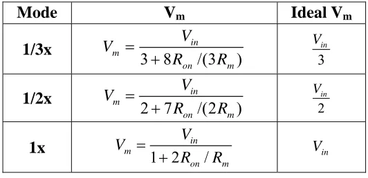
Table 4.1 Output Voltage of Charge Pump at Each Mode ……… 82
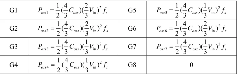
Table 4.2 Summary of Turn-on and Turn-off Losses ……… 92
Table 4.3 Summary of Coss Charging Loss ………... 92
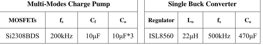
Table 4.4 Parameters of Circuit under Test ………... 110
Table 5.1 Topology Transformations of Multi-modes Step-up Charge Pump ………….. 118
Table 5.2 Output Equations for Each Stage ……….. 118
Table 5.3 Loss breakdown of Boost Converter ………. 121
Table 5.4 Loss breakdown of 3x mode Charge Pump ……….. 122
LIST OF FIGURES
Figure 1.1 A Ultra Slim Multi-Function Portable Device: IPad ………... 2
Figure 1.2 Efficiency Curves over Wide Input/Output Voltage Range and Load Range.. 5
Figure 2.1 Inductor Based DC-DC Converter ……….. 9
Figure 2.2 Typical Charge Pump Converters (a) Flying Capacitors OFF Chip (b) Flying Capacitors ON Chip ……….. 10
Figure 2.3 Demo Boards of a Boost Regulator and a Charge Pump Regulator ………... 11
Figure 2.4 SMT Inductors with Slim Outline ………... 12
Figure 2.5 Charge Pump ICs ……… 12
Figure 2.6 Transistor Size with Equal Current Driving Capability ……….. 14
Figure 2.7 Discharging Curve of a single Li-ion Battery ………. 15
Figure 2.8 Efficiency vs. Battery Voltage using Charge pump and Boost Converter …... 15
Figure 2.9 Noise profiles of inductor-based and charge pump converters……… 17
Figure 2.10 Five step-up SC converter topologies. (a) Dickson Charge Pump (b) Ladder. (c) Fibonacci (Makowski) (d) Series-Parallel. (e) Doubler ………. 19
Figure 2.11 1.5-times charge pump ………. 20
Figure 2.12 Two-phase Voltage Doubler ………. 21
Figure 2.13 Voltage Mode vs. Current Mode Charge Pump ……….… 22
Figure 2.14 Step-down Charge Pump (a) Schematic (b) Switch drive signals …………. 24
Figure 2.15 Schematic and Scheme of Pulse-Skip Regulation ……… 25
Figure 3.1 Topology of Multi-Modes Charge Pump ……… 30
Figure 3.2 Topology transformation of Multi-Modes Charge Pump ……… 31
Figure 3.3 Simplified DC model of Charge Pump ………... 32
Figure 3.4 Multi-Modes Charge Pump in 2x mode ……….. 34
Figure 3.5 Implementation of Multi-Modes Charge Pump in Transistor Level ………... 37
Figure 3.6 Dynamic Bulk Switching for PMOS ………... 38
Figure 3.7 Maximum Efficiency vs. VIN of Multi-Modes Charge Pump ……… 40
Figure 3.8 Hybrid Regulation Scheme for Improving Light Load Efficiency …………. 44
Figure 3.9 Key waveforms in hybrid regulation scheme ………. 45
Figure 3.10 Fast Light-Heavy Load Transient Response ………. 47
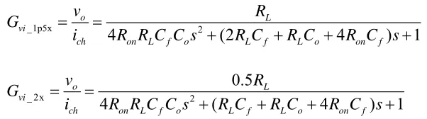
Figure 3.11 Equivalent small signal AC circuit model of Multi-Modes Charge Pump … 51 Figure 3.12 Comparison between Calculated and Simulated Gvi at 2x mode ………….. 52
Figure 3.13 Gvi at Different Input Voltage (Mode) ………... 54
Figure 3.14 Bode Plot of Gvi in 2x Mode at Different Load Current ………... 55
Figure 3.15 Bode Plot of Gvi in 2x Mode before and after Device Segmentation ……… 56
Figure 3.16 Modified Equivalent Circuit Model of 2x mode Charge Pump in PSM…… 57
Figure 3.17 Comparison between Calculated Gvi (Red) and Simulated Gvi (Blue)……... 59
Figure 3.18 Bode plots of Gvi in 2x Mode with (Red) and without (Blue) pulse skipping modulation……….. 60
Figure 3.19 Type III PID Compensator………. 61
Figure 3.21 Mode Change Control Logic………. 63
Figure 3.22 Universal Current Sensor ……….. 64
Figure 3.23 Device Segmentation and PSM Selector ……….. 67
Figure 3.24 Soft Start Control ………... 68
Figure 3.25 Load Transition from 50 mA to 500mA@ Vin=3.7V………. 70
Figure 3.26 (Left) Frequency vs. Load Current; (Right) Ripple vs. Load Current……... 70
Figure 3.27 Efficiency of Charge pump with Different Control Schemes at very Light Load Condition……….. 71
Figure 3.28 Efficiency of Designed Charge Pump at Different Load Currents………… 72
Figure 3.29 Test Bench of Designed Multi-modes Regulated Charge Pump……… 73
Figure 3.30 Test Results of Load Transitions from Very light->light->heavy load @ Vin=3.7V……… 74
Figure 3.31 Steady State at different load conditions when Vin=3.7V……….. 75
Figure 3.32 Total Loss Comparisons@ Iout=25mA……… 75
Figure 4.1 Proposed topology of wide input range DC-DC converter ………. 80
Figure 4.2 Comparisons of i1(t), v1(t), and vm(t) between simulation results and calculations ………... 88
Figure 4.3 Conduction Loss vs. Input Voltage in 1/3x Charge Pump (Po=10W) ………. 90
Figure 4.4 Turn on and Turn off Transients of the switches ……… 91
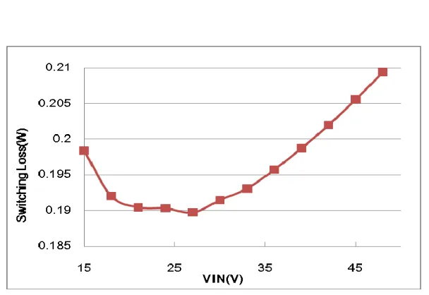
Figure 4.5 Switching Loss vs. Input Voltage in 1/3x Charge Pump(Po=10W) ………… 93
Figure 4.7 Conduction Loss vs. Input Voltage in Buck Converter (Vo=5V, Iout=2A) …... 96
Figure 4.8 Vds and Ids during Turn-On and Turn-Off of Switches ……… 96
Figure 4.9 Switching Loss vs. Input Voltage in Buck Converter (Vo=5V, Iout=2A) ……. 98
Figure 4.10 Losses vs. Input Voltage@Po=10W ……….. 99
Figure 4.11(a) Efficiency of Charge Pump at Different Modes ……….... 100
Figure 4.11(b) Efficiency of Buck converter with Different Input Ranges ……….. 101
Figure 4.12 Efficiency of Charge Pump based Converters vs. Vin………... 101
Figure 4.13 Comparison of Loop-Gain Variations over Wide Input Range between Single Voltage Mode Buck converter(Left) and Multi-modes Charge-Pump based Voltage Mode Buck Converter (Right)...………... 104
Figure 4.14 Block Diagram of Charge Pump Based Buck Converter in Voltage Mode ... 105
Figure 4.15 Comparison of Loop-Gain Variations over Wide Input Range between Single Current Mode Buck converter(Left) and Multi-modes Charge-Pump based Current Mode Buck Converter(Right)………... 107
Figure 4.16 Block Diagram of Charge Pump Based Current Mode Buck Converter …... 107
Figure 4.17 Inductor Current Ripple in Single Buck Converter (Red) and Multi-modes Charge Pump Based Buck Converter (Blue) ……… 108
Figure 4.18 Minimum Inductance of Single Buck Converter (Red) and Multi-modes Charge Pump Based Buck Converter (Blue) ……… 109
Figure 4.20 Tested Efficiency of Single Buck Converter and Multi-modes Charge
Pump based Buck Converter vs. Load Current ……… 112
Figure 5.1 Proposed Multi-modes Charge-pump based High gain Step-up DC-DC converter ………... 117
Figure 5.2 Duty Cycle vs. Gain ……… 119
Figure 5.3 Power Stage of Boost Converter ………. 120
Figure 5.4 Loss vs. Output Voltage (Boost Converter) ……… 121
Figure 5.5 Loss vs. Output Voltage (3x Mode Charge Pump) ………. 123
Figure 5.6 Efficiency vs. Output voltage @Vin=2.7V, Io=125mA ……….. 124
Figure 5.7 Minimum Inductance vs. Vo @Vin=2.7V, Io=125mA ……… 125
Figure 5.8 Designed High Voltage Gain Transformerless LED driver ………. 127
Figure 5.9(a) Node Voltages of Flying Capacitor Cf1……….. 128
Figure 5.9(b) Node Voltages of Flying Capacitor Cf2……….. 128
Figure 5.9(c) PWM Signals of Boost Converter and Charge Pump Converter………… 129
Figure 5.10 Duty Cycle vs. Output Voltage (Vin=2.7V, Iout=120mA) ……….. 129
Chapter 1. Introduction
1.1 Research Background
In people’s everyday lives, portable electronic devices are taking an indispensable part.
Most consumers own at least one mobile phone, and at least one other portable device, such
like digital camera, MP3 player, notebook, etc. As the name suggests, portable devices need
to be small in size and light in weight. In addition, as they are powered form batteries, it
requires that their voltage converter has high efficiency and low quiescent current so the
devices can be powered for a long time before needing to be recharged. Moreover,
consumers’ demands of multi-function portable devices become more and more intensive
nowadays. In stead of carrying three single-function portable devices, consumers tend to buy
a single device which integrates multiple functions. As a result, it brings great challenges to
the design of portable devices. A large number of function blocks inside a portable device
greatly increase the occupied space and the power consumption goes up as well. However,
the size of portable devices should be limited to maintain a fashionable outline. As a result,
Fig.1.1 A Ultra Slim Multi-Function Portable Device: IPad [1]
Inductor-based converters, usually with one or more inductors, and inductor-less
converters, also known as charge pumps [2], are two sorts of DC-DC converters that are
widely used for today’s portable power supplies.
Inductor-based converters can have very high efficiency over the entire battery voltage but
the cost and volume often make the engineers think twice. Charge pump regulators are
considered as an ideal solution due to their well-known compact sizes [3]. It first began with
unregulated ICs and then to regulated ICs with regulated output voltages. It eliminates the
use of inductor, thus reduces the cost and size. However, traditional charge pump, such as the
voltage doubler, is not very efficient for battery powered applications. The battery voltage
varies widely but the output voltage needs to be regulated to a fixed value [4]. The topology
of a charge pump sets a limit to the maximum efficiency it can achieve at one given input
voltage. Meanwhile, the regulation of charge pump converters is more lossy compared with
On the other hand, the power rating of charge pump converters is limited due to huge
conduction loss at high output current. In today’s market, there are hundreds of charge pump
ICs. Table 1.1 shows a statistics of commercial charge pump ICs from different Vendors.
Most of them can support power below 1W, but very few of them can support power above
2W. Conduction loss is a big concern when it is designed to be used in high power rating
because the charge pump has more transistors. If it is intentionally designed for high power
rating, big devices with low on-resistance must be used. However, light load efficiency will
suffer due to increasing switching loss.
Therefore, increasing the power rating and optimizing the efficiency of charge pump
converters over the entire battery life becomes a significant topic for designing the future
power supplies for portable devices.
Table 1.1 Commercial Charge Pump Products [15]
Vendor # of
ICs
Step-up ICs
LED driver
IC
Vin range Vout values Iout,max Pout,max
TI 70 44 1.8-3.6V, 2.7-5.4V,0.9-1.8V. 3.3V 5V, 0.3A 1.5W Linear
Tech 73 30 21 1.8-4.4V 2.7-5.5V 3.3V 5V, 0.5A 2.5W Maxim 50 17 1.8-5.5V 2.7-5.5V 3.3V 5V, 0.25A 1.25W
Fairchild 5 2 2.7-5.5V 3.3V, 4.5V,
5V 0.2A 1W
National 21 2 19 2.7-5.5 3.3V, 4.5V,
In automotive and telecommunication systems, which use backup batteries, the input
voltage variation is much wider than of portable applications, for example, 18-58V in an
automotive system [16]. In industry applications, the front-end bus voltage is relatively stable,
but can be selected from 12V, 24V, and 48V. Instead of redesigning the converter each time
when the bus voltage changes, customers may prefer a high performance one-fits-all power
supply to avoid additional development time and cost. Therefore, a power supply that can
operate under a wide input voltage range is a must for these applications. In addition to wide
input voltage range, the conversion ratio is another challenge when converting the highest
input voltage to the given low voltage bus. A high input-to-output step-down ratio creates
significant challenges for the PWM controller design because it has to control very narrow
PWM pulses. Meanwhile the converter switching frequency keeps on increasing to reduce
the size of inductors and capacitors. Therefore, the PWM pulses can become even shorter and
very difficult to control. For example, a Buck regulator with an input voltage of 66V and an
output voltage of 3.3V will require a duty cycle of approximately 5%. At a typical switching
frequency of 300 kHz, the required PWM on-time of the Buck switch is a mere 166 ns [17].
However, if the switching frequency increases to 2MHz, the on-time will be reduced to 25ns.
It is extremely demanding as it requires the switches have a very fast turn-on and turn-off
speed which limits the maximum frequency.
In addition, efficiency is always a target and needs to be as high as possible over the wide
input range. Since most of the converters are optimized at one operation point, the
variations of two commercial products with input, output voltage and load. It shows that the
efficiency difference can be 20%-30% at the same load when input or output voltage varies.
It is the switching loss that usually dominates the total loss when the input or output voltage
becomes high. Advanced devices can help reduce the switching loss, but the cost will go up.
(a) Buck Regulator (MAX5033) (b) Boost Regulator (MAX15031)
Fig.1.2 Efficiency Curves over Wide Input/Output Voltage Range and Load Range [18, 19]
A transformer based converter is a better choice to solve the above two issues. By utilizing
the turn-ratio of a transformer, extremely narrow duty cycles can be avoided. However
transformers are usually bulky and expensive if isolation is not required. Besides, core loss at
high frequency cannot be neglected.
As a result, it becomes very significant to research possible advanced topologies and
DC-DC converters.
1.2. Dissertation Outline
The dissertation consists of six chapters. They are organized as follows.
Chapter I. The background information and motivations of research are introduced.
Chapter II reviews the characteristics of existing charge pump converters. It starts with a
comparison between inductor-based converters and charge pump based converters, mainly
focusing on cost, size, efficiency, pin number, and output Noise. Then existing topologies of
charge pump circuits are reviewed. Although the topology differs, the basic cell is a voltage
doubler. A gain that equals to two is usually enough for portable applications; therefore the
voltage doubler becomes the base design of power supplies. Finally, the regulation methods
of charge pump converters are categorized and reviewed to provide references for designing
a regulated charge pump.
Chapter III proposes a high efficiency regulated charge pump over wide input (2.7-4.5V)
and load range (10mA-500mA) for battery powered applications. It adaptively changes the
conversion mode at different input voltage ranges. It also applies different control schemes to
different load conditions. A hybrid control scheme is proposed: When load decreases to light
condition, device segmentation control is used; When load further decreases, pulse skipping
complexity of control schemes, it is important to know if the system can remain stable over
the entire input range and load range. The small signal model and stability analysis for the
multi-modes charge pump are also derived to provide references for designing the
compensator. Key function blocks are explained in detail, including Mode Change Control
Logic, Universal Current Sensor, Device Segmentation and PSM Selector, and Soft Start.
Finally, a prototype is built to verify proposed control scheme. The experiment results show
that the total loss at light load can be reduced by 56% to 83%.
Chapter IV proposes a high efficiency multi-modes charge pump based Buck converter for
wide input range applications. An unregulated multi-modes charge pump is used as a
pre-regulator of a standard buck converter and does the rough voltage conversion. According
to the input voltage, the charge pump can adaptively select the best mode to step down the
input voltage. The input voltage range of Buck converter is greatly reduced and therefore low
cost device can be used. Since the Buck converter and the charge pump converter exhibit
different efficiency tendencies within the same input range, it is proved that the total
efficiency can be improved by combining them, especially at high input voltage. Theoretical
efficiency analysis and comparisons between multi-modes charge pump and synchronous
Buck are given. On the other side, the fine regulation of output voltage is achieved by the
Buck converter. Now the duty cycle will not become extremely low because the input voltage
range of Buck converter becomes more centralized after the charge pump. It also directly
benefits the compensator and output LC filter design of Buck converter. A 10W prototype is
efficiency improvement is 7% at heavy load and 16% at light load.
Chapter V proposes a high efficiency transformerless Step-up DC-DC Converter with high
voltage gain for LED Backlighting applications. To overcome the shortage of low efficiency
when increasing the number of LEDs that a single Boost converter is driving, a multi-modes
charge pump is cascaded with the Boost converter. Using the similar concept shown in
chapter IV, the efficiency can be improved by changing the mode of charge pump according
to the number of LEDs in series.
Chapter VI summarizes the present work and proposes the future work regarding the
Chapter 2. Characteristics of Existing Charge
Pump Converters
2.1 Inductor based vs. Charge Pump based DC-DC converter
Nowadays, the most widely used approach to perform DC to DC conversions is
inductor-based DC-DC converters, which includes at least one inductor. For low-power and
highly integrated electronic systems, inductor-based converters usually have the switches
integrated with the controller. Fig.2.1 shows the typical configuration of inductor-based
DC-DC converter. The way how the inductor is connected can result in different topologies.
Buck, Boost, and Buck-Boost Converter are three general DC-DC converters that are used in
portable applications.
As an alternative of inductor based converters, charge pump based converters can also
perform DC-DC conversion, but with only switches and capacitors. Compared with an
inductor-based converter, it stores energy in capacitors instead of inductors. Different
arrangement of capacitors and switches can result in different voltage gains, such as voltage
doubler, divider, inverter, and etc. Basically, charge pump circuits utilize flying capacitors
with their bottom plates connected to a voltage pulse signal. The flying capacitor can be seen
as a voltage source with a constant voltage VCf if it is sufficiently large. As a result, the
voltage of top plate will change with the bottom plate but one VCf higher or lower. From this
point of view, the maximum voltage we can get from a voltage doubler will be only two
times the battery voltage. Depending on the power rating, charge pump converter can be
partially integrated or fully integrated. Fig.2.2 (a) is the configuration of a charge pump
converter without integrating the flying capacitors while Fig.2.2 (b) shows a fully integrated
charge pump converter.
Fig.2.2 Typical Charge Pump Converters (a) Flying Capacitors OFF Chip (b) Flying
It is often controversial in selecting either inductor-based topology or Charge Pump-Based
topology before designing the power supply for portable devices. Therefore, it is very
important to know the advantages and disadvantages of both.
Fig.2.3 Demo Boards of a Boost Regulator and a Charge Pump Regulator [20]
1) Cost and Size
In inductor-based DC-DC converter, it is the inductor that usually dominates the cost and
size. In portable applications, the inductor used in a DC-DC converter usually can take 2-5
times more area than that of the regulator IC. Moreover, it is usually at least 2 times thicker
than the regulator IC. Although the switching frequency has been greatly increased in today’s
power supplies and more compact designs of SMT inductors become available, it is still not
easy for the inductors to be integrated on chip or even packaged within chip. Fig.2.4 shows
the dimension of compact SMT inductors from CoilCraft. In addition, the cost of high
performance inductor with low DCR usually is not cheap. Engineers tend to use cheaper
Fig.2.4 SMT Inductors with Slim Outline [21]
On the other hand, the availability of high value multi layer ceramic capacitors makes the
charge pump converter a strong competitor of the inductor-based DC-DC converter. The
charge pump converter only includes several ceramic capacitors besides of the regulator IC.
Compared with inductor based converters, for a given output capacity, the flying capacitors
in charge pump converters are roughly 5 to 10 times less expensive than the inductor, and
also 5 to 10 times smaller [3].
With output power below 100mW, fully monolithic charge pump converters with flying
capacitors on chip are already commercialized. Packaging the flying capacitors with the
silicon chip is an alternative way of integration. Fig.2.5 shows the profile of charge pump ICs
for mobile applications from National Semiconductor. Both ways form an ultra integrated
solution for the voltage conversion in portable devices. The regulator then only needs one
external output capacitor.
2) Efficiency
Inductor-based converters are usually considered more efficient for voltage conversion
than charge pump converters. For example, a Boost converter only needs two switches, but a
voltage doubler needs four switches, two at each side of the flying capacitor. Therefore,
within limited chip area, the current paths in a charge pump converter are much more
resistive than that in an inductor-based converter. When load current increases, the
conduction loss goes up quickly and efficiency decreases. However, with advanced process
technology, the charge pump can almost compete with inductor-based converters. The
innovations in process technology make MOSFETs available with very low resistance per
Fig.2.6 Transistor Size with Equal Current Driving Capability [23]
On the other hand, unlike inductor-based converters, the maximum efficiency of charge
pump converters highly depends on their structures and input voltages. For example, a
voltage doubler can have a 95% efficiency when the input voltage is around half of the
output voltage, but the efficiency can decrease to less than 50% when the input voltage is
equal to the output voltage. This is very bad because the voltage of a typical battery changes
during its discharging cycle, as shown in Fig.2.7. However, multi-modes charge pump
products are now available and can provide an average efficiency similar to inductor-based
converters over a typical battery voltage range. It can adaptively select the proper conversion
mode to achieve the best efficiency according to the ratio of output voltage to input voltage,
as shown in Fig.2.8. In today’s market, charge pump ICs with two conversion ratios are very
popular. Very few ICs that use three flying capacitors to achieve four conversion ratios are
Fig.2.7 Discharging Curve of a single Li-ion Battery [24]
3) Pin Number
For inductor based converters, it generally requires at least four pins: Input voltage,
Inductor connection, Feedback Voltage, and ground, which can be seen from Fig.2.1. In
practical, an Enable pin is often added. For charge pump converter, the pin numbers can vary
a lot. It can be seen from Fig.2.2: if it is a fully integrated charge pump or with flying
capacitors packaged inside, it only requires three pins: Input voltage, Output Voltage, and
ground, which is less than inductor based converter; if flying capacitors are out of package,
then it needs four more pins in addition to the original three pins for flying capacitor
connections. However, pin numbers can be even more depending on the current capacity,
conversion ratio and additional features. Therefore, it is obvious that low current charge
pump converters have less pin numbers while high current charge pump converters have
more pin numbers than inductor based DC-DC converter.
4) Output Noise
Theoretically, there are plenty of noise sources in a switching power supply. However,
intrinsic noise which is generated by the regulator itself is considered dominant compared to
any other noise sources [3]. The switching nature of inductor-based and charge pump
converters are different. One uses inductors to store energy while the other uses capacitors to
store energy. Fig.2.9 shows the noise profiles of the inductor-based and charge pump
converters. It can be seen that both converters show output noise around switching frequency
and its harmonics. However, for inductor-based converters, additional noise is introduced by
video frequency range in portable applications. Reducing the amplitude of switching intrinsic
noise can be done by increasing the output capacitor value, but this will also shift more
deeply the LC filter resonance frequency into the sensitive audio band [3].
On the other hand, the inductor on a PCB board can be considered as an antenna and emit
electromagnetic waves when the converter is switching. The Electro-magnetic interference
(EMI) may cause other sensitive circuits nearby to fail to work correctly. Therefore, the EMI
issue is a big limitation for an inductor-based converter to be used in RF and audio
applications. Shielded inductors are often used to reduce the EMI; however it definitely
further increases the cost and weight.
Fig.2.9 Noise profiles of inductor-based and charge pump converters [3]
converters are equally able to meet all the requirements of portable devices. It has low weight,
low cost, small size, and comparable efficiency over variable input voltage range with the
inductor-based converter. Moreover, it generates less noise, which is good for noise sensitive
circuits in portable devices.
2.2 Topology of Existing Charge Pumps
A number of charge pump circuit topologies exist in the literature [2][7][10][12][26-28],
such as Dickson charge pump, Ladder, Makowski charge pump, Series-Parallel Charge pump,
Voltage doubler, and so on. Fig.2.10 shows the topologies of five step-up charge pump
circuits. Each of them uses three flying capacitors, but the switch number and the maximum
gain may be different. The merits of each topology are given in [9]. It seems that there are
lots of topologies to select, but it actually highly depends on the respective application. For a
charge pump that targets portable applications, it mostly needs to step up the battery voltage
(2.7-4.5V) to 5V. Therefore, a maximum gain of 2 is already enough. It can be seen from
Fig.2.10 that the basic cell of the five charge pump topologies is the same, which is a voltage
doubler, as shown in the red block. Therefore, a voltage doubler becomes the base design for
(a) Dickson Charge Pump (b) 1:4 Ladder
(c) 1:5 Fibonacci (Makowski) (d) 1:4 Series-Parallel
(e) 1:4 Doubler
Fig.2.10 Five Step-up SC Converter Topologies. (a) Dickson Charge Pump (b) Ladder. (c)
Load COUT
CF1 CF2
S1 S2 S3
S4
S5 S6 S7
VIN
IIN
IOUT
VOUT
OSC CONTROL
Fig.2.11 1.5-times charge pump [13]
Based on the principal of a voltage doubler, several other charge pump topologies can be
derived, such as 1.5-times charge pump, 1.33-times charge pump, multi-phase voltage
doubler, and so on. Fig.2.11 shows the topology of a 1.5-times charge pump. Similar to a
voltage doubler in structure, but the flying capacitors are charged in series to 0.5 times the
input voltage in a 1.5-times charge pump. Fig.2.12 shows an interleaving two-phase voltage
doubler. In this topology, two charge pumps are connected in parallel but operate with 180°
phase shift angle. When the duty cycle is set to 50% for both charge pumps, the output
current is therefore continuously supplied from the input, thus reducing the ripple to a
Load COUT
CF1 CF2
S11 S12
S13 S14
S21 S22
S23 VIN
IIN
IOUT
VOUT OSC
CONTROL
S24
0º 180º
Charge Pump #1
Charge Pump #2
Fig.2.12 Two-phase Voltage Doubler [13]
2.3 Unregulated or Regulated Charge Pump
Depending on the application, a charge pump converter can be regulated or unregulated.
When it is unregulated, the output varies with input and delivers a multiple of the input
voltage. In portable applications, it often requires charge pump to transform the decreasing
voltage of a discharging battery into a stable supply. Therefore, regulation is required for
charge pump converters. Generally, the regulation schemes can be summarized to two
categories according to the switching frequency: constant frequency regulation and variable
2.3.1 Constant Frequency Regulation
1) Voltage Mode Control
The regulation scheme using voltage Mode Control is usually achieved by controlling the
on-resistance of a single or multiple switches in either the charging or discharging path. As
the on-resistance of switch is regulated, the voltage drop across the switch is controlled. An
error amplifier compares the output voltage against a reference voltage, and feeds back an
error signal to the on-resistance control block, as shown in Fig.2.13 [5]. For low load current
or high input voltage, the on-resistance will be increased and consume the excessive voltage;
for high load current or low input voltage, the on-resistance gets smaller. The duty cycle of
charging and discharging phase is fixed to 50%. The biggest advantage of this method is
fixed frequency operation with a very low output voltage ripple that makes filtering easier.
2) Current Mode Control
Instead of regulating the on-resistance, the current mode regulation controls the current
flowing through the switch. Therefore, the regulated switch operates as a controlled current
source instead of a variable resistor, as shown in Fig.2.13. The current source can be either
located in the charging path [14] or discharging path [5]. When the current source is placed in
the charging path, the charging current of flying capacitor is controlled thus the voltage
across the capacitor is regulated. It is easier to regulate M2 since its source is connected to
the ground instead of floating. Similar to this, when the current source is located in
discharging path, M3 is usually easier to be regulated than M4. Same with voltage mode
control, the duty cycle of charging and discharging phase is also fixed to 50%.
3) Pulse Width Modulation (PWM) [11, 29]
Another regulation scheme of charge pump with constant frequency is PWM control.
Instead of fixing the duty cycle to 50% in current and voltage mode, the duty cycle will
change with the input voltage and load current. Fig.2.14 shows a regulated step-down charge
pump using PWM control. The output voltage Vo is fed back to the error amplifier and
compensation circuit. Then the output of compensator will be compared with a sawtooth
waveform and generates desired duty cycle. Finally, the logic circuit will convert the duty
cycle signal to gate driving signals for the four switches in the charge pump. By controlling
the duty cycle, the average energy that charge pump delivers to the load is controlled and
thus the output voltage can be regulated. The biggest drawback of PWM regulation is that it
Fig.2.14 Step-down Charge Pump (a) Schematic (b) Switch drive signals.[11]
2.3.2 Variable Frequency Regulation
1) Pulse-Skip Regulation
In pulse-skip regulation, the output voltage is regulated by skipping unneeded pulses. If
output voltage is lower than the reference voltage, the charge-pump continuously switches
and charges the output capacitor. If the output voltage exceeds the reference voltage, the
charge pump stops and no energy will be provided through the charge pump. The regulation
scheme is shown in Fig.2.15. The advantage of this regulation is the low average control
current, especially at light load condition since the charge pump stops operation most of the
time. The disadvantages are wide frequency variations and higher output voltage ripple
(a) Schematic of Charge Pump with Pulse-Skip Modulation [8]
(b) Typical scheme of Pulse-Skipping Regulation [13]
2) Linear Skip Regulation
To improve the output voltage ripple at pulse skip modulation, an improved control
‘Linear Skip Regulation’ (Fig.2. 16) is proposed by [29]. LinSkip regulation uses 3 phases,
charge phase, transfer phase and wait phase. During the wait phase, the charge pump stops
operation and the load current is only supplied by the output capacitor. In addition to pulse
skipping, this scheme also regulates the current transferred to the output. If load current is
high, there will be no wait phase and the frequency is fixed. Only the current transferred per
cycle is regulated. If load current is low, the current is fixed but the duration of wait phases is
regulated, similar to pulse skip modulation.
Fig.2.16 Scheme of Linear-Skip Regulation [29]
2.4. Summary
In order to know the strength and weakness of charge pump converters and see how they
DC-DC converters and charge pump converters was presented in this chapter. For portable
application, charge pump DC-DC converters beat the inductor-based converter with lower
weight, lower cost, smaller size, and comparable efficiency. Popular topologies and control
schemes of charge pump converters were also briefly reviewed to make the basis for the
Chapter 3. Design of A High Efficiency
Regulated Charge Pump over Wide Input and
Load Range for Portable Applications
3.1 Research Motivation
In DC-DC converters, charge pump regulators are well known for their compact sizes
since they do not have large and expensive magnetic components. Unlike LDO regulators,
which can only step-down the input voltage, charge pump regulators can either boost or buck
the input voltage by using different topologies. As a result, charge pump regulators are
usually considered as an ideal solution in low power portable applications.
However, the traditional charge pump, like a voltage doubler, is not a good solution for
applications where the input (Battery) voltage varies a lot, and the output voltage needs to
remain regulated. It only has high efficiency when desired output voltage is close to two
times input voltage. The power loss will be particularly high when the input voltage is close
to the output voltage. Multi-Modes Charge Pumps were proposed by researchers to improve
the efficiency over wide input range. By alternating the connections between switches and
flying capacitors during charging and discharging period, multiple conversion ratios can be
can be regulated using on-resistance regulation, duty cycle modulation, etc [13].
On the other side, when a charge pump needs to operate over a wide load range, the light
load efficiency is important, especially for applications, such like cell phones, which mostly
work in standby mode. Normally, the devices’ sizes are optimized to reduce conduction loss
and maintain regulation at maximum load; therefore, they are big devices with small
on-resistance. However, small on-resistance will not contribute to the light load efficiency
because the conduction loss is not dominant anymore. On the contrary, those big devices still
need a lot of power to drive them since the gate driver loss does not scale down with the load
current. In order to improve the light load efficiency, the driving loss needs to be as low as
possible. This is also true for inductor-based DC-DC converters. Many solutions have already
been proposed, by using either advanced control or improved power stage, such as pulse
frequency modulation, pulse skipping modulation, device segmentation, etc [35-49].
A high efficiency regulated Multi-Modes Charge Pump over wide input and load range is
proposed. The input is a single Li-ion battery with voltage between 2.7V and 4.5V, while the
output voltage needs to be regulated to 5V. The charge pump can automatically adjust the
conversion modes: 2x, 1.5x, and 1.33x according to different input voltages, therefore
enhance the average efficiency over the entire battery life. The maximum load current is
500mA, but can go as low as 10mA. When the load current decreases to light load condition,
device segmentation control is used; and when the load further decreases, pulse skipping
modulation will be used in addition to the device segmentation. By using proposed hybrid
control scheme, the gate driver loss and switching loss at light load can be greatly reduced,
3.2 Regulation Scheme of Multi-Modes Charge Pump
Ideally the efficiency of a charge pump can be approximated by (3.1) if the gate driving
loss, switching loss and quiescent loss are neglected. N is the mode conversion ratio. It can
be seen that the maximum efficiency it can achieve is limited by its topology. If it is a voltage
doubler, N=2 and the maximum efficiency at any input voltage will be equal to Vout/2Vin.
out
in
V
V N
η =
∗ (3.1)
When Vin gets close to 0.5 Vout, the maximum efficiency is close to 1; When Vin is much
higher than 0.5Vout, the efficiency will become very low; When Vin is lower than 0.5Vout, the
output will be out of regulation. Therefore, the efficiency varies with input voltage when the
topology is fixed. To achieve a high efficiency over wide input range, a simple voltage
doubler certainly cannot meet the requirement. Instead, Multi-Modes Charge Pump which
can adaptively change the mode according to the input voltage will be a good solution.
Fig.3.1 shows the topology of a Multi-Modes Charge Pump.
C
Chhaarrggiinngg[[00--00..55TTss]] DDiisscchhaarrggiinngg[[00..55TTss--TTss]]
Fig.3.2 Topology transformation of the Multi-Modes Charge Pump
Three different conversion ratios can be realized by alternating the arrangement of
switches and capacitors. Take Mode 1.33x as the example. During [0-0.5Ts], G1, G5, G6, and
G10 are ON while G2, G3, G4, G7, G8, and G9 are OFF. Flying capacitor Cf1, Cf2, Cf3 are 1.33X Mode
1.5X Mode
in series connection and being charged by the input source Vin; during [0.5Ts-Ts], G1, G5,
G6, and G10 are OFF while G2, G3, G4, G7, G8, and G9 are ON. The branch circuits of Cf1,
Cf2 and Cf3 are in parallel connection and discharge energy to the output. The output voltage
therefore is the sum of Vin and the voltage across the flying capacitor. The topology
transformation of Mode 1.33x, Mode 1.5x and Mode 2x in one cycle are shown in Fig.3.2.
Fig.3.3 shows a simplified DC model of charge pump without considering gate driver loss,
switching loss and leakage loss. Rout is the output impedance of charge pump. When Vout is
not regulated, Rout is fixed. Therefore, Vout is close to N*Vin and changes with Vin. When
output needs to be regulated, Rout will vary with Vin, load current Iout, and mode conversion
ratio N, as shown in (3.2).
Fig.3.3 Simplified DC model of Charge Pump
out in out out
V = ∗N V −I ∗R (3.2)
There are two ways to regulate the output of charge pump. One is Constant Frequency
Mode Regulation. The output voltage is regulated using error amplifier by controlling either
the on-resistance of transistors or duty cycle. Since switching frequency is fixed, the output
voltage ripple and the size of output capacitor can be reduced. The main drawback is high
Regulation. A hysteresis comparator is used to control the on and off of switches according to
the output voltage variation. It does not need any amplifier or compensator and it can have
high bandwidth and fast transient response. It also has low quiescent current which is good
for light load efficiency. However, it has high output ripple and variable ripple frequency
which is not easy for the following filter design.
A good compromise is to combine the two regulation technique so that a trade off the
ripple and efficiency can be achieved.
Comparing the methods of constant frequency regulation, regulating the on-resistance of
switches while the duty cycle is fixed to 50% is preferred than regulating the duty cycle
while the on-resistance is fixed. It will be difficult to control narrow duty cycle when N*Vin
is much higher than desired Vout. The maximum frequency is therefore limited.
Generally, there are two options when selecting the transistors that will be regulated. One
is regulating the transistors in charging path and the other is regulating the transistors in
discharging path.
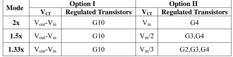
For Option I, only the on-resistance of transistor G10 in the charging path is regulated.
Transistors G1-G9 will have fixed on-resistance. Assume G1-G9 have equal on-resistance
Rsw, while the impedance of regulated transistor G10 is Rt. All capacitors have the same ESR.
The DC output impedance of charge pump can be derived according to its loss dissipation.
Taking Mode 2x as the example. The charging and discharging paths of the Multi-Modes
Charge Pump in 2x mode are shown in Fig.3.4. In order to maintain the charging balance, the
integration of the current through Cf3 in one cycle should be: <ICf3>Ts=0. Since duty cycle is
equal, as: ICharge=IDischarge. Similarly, the average value of charging and discharging current
through output capacitor Cout should also be equal, as: Iout=IDischarge-Iout. Therefore,
ICharge=2Iout. The transistor conduction loss PCon, flying capacitor loss PCf, and ESR loss PESR
can be derived using (3.3), (3.4), and (3.5). The total loss is the sum of conduction loss of
transistors, flying capacitors and ESR, gate driver loss and leakage loss, as shown in (3.6).
Ultimately, the DC impedance of Charge pump can be obtained, as shown in (3.7).
Fig.3.4 Multi-Modes Charge Pump in 2x mode
Model 2x:
Loss in switches: (2 )2 2 (2 )2 0.5 4 2 (2 0.5 )
Con out SW out t out SW t
P = I × R + I R × = I × R + R (3.3)
Loss in flying capacitors: 2/ f
C out s f
P =I f C (3.4) Loss in ESR: (2 )2 2
ESR out out
P = I ×ESR+I ×ESR (3.5)
Total Loss: ( ) 2
f
Total Con C ESR q IN gate out out q IN gate
P = P +P +P +I V +P =R I +I V +P (3.6)
8 5 1/( ) 2
out SW s f t
Similarly, we can derive the losses and Rout for Mode 1.5x and 1.33x.
Mode 1.5x:
Loss in switches: 2 (3.5 0.5 )
Con out SW t
P =I × R + R (3.8)
Loss in flying capacitors: 2/(2 )
f
C out s f
P =I f C (3.9) Loss in ESR: 3 2
ESR out
P = I ×ESR (3.10)
Total Loss: 2 3.5 3 1/(2 ) 0.5
Total out SW s f t q IN
P =I ⎡⎣ R + ESR+ f C + R⎤⎦+I V (3.11)
3.5 3 1/(2 ) 0.5
out SW s f t
R = R + ESR+ f C + R (3.12)
Mode 1.33x:
Loss in switches: 2 (2 0.22 )
Con out SW t
P =I × R + R (3.13)
Loss in flying capacitors: 2/(3 )
f
C out s f
P =I f C (3.14)
Loss in ESR: 2 2.33
ESR out
P =I × ESR (3.15)
Total Loss: 2 2 2.33 1/(3 ) 0.22
Loss out SW s f t q IN
P =I ⎡⎣ R + ESR+ f C + R⎤⎦+I V (3.16)
2 2.33 1/(3 ) 0.22
out SW s f t
R = R + ESR+ f C + R (3.17)
For Option II, the on-resistance of transistors G2, G3, and G4 located in the discharging
paths are regulated; Transistors G1 and G5-G10 have fixed resistance. Using the same
method, the output impedance of charge pump at each mode for Option II can be derived.
The results of Option I and Option II are shown in Table 3.1. Once Rsw, ESR, and
Table 3.1 Output Impedance of Multi-Modes Charge Pump
It can be seen that option II can more efficiently regulate the charge pump since the control
gain from Rout to Rt are larger. However, input current spike during mode change can be huge
since the voltage across flying capacitors has a sudden change during mode change, which
are shown in Table 3.2. Besides, the voltage run-away can happen among the flying
capacitors since they are not in direct parallel with each other during the discharging phase.
Compared with Option II, Option I is free of such two issues.
Table 3.2 Voltage of Flying Capacitors at Different Modes
Finally, Option I is adopted in this design: only regulating transistor G10 in the charging
path. The implementation of Multi-Modes Charge Pump is shown in Fig.3.5. To avoid
Mode Option I Option II
VCf Regulated Transistors VCf Regulated Transistors
2x Vout-Vin G10 Vin G4
1.5x Vout-Vin G10 Vin/2 G3,G4
1.33x Vout-Vin G10 Vin/3 G2,G3,G4
Mode Output Impedance (Rout)
Option I Option II
2x 8Rsw+5ESR+1/(fsCf)+2Rt 8Rsw+5ESR+1/(fsCf)+2Rt
1.5x 3.5Rsw+3ESR+1/(2fsCf)+0.5Rt 3Rsw+3ESR+1/(2fsCf)+Rt
floating driving issues, G1-G9 are implemented using PMOS, denoted as MP1-MP9. The
gate voltage of MP1-MP9 fully swings from ground to Vout(5V), so they are unregulated.
G10 is implemented using NMOS, denoted as MN1. The output voltage Vout will be
compared with desired reference voltage and the error will be integrated by a PID
compensator. When MN1 is ON, the gate voltage is equal to the output voltage of
compensator Vc; When MN1 is OFF, the gate voltage is zero. Therefore, the gate driving
voltage of MN1 swings from ground to Vc. It is worth to clarify that the PID compensator
controls the gate voltage of MN1, so it may drive MN1 either in saturation or linear region.
Generally, MN1 is in saturation region when the impedance needs to be large and in linear
region when the impedance needs to be low. However, no matter if it is in linear or saturation
region, the regulation principle can still be explained using the same DC model.
Table 3.3 The Voltage Swing of Nodes in Multi-Modes Charge Pump
Mode n1 n2 n3 n4 n5 n6
2X Vin Vin Vin Vin Vin ~Vout gnd~Vin
1.5X Vin Vin Vin~Vout 1/2Vin~Vin 1/2Vin~Vout gnd~Vin
1.33X Vin~Vout 2/3Vin~Vin 2/3Vin~Vout 1/3Vin~Vin 1/3Vin~Vout gnd~Vin
The voltage swing of nodes n1-n6 at different mode is shown in the Table 3.3, which will
be the reference to connect the bulk of each transistor correctly. For MP2, MP3 and MP4, it
can be seen that nodes n2, n4 and n6 are always less than the node Vin. Therefore, the bulk
should be connected to Vin. For MP7, MP8, and MP9, nodes n1, n3, and n5 are always less
than the nodes Vout. Therefore, their bulk should be connected to Vout. For MN1, the bulk is
connected to ground. However, for MP1, MP5, and MP6, the comparison of voltage between
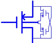
both ends is complicated since the result is not consistent when the mode changes. Dynamic
Bulk switching technique is proposed by some researchers to solve this problem [50]. Fig.3.6
shows the structure of a PMOS with dynamic bulk switching. The bulk of targeted PMOS
will be adaptively connected to the higher voltage between source and drain by adding
another two small PMOS across both ends.
3.3 Efficiency Improvement over Wide Input Range
Eq.(3.1) shows that the maximum efficiency of charge pump at given input voltage is
determined by its topology. For example, when input voltage is 3.9V, the maximum
efficiency of charge pump is 5/(2*3.9)=64.1% in 2x mode, 5/(1.5*3.9)=85.5% in 1.5x mode,
and 5/(1.33*3.9)=96.4% in 1.33x mode. Therefore, working at the right operation mode for
given input voltage will greatly benefit the efficiency.
In a Multi-Modes Charge Pump, the mode can be easily changed by re-arranging the
connection of switches and capacitors according to the input voltage. It is important to know
the proper range of Vin for each mode. Fig.3.7 shows the Efficiency variations of
Multi-Modes Charge Pump over the entire battery voltage range. The x-axis is weighted
according to the discharging curve of lithium-ion battery. The dotted line is the minimum
voltage that the charge pump can stay in the lower conversion ratio modes. However, the real
mode transition point should be selected higher than the minimum voltage considering the
voltage drop on charge pump itself. In Fig.3.7, it can be seen that Eff1<Eff2<Eff3 over the
entire input range. As a result, when pushing the transition points to higher input voltage, the
average efficiency will degrade. On the other side, since the output voltage is regulated to the
same value during each mode, it should meet inequalities (3.18)-(3.20).
2X: 1.5Vin -Rout _min(1.5x)*Iout≤ Vout≤ 2Vin - Rout _min (2x)*Iout (3.18)
1.5X: 1.33Vin - Rout _min (1.33x)*Iout≤ Vout≤ 1.5Vin - Rout _min (1.5x)*Iout (3.19)
0.6 0.65 0.7 0.75 0.8 0.85 0.9 0.95 1
4.50 4.20 4.00 3.90 3.85 3.80 3.75 3.70 3.65 3.60 3.55 3.50 3.40 3.30 2.70
Max
im
um
Ef
fici
ency
VIN(V)
Maximum Efficiency vs. VIN
Eff1 Eff2 Eff3
Fig.3.7 Maximum Efficiency vs. VIN of Multi-Modes Charge Pump
Therefore, according to Fig.3.7 and (3.18)-(3.20), the transition voltages should be
optimized for overall efficiency while still maintains the regulation of output. In this design,
the transition point is set to 3.9V and 3.5V for 1.33x and 1.5x mode respectively.
Based on derived output impedance at each mode, transistor sizes and flying capacitance
can be determined. To maintain output regulation over the entire load range, transistor sizes
should be chosen based on the worst case, which happens at the full-load condition together
with the mode transition. At the worst case, the output impedance of charge pump has the
Rout_min≤ (N* Vin –Vout)/ Ifull (3.21)
Assume ESR=10mOhm and Cf=4.7uF. The full load current (Ifull) is 0.5A and Vout is
regulated to 5V. The transition points are Vin=3.9V (1.33x<->1.5x) and Vin=3.5V (1.5x<->2x).
According to (3.21) and the expressions of Rout in Table 3.1, (3.22)-(3.24) can be derived.
2x: 8Rsw+2Rt ≤ 0.54 Ohm (3.22)
1.5x: 3.5Rsw+0.5Rt ≤ 0.364 Ohm (3.23)
1.33x: 2Rsw+0.22Rt ≤ 0.306 Ohm (3.24)
To simplify the calculation, assume the lowest value of Rt is equal to Rsw, so the maximum
on-resistance that can maintain regulation at full load can be obtained by solving
(3.22)-(3.24). For 2x mode, the on-resistance of switches Rsw ≤ 54 mOhm; For 1.5x mode,
Rsw≤ 91 mOhm; For 1.33x, Rsw≤ 138 mOhm.
It can be seen that the worst case happens at 2x mode because the switch current is the
highest and thus requires the lowest on-resistance. However, the smaller the on-resistance is,
the bigger the device size and silicon area will be. In previous calculation, it is assumed that
the on-resistances of all un-regulated transistors are equal. It can be seen from Fig.3.5 that the
PMOS used in 2x mode are only MP3, MP4, MP6, and MP9. It is undoubted that the
on-resistance of these four PMOS needs to be maintained small for high current operation,
but it may not be necessary for all the other transistors. Considering the circuit symmetry, the
on-resistance of MP2, MP3, and MP4 should be equal and the on-resistance of MP7, MP8,
mOhm. As a result, the on-resistances of MP1 and MP5 have some sort of flexibility and can
be optimized to reduce the silicon area. It can be calculated that to maintain regulation at full
load in 1.5x and 1.33x mode, RMP5≤175 mOhm and RMP1≤770 mOhm. Increasing the size of
capacitors, the size of transistors will decrease. However, the footprint of capacitors will
become bigger.
3.4 Efficiency Improvement over Wide Load Range
In fact, the power loss in a charge pump circuit includes conduction loss, gate driving loss,
switching loss, and leakage loss; therefore the efficiency can be expressed using (3.25):
out out
in out gate sw leak
V I
V N I P P P
η = ∗
∗ ∗ + + + (3.25)
In heavy load condition, the gate driving loss Pgate, switching loss Psw and leakage loss Pleak
are far less than Vin*N*Iout, so the maximum efficiency it can achieve is close to Vout/(N*Vin).
However, when the load current decreases until the gate driving loss, switching loss and
leakage loss cannot be neglected, the efficiency becomes poor. Improving the light load
efficiency is very important when the charge pump needs to work over a very wide load
range. According to the gate driving loss equation shown in (3.26), there are several methods
2
gate iss GS s
P ≈C V f (3.26)
Pulse skipping modulation can reduce the average switching frequency, and thus reduces
the gate driver loss, switching loss and leakage loss. The gate driver loss can be further
reduced by reducing the capacitance associated with the transistor gates according to (3.26).
Since the transistors sizes are optimized to reduce conduction loss and maintain regulation at
maximum load condition, they are usually big devices with small on-resistance. The gate
capacitances of those devices are very large. However, for the same input voltage, the
required output impedances of charge pump Rout are different for high and low load current
according to the DC model equation shown in (3.2). In light load condition, the Rout can be
larger than that in heavy load condition. Therefore, small devices with less gate capacitance
will be enough to maintain regulation at light load condition and it can help reduce gate
driver loss. Ref.[37] proposed the concept of device segmentation in Buck converter. By
segmenting each large transistor into several baby-transistors, and shut down part of those
baby-transistors when the load current decreases, the gate driver loss can be reduced. The
same concept can be used in charge pump as well and achieves better results because there
are much more transistors in a charge pump than in a Buck converter.
In this design, a hybrid regulation is used for efficiency and ripple tradeoff. At heavy load,
the charge pump is continuously running at 1MHz to reduce output ripple. At light load,
switch sizes are reduced by shutting down most parts of the baby-transistors, thus reduce gate
driver loss. At very light load, pulse skipping modulation (PSM) is used in addition to device
loss and leakage loss can be reduced. The shutdown frequency of the controller is designed to
be around 50 kHz, which is out of the audible band.
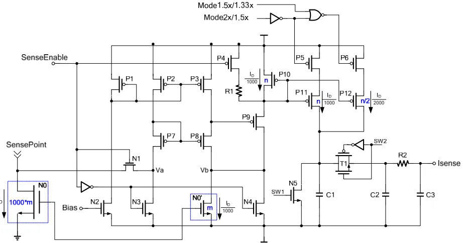
Fig.3.8 Hybrid Regulation Scheme for Improving Light Load Efficiency
Fig.3.8 shows the designed control diagram. Output voltage is regulated using a PID
compensator. Compensator output Vc is also used as the gate voltage of current source MN1,
so it is proportional to the current flowing through MN1 when it is on. ‘Ref1’ and ‘Ref2’ are
two references for deciding the load condition. Fixed-off-time generator controls the shut
down time in pulse skipping mode using the capacitor-charging circuitry. Voltage detector
all the light load control. Light-load control signal generator is responsible for generating the
PSM enable (PSM_ENB) and segmentation enable (SEG_ENB) signals based on the circuit
condition. Modes decision and driving sequence generator will output the driving signals for
ten transistors according to the Vin, PSM_ENB, and SEG_ENB.
The primary nodes waveforms are shown in Fig.3.9. During start-up, Vout increases from
zero and driving pulses are continuous. Vc decreases when Vout reaches 5V. Load condition is
judged using the output signal from current sensor. At heavy load condition, Isense is higher
than Ref1. When Isense is lower than Ref1 but higher than Ref2, charge pump operates in light
load condition. Device segmentation is enabled but the driving frequency is still 1MHz.
Ripple is smaller than that in heaving load. When Isense drops below Ref2, charge pump enters
very light load condition. The controller will be shut down for a fixed off time and then
restart. Eq. (3.27) gives the equation of off time. During the off time, load current is only
provided by discharging the output capacitor, and the output voltage drop can be derived
using (3.28). Therefore, smaller load current results in less voltage ripple.
C onstant
C ref o ff
C h a rg e
C V t
I
= = (3.27)
V-
out off outI
t
C
Δ
=
(3.28)When the controller is shut down, it is still able to respond to a load transient quickly using
the voltage detector. Since the decreasing slope of output voltage is proportional to the load
current during the off time, the output voltage should drop more sharply and results in more
voltage drop if a load step up happens. Without waiting for the end of the off time, the
controller will wake up once the output voltage touches the threshold. The primary
![Table 1.1 Commercial Charge Pump Products [15]](https://thumb-us.123doks.com/thumbv2/123dok_us/1489853.1182290/18.612.100.517.445.654/table-commercial-charge-pump-products.webp)