International Journal of Research
Available at https://edupediapublications.org/journalsp-ISSN: 2348-6848 e-ISSN: 2348-795X Volume 03 Issue 13 September 2016
Available online: http://internationaljournalofresearch.org/ P a g e | 494
Design & Simulation of 3-Phase 3-Level Voltage
Source Inverter for PV Synchronization to Grid
Y
adam.
N
agendra
1,
N
aresh.
B
andi
2& Veeranjaneyulu.Methra
31
Assistant Professor, Department of Electrical & Electronics Engineering, Narsimha Reddy
Engineering College, Maisammaguda; Rangareddy (Dt); Telangana, India.
2
Assistant Professor, Department of Electrical & Electronics Engineering, Narsimha Reddy
Engineering College, Maisammaguda: Rangareddy (Dt); Telangana, India.
3
M-tech Student Scholar, Department of Electrical & Electronics Engineering, Narsimha
Reddy Engineering College, Maisammguda; RangaReddy (Dt), TG, India.
Abstract: The Solar Photovoltaic (SPV) systems
which directly supply power to the grid are becoming more widely used. The photovoltaic (PV) field has given rise to a global industry capable of producing many gig watts (GW).The active and reactive power feed-in by grid-connected solar PV systems will result in voltage rise over its maximum limit in distribution systems. In This Project proposes different voltage control strategies to limit the voltage rise in low voltage distribution systems causedby grid connected solar P V systems. The voltage control strategies include four different active and reactive power control strategies. A power electronic converter which converts DC power from the PV array to AC power at required voltage and frequency levels is known as Inverter. Generally different Pulse Width Modulation (PWM) techniques have been implemented for grid connected 3-phase Voltage Source Inverter (VSI) system .On the basis of discussion of harmonic injection SPWM (HI-SPWM) and voltage space
vector PWM (VSV-PWM), a
novel SPWM technique (IF-SPWM), which is really simplest and well designed to obtain maximum inverter gain, minimum switching frequency and to avoid the disadvantages of HI-SPWM, is proposed. The IF-SPWM is based on instantaneously floating the equivalent neutral point of the output of a 3-phase inverter i.e. instantaneously injecting the same voltage waveform into the phase voltages. Modeling of photovoltaic systems includes modeling of SPV array, power electronics inverter/converter based on. In extension the proposed concept can be implemented for 3-phase 3-level VSI using SPWM for grid connected PV applications by using MATLAB/SIMULATION software
.Keywords: pulse width modulation; solar
photovoltaic; voltage source inverter.
1. Introduction
With exhaustion of natural resources and accelerated demand of conventional energy, the
problems of energy shortage and environmental pollution in the world have become of much importance that forced the planners and policy makers to look for alternative resources. The deregulation of electricity markets and requirement to reduce greenhouse gas emission from the conventional electric power generation make the distributed generation (DG) renewable energy systems gain a great opportunity as a new means of power generation that meet the accelerated demand for electric energy[1, 2].
Among all the various DG technologies, solar photovoltaic systems are rapidly growing in electricity markets due to the declining cost of PV modules, increasing efficiency of PV cells, manufacturing- technology enhancements and economics of scale [2, 3]. However, the increasing penetration levels of PV systems into the grid have given rise to potential problems relating to power quality (i.e. low power factor, harmonic distortion, etc.).
Fig. 1. General diagram of proposed system.
2. grid connected solar pv system
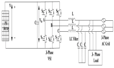
The general grid connected SPV system is shown in Fig.2. First stage PV array or module is connected with the system which connects the input to the inverter. The 3-phase VSI is used to convert DC voltage to AC voltage and feeds the energy to the load and grid [2] through LC filter circuit. The inverter has to be controlled in order to obtain harmonic less voltage to achieve good power quality. Various PWM techniques are used to switch the inverter circuit. A PLL is used for proper synchronization
Fig.2. General Block Diagram of Grid Connected SPV system.
A. Modeling of Solar PV
The Solar-PV cells are used to produce electricity by directly converting solar energy to electrical energy. Each solar cell is basically a p-n diode. As sunlight strikes a solar cell, the incident energy is converted directly into electrical energy without any mechanical effort. The voltage and current levels are produced from PV cells are very less, thus these PV cells are connected in series and parallel called modules and arrays to produce required voltage and current levels. The solar PV array is modeled by considering the output characteristics of PV panel which directly have relation with power converters which exists in the system. The solar PV cell is a non linear device which can be represented by a current source connected parallel with diode as shown in Fig.2. The characteristics of equivalent solar cell circuit are given
in (1).
(1) Where Ipv is the PV array output current, Vpv is the PV array output voltage, Ip his module photo current, R s is the series resistance, k is the Boltzmann constant (138e-23 J/K), A is the ideal factor, N sis the series no of cells and Np is parallel number of cells. T is the operating temperature [2]. The equation (1) is simulated using MATLAB/Simulink and P-V and I-V characteristics
are obtained. The operating curves shows that solar PV output power is function of solar irradiation.
Fig.3. PV Module.
B. 3-Phase VSI and Filter
A 3-phase VSI is used to convert DC voltage into AC voltage and feeds power to consumer loads and utility grid. The 3-phase inverters are used in grid connected SPV systems. A 3-phase inverter is a six step bridge inverter. It uses aminimum of six devices. As stated earlier, the transistor family of devices is now very widely used in inverter circuits. Presently the use of IGBT in three-phase inverter is on the rise. A capacitor connected at the input terminals tends to make the the input dc voltage constant. This capacitor also suppresses the harmonics fed back to the source. In inverter terminology, a step is defined as a change in the firing from one IGBT to the next IGBT in proper sequence. For one cycle of 360, each step would be of 60 intervals for a six step inverter. This means that the IGBT would be gated at regular intervals of a six step inverter. There are two possible patterns of gating the switches. In one pattern, each switch conducts for 180 and in the other each switches conducts for 120. But in both these patterns gating signals are applied and removed at 60 intervals of the output voltage [3]. A LC type filter is used to provide 50Hz frequency output to consumer loads and electric grid. There are various factors which decide the selection of filter capacitor and inductor. Generally in order to eliminate the higher order harmonics, the resonant frequency of the filter should be greater than 6 times of desired output frequency [4].
3. mathematical model of lc filter
The mathematical model of LC filter circuit has been derived using state space analysis [5]. LC output filter circuit for voltage and current equations is shown in Fig.4. Kirchhoff’s current law is applied to the nodes a, b, c shown in Fig.4.
International Journal of Research
Available at https://edupediapublications.org/journalsp-ISSN: 2348-6848 e-ISSN: 2348-795X Volume 03 Issue 13 September 2016
Available online: http://internationaljournalofresearch.org/ P a g e | 496
At node a,
(2) At node b,
(3) At node c,
(4) To make state equations, Kirchhoff’s voltage law is applied to inverter side and load side and finally state space equation for LC filter circuit is given in (5).
(5)
(6)
4. PWM techniques for 3-phase VSI
This section describes two types of PWM techniques used to control the 3-phase VSI of a grid connected SPV system.
A. Sinusoidal PWM (SPWM)
The SPWM technique is very simple and very easy to implement. This method produces a sinusoidal waveform by filtering an output pulse waveform by varying width. The required output voltage is achieved by varying the amplitude and frequency of modulating voltage. The pulse width can be changed by changing the amplitude and frequency of reference or modulating voltage. In Fig.5, modulating wave is compared with high frequency triangular wave from. The high switching frequency leads better output sinusoidal wave from. The switching state is changed when sine waveform is intersects with high frequency triangular waveform.
Fig.5. SPWM Control signal Generation.
In 3-phase VSI, the SPWM is achieved by three sinusoidal voltages (Va, Vb, Vc) which are 120 • out of phase with each other are compared with high
frequency triangular waveform(VT), and relative levels of the waveforms are used to control the switching the devices in each phase leg of the inverter.
Fig.6. SPWM Inverter.
3-phase VSI having six switches (S1-S6) with each phase output is connected to middle of the each inverter leg is shown in Fig.6. The output of the comparator forms the control signal for each leg of the inverter. In one lag, two switches makes a phase and these two switches open and close in a complementary fashion. The total voltage is Vdc, therefore the each pole voltage Vao, Vbo,Vco of the inverter varies between –Vdc/2and +Vdc/2. If the sine wave is greater than triangular wave, then upper switch is getting turned ON and lower switch is turned OFF. Based on switching states, positive or negative half DC link voltage is applied to each phase. Usually the switches are controlled in pairs (S1,S4),(S3,S6) and (S5,S2) and the logic is shown in Table I.
TABLE.I SWITCHING STATES
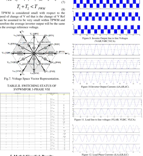
B. Space Vector Pulse Width Modulation
(SVPWM)
phase inverter corresponding to 8 voltage space vectors as shown in Table
C. The eight vectors, called the basic
space vectors include
Two zero vectors V0and V7and six non-zero V1-V6vectors. Two zero vectors have zero magnitude and six non-zero vectors have the same amplitude as shown in Figure 7. The angle between any adjacent two non-zero vectors is 60 degrees. • The desired reference voltage vector V ref given by the current controller can be approximated by using two adjacent vectors Vx, Vx+1(x=1,2,3,4,5,6) and zerovectors V0or V7for every PWM and the period TPWM is given in equation (6)
(7)
(8) • TPWM is considered small with respect to the speed of change of V ref that is the change of V Ref can be assumed to be very small within TPWM and therefore the average inverter output will be the same as the average reference voltage.
Fig.7. Voltage Space Vector Representation.
TABLE.II. SWITCHING STATUS OF SVPWMFOR 3-PHASE VSI
5. Matlab/Simulink Results
Figure 8. Matlab/Simulink Circuit diagram Grid Connected SPV system.
Figure.9. Inverter Output line to line Voltages (ViAB,ViBC,ViCA).
Figure 10.Inverter Output Currents (iiA,iiB,iiC).
Figure 11. Load line to line voltages (VLAB, VLBC, VLCA).
International Journal of Research
Available at https://edupediapublications.org/journalsp-ISSN: 2348-6848 e-ISSN: 2348-795X Volume 03 Issue 13 September 2016
Available online: http://internationaljournalofresearch.org/ P a g e | 498
Fig.13. Inverter output line voltage, Inverter output current, Load line
voltage, Load phase currents.
Inverter output line to line voltages are given in Fig. 9.The voltages are called as ViAB, ViBC, ViCA. Fig. 10 showsinverter output currents iiA, iiB, iiC. Load line to line voltagesand load phase currents iLA, iLB, iLC are given in Fig. 11 andFig 12. Inverter output line to line voltages (ViAB), Inverteroutput currents (iiABC), load line to line voltages (VLABC) andload phase currents (iLABC) are given in Fig.13.
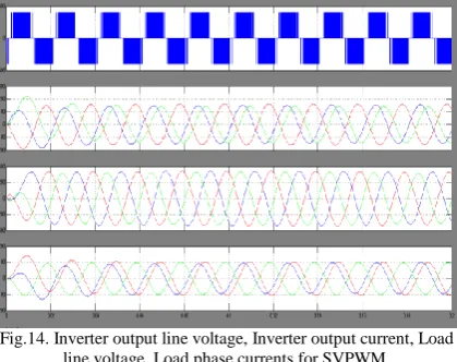
Fig.14. Inverter output line voltage, Inverter output current, Load line voltage, Load phase currents for SVPWM. Inverter output line to line voltages (ViAB), Inverteroutput currents (iiABC), load line to line voltages (VLABC) andload phase currents (iLABC) are given in Fig.14.
Fig.15.FFT analysis for Currents with SVPWM.
6. CONCLUSION
Increasing demand on energy efficiency and power quality issues, grid connected solar PV systems is taking a good place. In this paper SPWM and SVPWM techniques have been discussed for 3-phase grid connected VSI. The LC filter circuit is used in the proposed system. This filter circuit is mathematically modeled by using state space analysis and complete state space equation is obtained. The SPWM technique is implemented and simulated on 3 phases VSI using state space model of the LC filter circuit for grid connected solar PV system.Simulation mode of the current source inverter using the space vector pulse width modulation for producing thegate signals.The results clearly show the output has very less THD and produces much lower switching losses.
REFERENCES
[1] J.Y. Lee, and Y.Y. Sun, “A New SPWM Inverter with Minimum Filter Requirement,” International Journal of Electronics, Vol. 64, No. 5, pp. 815-826, 1988.
[2] K. Zhou and D. Wang, “Relationship Between Space-Vector Modulation and Three- Phase Carrier-Based PWM: A Comprehensive Analysis,” IEEE Transactions on Industrial Electronics, Vol. 49, No. 1, pp. 186- 196, February 2002.
[3] A.W. Leedy, and R.M. Nelms, “Harmonic Analysis of a Space Vector PWM Inverter using the Method of Multiple Pulses,” IEEE Transactions on Industrial Electronics, Vol. 4, pp. 1182-1187, July 2006.
[4] A.M. Khambadkone, and J. Holtz, “Current Control in Over-modulation Range for Space Vector Modulation based Vector Controlled Induction Motor Drives,” IEEE Industrial Electronics Society, Vol.2, pp. 1134- 1339, 2000.
[5] E. Hendawi, F. Khater, and A. Shaltout, “Analysis, Simulation and Implementation of Space Vector Pulse Width Modulation Inverter,” International Conference on Application of Electrical Engineering, pp. 124-131, 2010.
[6] H. Patangia and D. Gregory, “A Harmonic Reduction Scheme in SPWM,” IEEE Asia Pacific Conference on Circuits and Systems, pp. 1737-1740, 2006.
[7] A. Cataliotti, F. Genduso, A. Raciti, and G.R. Galluzzo, “Generalized PWM–VSI control algorithm based on a universal duty-cycle expression: Theoretical analysis, simulation results, and experimental validations,” IEEE Trans. Ind. Electron., vol. 54, pp. 1569 2007.
[8] V. Blasko, “Analysis of a hybrid PWM based on modified space-vector and triangle-comparison methods", IEEE Trans. Ind. Applicat., vol. 33, pp. 756 1997.
three-phase voltage source inverters,‟‟ IEEE Trans. Power Electron., vol. 24, no. 1, pp. 241–252, Jan. 2009. [10] C. Mei, J.C. Balda, and W.P. Waite, “Cancellation of common-mode voltages for induction motor drives using active method,” IEEE Trans. on Energy Conversion, vol. 21, no 2, pp. 380 – 386. June 2006.
[11] S. Ogasawara, H. Ayano, and H. Akagi, “An active circuit for cancellation of common-mode voltage generated by a PWM inverter,” IEEE Trans. on Power Electron., vol 13, pp. 835-841, September 1998.
Mr. YADAM NAGENDRA
received B.Tech degree from Kandula Obul Reddy memorial College of Engineering (JNTUA) in the year 2012 and received M.Tech in the stream of Power Electronics at St.Martin’s Engineering college (JNTUH) in the year 2014. Currently working as a Assistant Professor in Narsimha Reddy Engineering college for two years. His current research interests include power electronics for photovoltaic (PV) applications and PV generation and monitoring, include multilevel converters, power converters for distributed energy resources.
Mr.NARESH BANDI received B.Tech degree from ramappa Engineering college (JNTUH) in the year 2006 and received M.Tech in the stream of Power Electronics at P.indhra reddy memorial college of Engineering (JNTUH) in the year 2013. Currently working as a Assistant Professor in Narsimha Reddy Engineering College for one year. And his areas of interest are Applications of Power electronics in “Power Systems& Electrical machines”