Available online: https://edupediapublications.org/journals/index.php/IJR/ P a g e | 649
High-Speed Adder Energy-Efficient Carry Skip Adder Operating
Under a Wide Range of Supply Voltage Levels
V. Bhanu Preeti & T. Malleswarao
1M.tech-Scholar, Dept of ECE, Amalapuram Institute of Management Sciences and college of
Engineering, Mummidivaram, A.P.
2Assistant Professor, Dept of ECE, Amalapuram Institute of Management Sciences and college of
Engineering, Mummidivaram, A.P
Abstract: In this paper discussed about a carry skip adder (CSKA) structure with higher speed yet lower energy consumption compared with the
conventional adder. In moreover, utilize
multiplexer logic, the proposed structure make using NAND-NOR-Invert (NNI) and NOR-NAND-Invert (NNI) compound gates for the skip logic. The structure may be realized with both fixed and variable stage size styles, further improves the energy and speed parameters of the adder. Finally, a hybrid variable proposed adder structure, which lowers the power consumption affect the speed, is presented. The proposed architecture of this paper analysis the logic size, area and power consumption using Xilinx.
KEYWORDS: Carry skip adder (CSKA),energy efficient, high performance, hybrid variable latency adders, voltage scaling
I. INTRODUCTION
There are many works on the subject of optimizing the speed and power of these
units, which have been reported.
Obviously, it is highly desirable to achieve higher speeds at low-power / energy consumptions, which is a challenge for the designers of general purpose processors. One of the effective techniques to lower the power consumption of digital circuits is to reduce the supply voltage due to quadratic dependence of the switching energy on the voltage. Moreover, the sub threshold current, which is the main leakage component tin OFF devices, has an exponential dependence on the supply voltage level through the drain-induced barrier lowering effect. Depending on the amount of the supply voltage reduction,
the operation of ON devices may reside in the super threshold, near-threshold, or sub threshold regions. Working in the super threshold region provides us with lower delay and higher switching and leakage powers compared with the near/sub threshold regions. In the sub threshold region, the logic gate delay and leakage power exhibit exponential dependences on
the supply and threshold voltages.
Moreover, these voltages are
(potentially)subject to process and
environmental variations in the nano scale technologies. The variations increase uncertainties in the a fore said performance parameters .In addition, the small sub threshold
current causes a large delay for the circuits operating in the sub threshold region.
Available online: https://edupediapublications.org/journals/index.php/IJR/ P a g e | 650
of the power (and performance) on the supply voltage has been the motivation for design of circuits with the feature of dynamic voltage and frequency scaling. In these circuits, to reduce the energy consumption, the system may change the voltage (and frequency)of the circuit based on the work load requirement.
For these systems, the circuit should be able to operate under a wide range of supply voltage levels. Of course, achieving higher speeds at lower supply voltages for the computational blocks, with the adder as one the main components, could be crucial in the design of high-speed, yet energy efficient, processors. In addition to the knob of the supply voltage, one may
choose between different adder
structures/families for optimizing power and speed. There are many adder families with different delays, power consumption. Conventional carry skip adder:
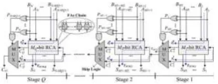
The structure of an N-bit Conv-CSKA, is based on blocks of the RCA (RCA blocks), is shown in Fig. 1. In addition to the chain of FAs in each stage, there is carry skip logic. For an RCA that contains N cascaded FAs, the worst propagation delay of the summation of two N-bit numbers, A and B, belongs to the case where all the FAs are in the propagation mode.
Figure 1: Conventional structure of the CSKA
This shows that the delay of the RCA is linearly related to N. In the case, where a group of cascaded FAs are in the propagate mode, the carry output of the chain is equal to the carry input. In the CSKA, the carry skip logic detects this situation, and makes the carry ready for the next stage without waiting for the operation of the FA chain to be completed. The skip operation is performed using the gates and the multiplexer shown in the figure. Based on this explanation, the NFAs of the CSKA are grouped in Q stages. Each stage contains an RCA block with Mj FAs (j =1... Q) And skip logic. In each stage, the inputs of the multiplexer (skip logic) are the carry input of the stage and the carry output of its RCA block (FA chain). In addition, the product of the propagation signals (P) of the stage is used as the selector signal of the multiplexer.
III. EXISTED SYSTEM
In the existed hybrid structure, the prefix network of the Brent–Kung adder is used for constructing the nucleus stage. One the advantages of the this adder compared with other prefix adders is that in this structure, using forward paths, the longest carry is calculated sooner compared with the intermediate carries, which are computed by backward paths.
In addition, the fan-out of adder is less than other parallel adders, while the length of its wiring is smaller. Finally, it has a simple and regular layout. The internal
structure of the stage p, including the
modified PPA and skip logic, is shown in Fig. 2. Note that, for this figure, the size of
Available online: https://edupediapublications.org/journals/index.php/IJR/ P a g e | 651
Fig.2. Internal structure of the pth stage of the existed hybrid variable latency CSKA.
As shown in the figure, in the
preprocessing level, the propagate signals (Pi ) and generate signals (Gi ) for the inputs are calculated. In the next level, using Brent–Kung parallel prefix network, the longest carry (i.e., G8:1) of the prefix
network along with P8:1, which is the
product of the all propagate signals of the inputs, are calculated sooner than other intermediate signals in this network. The
signal P8:1 is used in the skip logic to
determine if the carry output of the
previous stage (i.e., CO,p−1) should be
skipped or not.
In addition, this signal is exploited as the predictor signal in the variable latency adder. It should be mentioned that all of these operations are performed in parallel
with other stages. In the case, where P8:1
is one, CO,p−1 should skip this stage
predicting that some critical paths are
activated. On the other hand, when P8:1 is
zero, CO,p is equal to the G8:1.
In addition, no critical path will be activated in this case. After the parallel prefix network, the intermediate carries,
which are functions of CO,p−1 and
intermediate signals, are computed.
Finally, in the post processing level, the output sums of this stage are calculated. It should be noted that this implementation is based on the similar ideas of the concatenation and incrementation concepts used in the CI-CSKA. It should be noted that the end part of the SPL1 path from
CO,p−1 to final summation results of the
PPA block and the beginning part of the SPL2 paths from inputs of this block to
CO,p belong to the PPA block. In addition, similar to the existed CI-CSKA structure, the first point of SPL1 is the first input bit of the first stage, and the last point of SPL2 is the last bit of the sum output of
the incrementation block of the stage Q.
The steps for determining the sizes of the stages in the hybrid variable latency CSKA structure are similar. Since the PPA structure is more efficient when its size is equal to an integer power of two, we can select a larger size for the nucleus stage accordingly.
This implies that the third step discussed is modified. The larger size (number of bits), compared with that of the nucleus stage in the original CI-CSKA structure, leads to the decrease in the number of stages as well smaller delays for SLP1 and SLP2. Thus, the slack time increases further.
Available online: https://edupediapublications.org/journals/index.php/IJR/ P a g e | 652
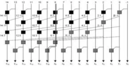
The Han-Carlson prefix tree is similar to the Kogge-Stone's structure since it has a maximum fan-out of 2 or f = 0. The difference is that Han-Carlson prefix tree utilizes much less cells and wire tracks than Kogge-Stone. The cost is one extra logic level. Han-Carlson prefix tree can be viewed as a sparse version of Kogge-Stone prefix tree. The fan-out at all logic levels is the same. In Kogge-Stone's structure the pseudo-code can be easily modified to build a Han-Carlson prefix tree. The major difference is that in each logic level, Han-Carlson prefix tree places cells every other bit and the last logic level accounts for the missing carries.
Fig 2. 16-bit Han-Carlson prefix Tree
A16-bit Han-Carlson prefix tree is shown in above figure, ignoring the buffers. The critical path is shown with thick solid line. Han-Carlson adder provides a good trade-off among fanout, number of logic levels and number of black cells. In Han-Carlson topology, the outer rows are represented as Brent-Kung graphs, while the inner rows are represented as Kogge-Stone graphs.
Fig 3. 16-bit Han- Carlson topology
Fig 3 shows the Han-Carlson adder which utilizes a single Brent-Kung level at the beginning and at the end of the graph, the
number of levels is 1+ 𝑙𝑜𝑔2(𝑛). Here black
dots represent the prefix operator, while white dots are represented as simple placeholders.
Han-Carlson adder constitutes a good trade-off between fanout, number of logic levels and number of black cells. Due to this, Han-Carlson adder can achieve equal speed performance with respect to Kogge-Stone adder, at lower power consumption and area. Hence, it is interesting to implement a speculative Han Carlson adder. Due to these reasons, we have generated a Han-Carlson speculative prefix-processing stage by deleting the last rows of the Kogge-Stone part of the adder.
Available online: https://edupediapublications.org/journals/index.php/IJR/ P a g e | 653
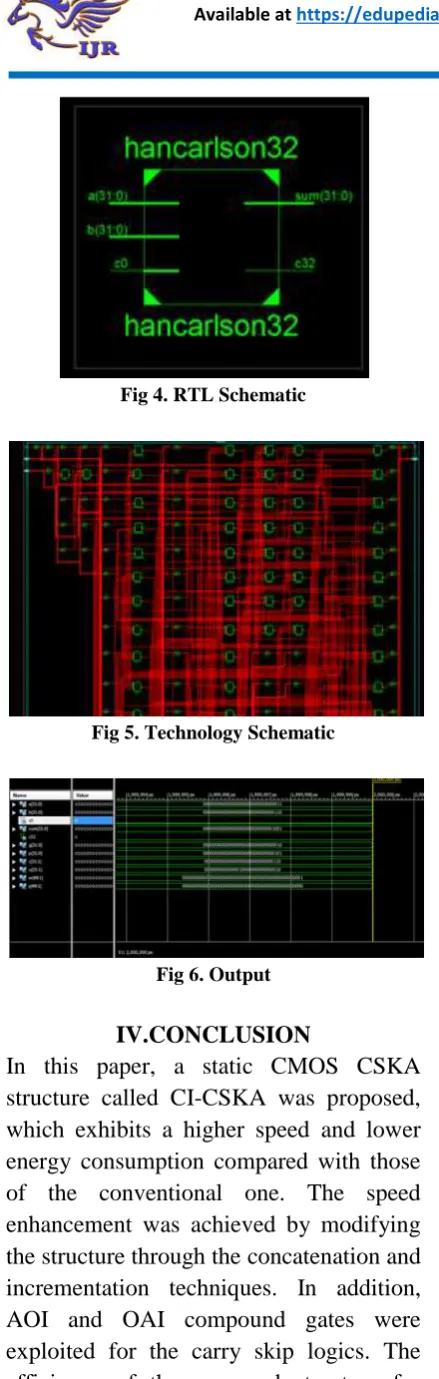
Fig 4. RTL Schematic
Fig 5. Technology Schematic
Fig 6. Output
IV.CONCLUSION
In this paper, a static CMOS CSKA structure called CI-CSKA was proposed, which exhibits a higher speed and lower energy consumption compared with those of the conventional one. The speed enhancement was achieved by modifying the structure through the concatenation and incrementation techniques. In addition, AOI and OAI compound gates were exploited for the carry skip logics. The efficiency of the proposed structure for both FSS and VSS was studied by
comparing its power and delay with those of the Conv-CSKA, RCA, CIA, SQRT-CSLA, and KSA structures. The results revealed considerably lower PDP for the VSS implementation of the CICSKA structure over a wide range of voltage from super-threshold to near threshold.
The results also suggested the CI-CSKA structure as a very good adder for the applications where both the speed and energy consumption are critical. In
addition, a hybrid variable latency
extension of the structure was proposed. It exploited a modified parallel adder structure at the middle stage for increasing the slack time, which provided us with the opportunity for lowering the energy consumption by reducing the supply voltage.
V. REFERENCES
[1]. A. Tyagi, “A reduced area scheme for carry-select adders”, IEEE Trans. on Computer, vol. 42, pp. 1163- 1170, 1993 [2]. Hasan Krad and Aws Yousif Al-Taie, “Performance Analysis of a 32-Bit Multiplier with a Carry-Look-Ahead Adder and a 32-bit Multiplier with a Ripple Adder using VHDL”, Journal of Computer Science 4 (4): 305-308, 2008. [3]. Sauvagya Ranjan Sahoo, Kamala Kanta Mahapatra, "Design of Low Power and High Speed Ripple Carry Adder Using Modified Feed through Logic" in 2012
International Conference on
Available online: https://edupediapublications.org/journals/index.php/IJR/ P a g e | 654
[5]. A Koren, Computer Arithmetic Algorithms, 2nd ed. Natick, MA, USA: A K Peters, Ltd., 2002.
[6]. R. Zlatanovici, S. Kao, and B. Nikolic, “Energy–delay optimization of 64-bit carry-look ahead adders with a 240ps 90 nm CMOS design example,” IEEE J. Solid-State Circuits, vol. 44, no. 2, pp. 569–583, Feb. 2009.
[7]. S. K. Mathew, M. A. Anders, B.
Bloechel, T. Nguyen, R. K.