warwick.ac.uk/lib-publications
Original citation:
Burrows, Christopher W., Hase, Thomas P. A., Ashwin, M. J., Mousley, P. and Bell, Gavin R..
(2016) Depth sensitive X-ray diffraction as a probe of buried half-metallic inclusions. Physica
Status Solidi. B: Basic Research. doi: 10.1002/pssb.201600543
Permanent WRAP URL:
http://wrap.warwick.ac.uk/85857
Copyright and reuse:
The Warwick Research Archive Portal (WRAP) makes this work of researchers of the
University of Warwick available open access under the following conditions.
This article is made available under the Creative Commons Attribution 4.0 International
license (CC BY 4.0) and may be reused according to the conditions of the license. For more
details see: http://creativecommons.org/licenses/by/4.0/
A note on versions:
The version presented in WRAP is the published version, or, version of record, and may be
cited as it appears here.
as a probe of buried half-metallic
inclusions
C. W. Burrows, T. P. A. Hase, M. J. Ashwin, P. J. Mousley,and G. R. Bell*
Department of Physics, University of Warwick, Coventry CV4 7AL, UK
Received 14 August 2016, revised 4 October 2016, accepted 5 October 2016 Published online 31 October 2016
Keywords epitaxy, half-metals, spintronics, X-ray diffraction
∗Corresponding author: e-mail[email protected], Phone:+44-24-76523489, Fax:+44-24-76150897
This is an open access article under the terms of the Creative Commons Attribution License, which permits use, distribution and reproduction in any medium, provided the original work is properly cited.
The ferromagnetic material MnSb can exist in two polymorphs in epitaxial thin-film form, namely niccolite n-MnSb and cubic c-MnSb. We investigate the behavior of these polymorphs using grazing incidence depth-dependent in-plane X-ray diffraction.
The in-plane lattice parameter evolution of a nominal 3000 ˚A
thin film reveals a small near-surface compression of∼0.1% in
the majority n-MnSb component. A similar effect is also ob-served for the cubic polymorph, suggesting that the local strain environment of these crystallites is dominated by the n-MnSb
matrix. Collated in-plane X-ray diffraction data from a GaAs/
In0.5Ga0.5As(111)/MnSb heterostructure in the near-surface
re-gion with probing depths ranging between 20 and 450 ˚A. Present
are two of the polymorphs of MnSb: the niccolite (n-) and cubic zincblende (c-) phases.
1 Introduction Half-metallic ferromagnetic (HMF) materials have high potential in hybrid semiconductor spin-tronic devices, especially if they can be grown in thin films. Molecular beam epitaxy (MBE) has been used to grow a variety of thin-film HMF materials including semi-Heusler alloys [1, 2], full-Heusler alloys [3–5], and binary transition-metal pnictides including MnSb [6–10]. Of the HMF family of materials, the binary transition-metal pnictides, in particu-lar those containing Mn, are especially attractive candidates for thin film spintronic applications due to their epitaxial and chemical compatibility with a range of semiconducting sub-strates. The Mn pnictides are not HMF materials in their usual niccolite hexagonal (n-) polymorph. However, zincblende cubic (c-) polymorphs of MnBi [11], MnSb [12], and MnAs [13] are predicted to be HMF materials. Furthermore, ac-cording to extended density functional theory calculations incorporating finite temperature effects through the
disor-dered local moments approach, c-MnSb promises a wide minority spin gap and robust 100% spin polarization even at room temperature [12].
phy s i c a
s
s
p
status
s
oli
d
i b
2 C. W. Burrows et al.: Depth sensitive XRD as probe of buried inclusions
The bulk structure of n-MnSb is the double hexag-onal close packed B81 structure with lattice parameters
a=4.128 ˚A andc=5.789 ˚A [21]. Conversely, c-MnSb has the cubic B3 zincblende structure and we have observed lat-tice parameters b of between 6.435 and 6.502 ˚A [12, 20] (in this paper, cubic materials are assigned lattice parame-tersbi). The somewhat large range of observed cubic lattice
parameters is due to their strong correlation with inclusion crystallite size. The epitaxial mismatch between the majority n-MnSb layer and the In0.5Ga0.5As(111)A virtual substrate is
only∼0.31%. However, a far larger mismatch of 10.1% ex-ists between the n-MnSb matrix and the c-MnSb polymorph embedded within it. It is this very high mismatch which causes the variation in c-MnSb lattice parameter with crys-tallite size.
In the present paper, we make use of the high fluxes and increased angular resolution available at synchrotron ra-diation sources to explore the depth-dependent behavior of MnSb epilayers grown on In0.5Ga0.5As(111)A substrates. We
use grazing incidence in-plane X-ray diffraction (GIXRD) to determine the crystallographic behavior of the near-surface region of a nominally 3000 ˚A thick MnSb(0001) film.
2 Experimental details A 3000 ˚A thick MnSb epi-layer was grown on an In0.5Ga0.5As(111)A virtual substrate
by MBE using optimized growth conditions [20]. The sample was not capped with Sb, which we typically use to passivate the surface and prevent oxidation [22], in order to avoid confusion between diffraction features arising from the cubic polymorph and elemental Sb.
High-resolution XRD experiments were performed us-ing 10 keV photons at the ESRF synchrotron (France) on the XMaS beamline. The diffractometer was operated in a six-circle configuration and the experiments were performed at atmospheric pressure with the sample under flowing nitro-gen. The sample rested on two additional perpendicular arcs of rotation to ensure that the surface was flat with respect to the incident X-ray beam within an error of less than 0.05◦. For the symmetric out-of-plane experiments (whereQis aligned parallel to the surface normal), the system was operated in a pseudo four-circle mode with standard coupledθV-2θVscans
performed alongside asymmetric reciprocal space maps. Fur-ther details are given in Ref. [20]. For the in-plane symmet-ric scans (whereQis perpendicular to the surface normal), a series of azimuthal sample rotations coupled with in-plane arm movementθH–2θHwas used as a function of sample
az-imuth. A schematic of the diffraction geometry used is given in Fig. 1. For depth dependence studies, a small incident angle
αi was induced by tilting the entire diffractometer about its
center of rotation. This ensured the incident angle remained fixed as a function of sample rotation. The optimizedαfwas
found by maximizing the scattered intensity by scanning 2θV.
3 Scattering geometry When the incidence angle of the primary X-ray beam is below the value for the critical an-gle then total external reflection occurs and only an evanes-cent wave penetrates into the sample surface. As a
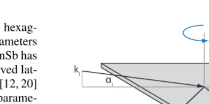
[image:3.728.317.524.94.197.2]conse-ki kf 2θ Q αi αf
Figure 1 Schematic of the in-plane diffraction geometry used,ki
andkfare the incident and final X-ray wave-vectors,Qis the
scat-tering vector, which is very nearly in-plane and features a smallQz
component.αiandαfare incident and final grazing angles.
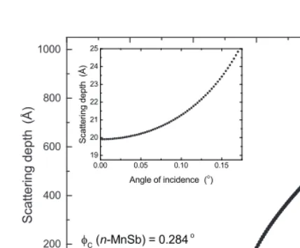
quence, the effective penetration depth of the X-ray beam drops dramatically, typically down to tens of ˚A. This results in a high level of surface specificity which can be controlled through adjustment of incident angle [23]. We note that an advantage of the in-plane geometry used here for depth-dependent studies is that refractive effects are minimized and soQremains unchanged, unlike other depth-sensitive scat-tering techniques such as parallel beam powder diffraction, to determine the effective scattering depth, defined as the depth at which the electric field has been reduced by a value of 1/e, as a function of incident angle we use the formalism devel-oped by Dosch et al. [24]. The scattering depthΛis given by
Λ= λ
2π(li+lf)
, (1)
whereliandlfare
li,f= √
2
2 {(2δ−sin
2α
i,f)2+[(sin2αi,f−2δ)2+(2β)2]
1 2}
1 2.
(2)
Here,δandβrelate to dispersion and absorption effects in the complex refractive index of the near surface region. The anglesαi,fare the angles of the primary (incident) and
scat-tered (final) X-ray beams with respect to the sample surface defined in Fig. 1. For MnSb at 10 keV, the values ofδandβ
are 1.227×10⁻⁵
and 9.47×10⁻⁷
, respectively. The variation in scattering depth calculated from Eq. (1) as a function of incident angle is shown in Fig. 2. Due to the presence of a non-stoichiometric surface oxide [25], the use of values forδ
andβderived for pure MnSb may introduce a small system-atic error on the calculated scattering depth. The penetration depth varies from approximately 20 ˚A at very low angles to
∼750 ˚A for an incident angle of 0.5◦. However, scattering will be measured from a depth up to three times greater than these values due to the slowly decaying amplitude of the elec-tric field into the sample. The dashed line in the main figure body highlights the position of the critical angle,αc, at 0.284◦
as calculated using the relationαc=λ·(re·ρe−/π)
1 2. Above this angle, total external reflection no longer occurs and the scattering volume increases rapidly. The inset in Fig. 2 shows the behavior of the scattering depth for incidence angles
Figure 2 The scattering depthΛcalculated for n-MnSb. The inset
shows low angles, well below the critical angleφcfor n-MnSb, at
an expanded scale.
between 0 and 0.17◦ showing the depth sensitivity of the technique at very grazing angles.
4 Results and discussion Figure 3 shows RHEED patterns obtained from the clean In0.5Ga0.5As(111)A virtual
substrate and the MnSb(0001) layer after growth. The pat-terns exhibit the expected (2× 2) reconstruction for both surfaces [8, 20]. The patterns confirm the in-plane epitaxial relation as GaAs[110] parallel to MnSb[2110] which is con-sistent with our growth on both GaAs and Ge substrates. The spacing of the RHEED streaks is consistent with an in-plane surface lattice parameter of a=4.14±0.05 ˚A, the value usually measured for relaxed MnSb(0001). Using conven-tional out-of-plane symmetric XRD, the lattice parameters of the In0.5Ga0.5As(111)A substrate and the n-MnSb film are
bsub = (5.853±0.001) ˚A andc= (5.768±0.001) ˚A,
respec-tively. On the basis of asymmetric reciprocal space mapping, the in-plane n-MnSb lattice parameter is (4.153±0.008) ˚A. The mosaic width of the virtual substrate (0.543◦) is deter-mined by the relatively large epitaxial mismatch between it and the GaAs substrate (∼3.7%), and this mosaicity in-fluences the crystal quality of the MnSb epilayer. Both XRD and electron microscopy have revealed crystalline inclusions of c-MnSb within the predominantly n-MnSb film [20]. The in-plane and out-of-plane lattice parameters of these cubic inclusions are (6.429±0.008) ˚A and (6.435±0.008) ˚A, re-spectively.
In-plane GIXRD data withQaligned along both prin-cipal in-plane directions were obtained using the geometry shown in Fig. 1 and all data sets were fitted carefully us-ing a reducedχ2
minimization routine. Peaks were fitted us-ing Pearson VII functions and backgrounds were fitted with either polynomials (longQrange scans) or tanh functions (shortQrange scans). Care was taken to avoid artefacts due to background choice. The uncertainties on fitting parame-ters were found by determining the extent of theχ2
= 1 contour [26].
(b) (a)
(d) (c)
In0.5
Ga
0.5
A
s
(111
)A
(2x2)
[image:4.728.308.544.93.276.2]MnSb(0001)-(2x2)
Figure 3 Typical RHEED patterns before and after MnSb growth
on the In0.5Ga0.5As(111)A virtual substrate.
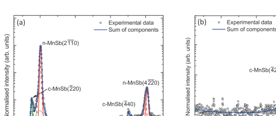
Typical in-plane GIXRD data obtained at an incidence angle of 0.5◦ (Λ= 750 ˚A) are shown in Fig. 4, with Q
aligned along the GaAs[110] and GaAs[211] directions along with total fits, peak components, and background (sixth or-der polynomial). Focusing on the GaAs[110] direction first, the expected n-MnSb{2110}and c-MnSb{220}reflections are present. To obtain a good fit, an additional but small peak was required. This additional scattering may either arise from diffuse scattering from defects or, more likely, from the In0.5Ga0.5As substrate. The substrate peak is
broad-ened as we are relatively far from the diffraction condi-tion, only measuring the tails of the (220) peak convolved with the crystal truncation rod. The asymmetric shape of the n-MnSb(4220) and c-MnSb(220) reflections suggest that they consist of two sets of reflections arising from crystallites with distinct lattice parameters. In fact, it was not possible to satisfactorily fit the data without two contributions for each of the four diffraction peaks. For c-MnSb, the dominant sub-peak in each pair (solid green lines) appears at lowerQ val-ues while for n-MnSb, the larger sub-peak appears at higher
Q values (solid red lines). The data with Q aligned along the GaAs[211] direction are somewhat simpler, with only two diffraction features present (Fig. 4b), These are indexed to the c-MnSb(422) and n-MnSb(3300). The fitting reveals that these sub-peaks correspond to n-MnSb lattice parame-ters ofa1=(4.152±0.001) ˚A anda2=(4.188±0.001) ˚A,
and c-MnSb parameters of b1= (6.429±0.001) ˚A and
b2=(6.347±0.004) ˚A (suffix 1 denotes the more intense
sub-peak in each case). Both in-plane parameters are consis-tent with the (less accurate) RHEED measurements.
phy
s
i
c
a
s
s
p
status
s
oli
d
i b
4 C. W. Burrows et al.: Depth sensitive XRD as probe of buried inclusions
[image:5.728.57.540.90.294.2](a)
(b)
Figure 4 In-plane GIXRD scans withQaligned along the (a) GaAs[110] direction and (b) GaAs[211] direction. Along both directions,
four diffraction peaks due to c-MnSb (green) and n-MnSb (red) are labeled, the solid lines indicate the most intense component. The gray
lines correspond to weak reflections from the In0.5Ga0.5As(111)A/GaAs(111)A virtual substrate.
were used, with a low intensity In0.5Ga0.5As(111)A
reflec-tion included at the expected (220) posireflec-tion. For scattering depths below 70 ˚A, the c-MnSbb2lattice parameter was
con-strained to values smaller than 6.350 ˚A. This was done such that the intensity of the second cubic component could be de-termined without introducing fitting artefacts whereby theb2
sub-peak would end up distorting to accommodate the tails of thea1sub-peak. As such, it should be noted that the area of
theb2peak as determined from fitting is only broadly
repre-sentative of the scattered intensity. Figure 5 shows a typical reducedQrange GIXRD scan, with best fit to the data, for an incidence angle of 0.375◦(Λ=450 ˚A). The inset of Fig. 5 shows a close-up of the n-MnSb(2110) reflections on a lin-ear vertical scale, highlighting the quality of the fit to the data.
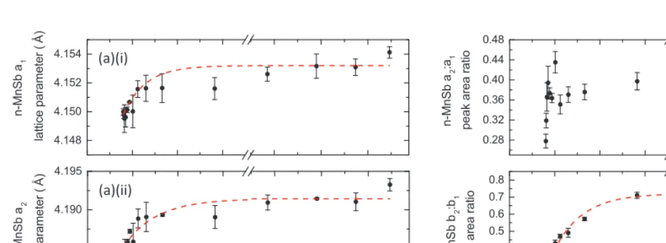
The evolution of the n-MnSb a1 anda2 lattice
param-eters is shown in Fig. 6a(i) and (ii). The n-MnSb a1
pa-rameter varies from (4.150±0.001) ˚A to (4.154±0.001) ˚A while thea2 parameter varies between (4.183±0.001) ˚A to
(4.193±0.001) ˚A for scattering depths of 20 and 450 ˚A. These represent−0.1% and−0.25% changes ina1anda2,
re-spectively, relative to the lattice parameters at highΛ. The c-MnSb lattice parameters (not shown) exhibit similar changes over the scattering depths probed although the b2
parame-ter settles at a constraint value below scatparame-tering depths of 70 ˚A. Theb1parameter changes from (6.417±0.001) ˚A in
the near surface region to (6.424±0.001) ˚A deeper into the film, a –0.1% shift. The red dashed lines in Fig. 6a(i) and (ii) are exponential functions fitted to the data to highlight the near-surface decay of the parameters. The decay constant for thea1parameter is (17±5) ˚A while fora2 it is (12±3) ˚A.
This suggests that the relaxation observed in the near-surface region extends over approximately 40 ˚A (including the
mini-mum 20 ˚A scattering depth arising from the evanescent wave present in the sample).
The lattice parameter of bulk single-crystal MnSb is
a=4.128 ˚A, smaller than the values ofa1anda2observed
here. It is possible that even strain-relaxed (0001) thin-film material still contains extended defects which increase the in-plane lattice parameter from the value for bulk material. A bimodal lattice parameter distribution could arise from the formation of anti-phase boundaries (APBs), which would
Figure 5 Typical GIXRD in-plane scan with corresponding best fit,
obtained with an incidence angle of 0.375◦(Λ=450 ˚A). Reflections
from c-MnSb (green), n-MnSb (red) and the In0.5Ga0.5As(111)A
substrate (gray) are present. The inset shows a zoom of the n-MnSb(2110) region on a linear scale.
[image:5.728.307.540.489.686.2](b)(ii) (a)(ii)
Figure 6 Evolution of the n-MnSb in-plane lattice parameters (a)(i)a1and (a)(ii)a2as a function of scattering depth. Change in peak
area ratio for the (b)(i) n-MnSb and (b)(ii) c-MnSb sub-peaks as a function of scattering depth. The dashed red lines correspond to fitted exponential decay functions, which also serve as a guide to the eye.
occur in this material system due to the difference in stack-ing orders within the film caused by terrace steps on the substrate. The In0.5Ga0.5As(111)A virtual substrate has
sur-face step heightsb/√3=3.38 ˚A, not far from the value of
c/2=2.89 ˚A for n-MnSb. The stacking of hexagonal close-packed planes in the n-MnSb B81 structure is ABAC, with
Mn on A sites and Sb on B and C sites. It is possible that n-MnSb APBs, extending throughout the film, arise due to regions with Mn–B–Mn–C stacking adjoining regions with Mn–C–Mn–B stacking. The steric effect among Sb atoms in adjoining regions would tend to increase the in-plane lattice parameter, but this effect would be much smaller out-of-plane due to the separation of Sb layers by the intervening layers of Mn. On this basis, regions with measured lattice parameter
a2 could be those including APBs, whilea1 is
representa-tive of APB-free n-MnSb, and thecparameter would not be expected to change significantly.
The near-surface relaxation observed could arise from several effects. Relatively thick Mn-rich native oxide layers can form on uncapped MnSb films which in extremis can extend to∼5 nm [25]. This amorphous oxide, which damps the electric field in the sample and thereby reducing the in-tensity of the observed diffraction peaks, could induce strain in the neighboring MnSb, although this effect is difficult to quantify given its non-stoichiometric composition and lack of long range crystalline order. Surface roughness and a locally variable oxide layer thickness could allow some in-plane re-laxation of the MnSb at the surface. It is also possible that oxide formation is enhanced along extended defects near the surface leading to relaxation of their associated strain. This is consistent with the increased relaxation observed in thea2
lattice parameter compared toa1, ifa2is attributed to
defec-tive n-MnSb.
Figure 6b(i) and (ii) show the ratio of the sub-peak areas for the n-MnSb and c-MnSb reflections, respectively. In the n-MnSba2toa1ratio [panel (b)(i)], there is an increase from
(0.278±0.014) to∼0.36 as the scattering depth decreases
although no clear trend is present since the ratio returns to
∼0.28 at small scattering depths. It can be seen that both defective and non-defective MnSb are present throughout the upper 450 ˚A of the film. This would be consistent with APBs which are not readily “healed” during epitaxy. It is known that threading dislocations with Burgers vector (c/2)[0001] penetrate to the surface of MnSb/GaAs(111) films [8], and localized misfit dislocation arrays have been observed at the interfaces [12, 20] but a more extensive study of extended defects would be required to understand in detail the behavior of this epitaxial system.
Figure 6b(ii) shows the ratio of the c-MnSbb2tob1peak
areas which reveals a much clearer trend. At higher scattering depths (Λ≥70 ˚A) both components are present with similar peak area. Toward the surface the proportion of theb2
com-ponent (b2 < b1) drops off significantly, with a similar decay
length to those observed for the lattice parameter changes. On the basis of the out-of-plane measurements presented in Ref. [20], the lowerQc-MnSb component is the more preva-lent in the layer with the smaller lattice parameter compo-nent existing deeper into the film. This is consistent with the present in-plane results. Even though the dominant c-MnSb component with largerb1 becomes more prevalent near the
surface, its own lattice parameter relaxes downward along with that of the surrounding n-MnSb matrix. This suggests that in-plane relaxation due to the proximity of the surface and native oxide is mediated to the c-MnSb inclusions via the n-MnSb matrix. The relaxation toward the surface ob-served in Fig. 6 is independent of any systematic error in the determination of the incident angle which would only cause a slight shift along the depth axis.
phy s i c a
s
s
p
status
s
oli
d
i b
6 C. W. Burrows et al.: Depth sensitive XRD as probe of buried inclusions
– RSMs). The limitedQresolution of the RSMs precludes a detailed determination of the lattice parameters from such data. From the RSM peak maxima, however, we can esti-mate the in-plane lattice parameters of the dominant phases. These are in excellent agreement with thea1andb1values
re-ported herein. Symmetric scans recorded along the n-MnSb [0001] direction with higher Q resolution showed a two-component peak at the c-MnSb(111) position (Figs. 3(b) and 4(b) of [20]). The lattice parameters of these components are in agreement with bothb1andb2, consistent with undistorted
cubic structures. Conversely, no such split into two compo-nents is observed at the n-MnSb(0002) peak position. This is consistent with the presence of APBs extending throughout the thickness of the film which affect theaparameter much more strongly than thecparameter.
5 Conclusion We have exploited the tunable depth sensitivity of GIXRD when performed on a six-circle diffrac-tometer to study in-plane diffraction from a MnSb (0001) thin film grown on an In0.5Ga0.5As(111)A virtual substrate.
The predominantly n-MnSb epilayer contains strained c-MnSb(111) crystallites which extend at least 400 ˚A into the film. For both polymorphs, the in-plane XRD must be fitted with two components of slightly different lattice parameters. For the n-MnSb polymorph, it is suggested that extended de-fects such as APBs are responsible for the component with larger lattice parameter. For c-MnSb, the stronger in-plane lattice parameter [(6.429±0.001) ˚A] is in excellent agree-ment with lattice parameters [(6.429±0.008) ˚A] for thin films on In0.5Ga0.5As(111)A measured previously by
recip-rocal space mapping [20]. All of the lattice parameters vary with depth, with both n-MnSb values relaxing to lower values within∼40 ˚A of the surface. The stronger c-MnSb peak fol-lows this relaxation while the weaker component at smaller lattice parameter drops in intensity toward the surface.
This work confirms that c-MnSb inclusions can be sta-bilized within n-MnSb epilayers and shows additionally that the strain state of the c-MnSb is linked to that of the surround-ing n-MnSb matrix. Our density functional theory (DFT) work suggests that over the range of strains observed in c-MnSb the material remains robustly HMF, important for its application in spintronics. Further, DFT work would be valu-able in assessing the local role of strain and extended defects such as APBs on the magnetic properties of both n-MnSb and c-MnSb.
The GIXRD method can provide detailed depth-resolved information on varying strain states within an epitaxial film as close as 20 ˚A to the surface without the need for ultra-high vacuum. Even for the low-strain films studied here, significant surface relaxation has been observed. We will discuss results on Sb-capped ultra-thin (10 ˚A to 50 ˚A) MnSb(0001)/GaAs(111) films in a future paper, where the in-plane strain due to epitaxial mismatch with the substrate is dominant.
Acknowledgements This work was supported by EPSRC
(UK) under grant numbers EP/K032852/1 and EP/K03278X/1.
XMaS is a mid-range facility funded by EPSRC. We are grate-ful to the beamline staff at XMaS and to R. Johnston at Warwick for their expert help and technical assistance.
References
[1] W. V. Roy, J. D. Boeck, B. Brijs, and G. Borghs, Appl. Phys. Lett. 77(25), 4190–4192 (2000).
[2] P. Bach, A. S. Bader, C. Ruster, C. Gould, C. R. Becker, G. Schmidt, L. W. Molenkamp, W. Weigand, C. Kumpf, E. Umbach, R. Urban, G. Woltersdorf, and B. Heinrich, Appl.
Phys. Lett.83(3), 521–523 (2003).
[3] B. Kuerbanjiang, Z. Nedelkoski, D. Kepaptsoglou, A. Ghasemi, S. E. Glover, S. Yamada, T. Saerbeck, Q. M. Ramasse, P. J. Hasnip, T. P. A. Hase, G. R. Bell, K. Hamaya,
A. Hirohata, and V. K. Lazarov, Appl. Phys. Lett.108, 172412
(2016); http://dx.doi.org/10.1063/1.4948466.
[4] M. Kawano, S. Yamada, S. Oki, K. Tanikawa, M. Miyao, and
K. Hamaya, Jpn. J. Appl. Phys.52(4S), 04CM06 (2013).
[5] S. Yamada, K. Tanikawa, S. Oki, M. Kawano, M. Miyao, and
K. Hamaya, Appl. Phys. Lett.105, 071601 (2014)
[6] S. Liu, S. M. Bedair, and N. A. El-Masry, Mater. Lett.42(1–2),
121–129 (2000).
[7] H. Tatsuoka, H. Kuwabara, M. Oshita, T. Nakamura, H.
Fujiyasu, and Y. Nakanishi, Thin Solid Films 281–282,
499–502 (1996).
[8] S. Hatfield and G. R. Bell, Surf. Sci.601(23), 5368–5377
(2007).
[9] J. D. Aldous, C. W. Burrows, I. Maskery, M. Brewer, D. Pickup, M. Walker, J. Mudd, T. P. A. Hase, J. A. Duffy, S. Wilkins, C. S´anchez-Hanke, and G. R. Bell, J. Cryst. Growth
357, 1–8 (2012).
[10] C. W. Burrows, A. Dobbie, M. Myronov, T. P. A. Hase, S. B. Wilkins, M. Walker, J. J. Mudd, I. Maskery, M. R. Lees, C. F. McConville, D. R. Leadley, and G. R. Bell, Cryst. Growth
Des.13(11), 4923–4929 (2013).
[11] Y. Q. Xu, B. G. Liu, and D. G. Pettifor, Physica B329, 1117
(2002).
[12] J. D. Aldous, C. W. Burrows, A. M. S´anchez, R. Beanland, I. Maskery, M. K. Bradley, M. dos Santos Dias, J. B. Staunton,
and G. R. Bell, Phys. Rev. B85, 060403(R) (2012).
[13] S. D. Guo and B. G. Liu, EPL93, 47006 (2011).
[14] T. Hanna, D. Yoshida, and H. Munekata, J. Cryst. Growth
323(1), 383–386 (2011).
[15] W. Terui, H. Munekata, T. Hanna, and D. Yoshida, Phys.
Status Solidi C8(2), 396–398 (2011).
[16] T. Amemiya, Y. Ogawa, H. Shimizu, H. Munekata, and Y.
Nakano, Appl. Phys. Express1(2), 022002 (2008).
[17] H. Kum, S. Jahangir, D. Basu, D. Saha, and P. Bhattacharya,
Appl. Phys. Lett.99, 152503 (2011).
[18] E. D. Fraser, S. Hegde, L. Schweidenback, A. H. Russ, A.
Petrou, H. Luo, and G. Kioseoglou, Appl. Phys. Lett. 97,
041103 (2010).
[19] D. Basu, D. Saha, C. C. Wu, M. Holub, Z. Mi, and P.
Bhattacharya, Appl. Phys. Lett.92, 091119 (2008).
[20] G. R. Bell, C. W. Burrows, T. P. A. Hase, M. J. Ashwin, S. R.
C. McMitchell, A. M. Sanchez, and J. D. Aldous, SPIN04,
1440025 (2014).
[21] B. T. M. Willis and H. P. Rooksby, Proc. Phys. Soc. B67(4),
290 (1954).
[22] J. D. Aldous, C. W. Burrows, I. Maskery, M. S. Brewer, T. P. A. Hase, J. A. Duffy, M. R. Lees, C. S´anchez-Hanke,
[23] B. K. Tanner, T. P. A. Hase, T. A. Lafford, and M. S. Goorsky,
Adv. X-Ray Anal.47, 309 (2003).
[24] H. Dosch, B. W. Batterman, and D. C. Wack, Phys. Rev. Lett.
56(11), 1144–1147 (1986).
[26] I. G. Hughes and T. P. A. Hase, Measurements and
their Uncertainties: A Practical Guide to Modern
Error Analysis (Oxford University Press, Oxford,