Ames Laboratory Publications Ames Laboratory
4-4-2016
Dirac node arcs in PtSn4
Yun Wu
Iowa State University and Ames Laboratory, [email protected]
Lin-Lin Wang
Iowa State University and Ames Laboratory, [email protected]
Eundeok Mun
Iowa State University and Ames Laboratory
Duane D. Johnson
Iowa State University and Ames Laboratory, [email protected]
Daixiang Mou
Iowa State University and Ames Laboratory
See next page for additional authors
Follow this and additional works at:http://lib.dr.iastate.edu/ameslab_pubs
Part of theCondensed Matter Physics Commons, and theMaterials Science and Engineering Commons
The complete bibliographic information for this item can be found athttp://lib.dr.iastate.edu/ ameslab_pubs/410. For information on how to cite this item, please visithttp://lib.dr.iastate.edu/ howtocite.html.
This Article is brought to you for free and open access by the Ames Laboratory at Iowa State University Digital Repository. It has been accepted for inclusion in Ames Laboratory Publications by an authorized administrator of Iowa State University Digital Repository. For more information, please
Dirac node arcs in PtSn4
Abstract
In topological quantum materials1–3 the conduction and valence bands are connected at points or along lines in the momentum space. A number of studies have demonstrated that several materials are indeed Dirac/Weyl semimetals4–8 . However, there is still no experimental confirmation of materials with line nodes, in which the Dirac nodes form closed loops in the momentum space2,3 . Here we report the discovery of a novel topological structure—Dirac node arcs—in the ultrahigh magnetoresistive material PtSn4 using laser-based angle-resolved photoemission spectroscopy data and density functional theory calculations. Unlike the closed loops of line nodes, the Dirac node arc structure arises owing to the surface states and resembles the Dirac dispersion in graphene that is extended along a short line in the momentum space. We propose that this reported Dirac node arc structure is a novel topological state that provides an exciting platform for studying the exotic properties of Dirac fermions.
Disciplines
Condensed Matter Physics | Materials Science and Engineering
Comments
This is a manuscript of an article published as Yun Wu, Lin-Lin Wang, Eundeok Mun, D. D. Johnson, Daixiang Mou, Lunan Huang, Yongbin Lee, S. L. Bud’ko, P.C. Canfield, and Adam Kaminski, “Dirac Node Arcs in PtSn4,” Nature Physics 12, 667-671 (2016). DOI:10.1038/NPHYS3712. Posted with permission.
Authors
Yun Wu, Lin-Lin Wang, Eundeok Mun, Duane D. Johnson, Daixiang Mou, Lunan Huang, Youngbin Lee, Serguei L. Bud’ko, Paul C. Canfield, and Adam Kaminski
Discovery of Dirac Node Arcs in PtSn
4Yun Wu,1, 2 Lin-Lin Wang,1 Eundeok Mun,1, 2,∗ D. D. Johnson,1, 2, 3 Daixiang Mou,1, 2 Lunan
Huang,1, 2 Yongbin Lee,1 S. L. Bud’ko,1, 2 P. C. Canfield,1, 2,† and Adam Kaminski1, 2,‡
1Division of Materials Science and Engineering,
Ames Laboratory, Ames, Iowa 50011, USA
2Department of Physics and Astronomy,
Iowa State University, Ames, Iowa 50011, USA
3Department of Materials Science and Engineering,
Iowa State University, Ames, Iowa 50011, USA
(Dated: December 14, 2015)
Abstract
In topological quantum materials1–4the conduction and valence bands are connected
at points (Dirac/Weyl semimetals) or along lines (Line Node semimetals) in the
mo-mentum space. Numbers of studies demonstrated that several materials are indeed
Dirac/Weyl semimetals5–9. However, there is still no experimental confirmation of
materials with line nodes, in which the Dirac nodes form closed loops in the
mo-mentum space2,4. Here we report the discovery of a novel topological structure
-Dirac node arcs - in the ultrahigh magnetoresistive material PtSn4 using laser-based
angle-resolved photoemission spectroscopy (ARPES) data and density functional
the-ory (DFT) calculations. Unlike the closed loops of line nodes, the Dirac node arc
structure resembles the Dirac dispersion in graphene10 that is extended along one
dimension in momentum space and confined by band gaps on either end. We propose
that this reported Dirac node arc structure is a novel topological state that provides
The discovery of non-trivial surface states in topological insulators1 attracted a lot of
interest and initiated quests for novel diverse topological states in condensed matter.
Topo-logical nodal states with conduction and valence bands touching at points (Dirac/Weyl
semimetals) or lines (Line Node semimetals) have been proposed to exist in multilayer
heterostructures2,3. A possible extension of these states to three dimensional (3D) single
crystals was proposed in β-cristobalite BiO211 and A3Bi (A = Na, K, Rb)12, which are
thought to host bulk 3D Dirac points protected by crystal symmetry. Subsequently, Na3Bi
and Cd3As2 were experimentally demonstrated to be 3D Dirac semimetals5,6,13–17.
Subse-quently, another type of massless particle - Weyl Fermion18 - was found in states that were
predicted to exist in a family of non-centrosymmetric transition metal TaAs, TaP, NbP and
NbAs19,20. These materials were confirmed as Weyl semimetals by reports of Fermi arc states
connecting the Weyl points as a unique signature7–9. While experimental evidence supports
existence of Dirac semimetals and Weyl semimetals, clear signatures of semimetals with line
nodes are yet to be discovered. Several groups proposed that line node structures may exist
in graphene networks21, rare earth monopnictides22, antiperovskite Cu3PdN/Cu3ZnN23,24,
SrIrO325, TlTaSe
226, Ca3P227 and CaAgX(X = P, As)28, but so far no direct evidence was
reported. A few ARPES studies in PbTaSe229 and ZrSiS30 presented some evidence of the
existence of Dirac-like features and “drumhead” surface states, but further research is still
needed to understand fully their significance and relation to Dirac line nodes.
Many topological nodal semimetals such as Cd3As231, NbP32, WTe233 exhibit extremely
large magnetoresistance. Prior to these discoveries, a similar effect was observed in PtSn4
with magnetoresistance of ' 5×10⁵ % and no obvious saturation at 1.8K and 140 kOe34.
However, the band structure of this material has not been studied experimentally in detail
due to very complex Fermi surface (FS) revealed by calculations34. Here we demonstrate
that, despite its quite complex FS in the center region of the Brillouin zone, there are also
very interesting features close to boundary of the zone, i.e., the Z and X points, which are
the signatures of a topological quantum material. Whereas most of the topological quantum
materials were predicted by theory first and verified by experiment later, we present an
opposite approach: we focused on ultrahigh non-saturating magnetoresistance and based on
this we searched for topological states in PtSn4 by using ultrahigh resolution ARPES and
followed with band-structure calculations.
1.0 0.5 0.0 -0.5 -1.0
kx (π/a)
Surface 1.0 0.5 0.0 -0.5 -1.0
kx (π/a)
Bulk
0.2 -0.2
kx (π/a)
-0.2 -0.1 0.0 Energy (eV) 0.2 -0.2
kx (π/a) -0.1 0.0 0.1
kx (Å -1
)
-0.1 0.0 0.1 kx (Å
-1
) -0.2 kz (π/c) 0.2
0.2 -0.2
kz (π/c)
d c
e f g h j k l
High
Low
-0.2 -0.1 0.0 0.1 0.2 kz (Å
-1 )
-0.1 0.0 0.1 kz (Å
-1 ) i 1.0 0.5 0.0 -0.5 -1.0 kz (π /c) 1.0 0.5 0.0 -0.5 -1.0
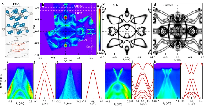
kx (π/a) Cut #1 Cut #4 Cut #3 Cut #2 Γ Z X b a PtSn4
FIG. 1. (color online) Experimental and calculated structure of the Fermi surface and band
dis-persion of PtSn4. a Crystal structure (Pt: white spheres, Sn: blue spheres) and Brillouin zone
of PtSn4. b Fermi-surface plot of ARPES intensity integrated within 10 meV of the chemical
potential along Γ−Z and Γ−X. c DFT-calculated bulk FS slice atky = 0.284π/b. d Calculated
surface FS with a 24-layer slab. eBand dispersion atkz = 0.88π/calong cut #1 inb. f Calculated
bulk-band dispersion atkz = 0.88π/c and ky = 0.284π/b. g Band dispersion atkz =π/calong cut
#2 inb. h Calculated bulk-band dispersion atkz =π/c andky = 0.284π/b. iBand dispersion at
kx = 0.88π/aalong cut #3 in b. j Calculated surface-band dispersion at kx = 0.88π/a with
42-layer slab. kBand dispersion atkx =π/aalong cut #4 inb. lCalculated surface-band dispersion
atkx=π/awith 42-layer slab.
Brillouin Zone (BZ) for PtSn4 are shown in Fig.1. Panel (b) shows the ARPES intensity
integrated within 10 meV of the chemical potential. High intensity areas mark the contours
of the FS sheets. The FS consists of at least one large electron pocket at the center of
BZ surrounded by several other electron and hole FS sheets, consistent with the quantum
oscillation result34. Fig.1cshows the calculated bulk FS, which matches the data well close
to the center of the zone and Z point in Fig.1b and it is also consistent with the calculated
FS using full potential linearized augmented plane wave (FLAPW) within local density
approximation (LDA)34. However, it does not predict the FS crossings close to theX point,
[image:5.612.91.518.74.300.2]0.2 -0.2
kx (π/a) #7
0.2 -0.2 k
x (π/a) #6
0.2 -0.2 k
x (π/a)
-0.2 -0.1 0.0 Energy (eV) #5 #4 #3 -0.2 -0.1 0.0 Energy (eV) #1 0.2 -0.2
kx (π/a) #8 #2 1.2 1.1 1.0 0.9 0.8 kz (π /c)
-0.1 0.0 0.1 kx (π/a)
#1 #8 Z 1.0 0.5 0.0 -0.5 -1.0 kz (π /c)
-0.5 0.0 0.5 kx (π/a) Z
Γ
a b
c - f
g - j
High
Low
FIG. 2. (color online) Fermi surface and band dispersion in the proximity of theZ point. aFermi
surface plot of ARPES intensity integrated within 10 meV of the chemical potential along Γ−Z.
b Zoom in image of the red box in Fig.2a, red dashed lines mark the cut #1 - #8. c - j Band
dispersion along cut #1 - #8. Cut #8 is cutting through the Z point. The red arrows mark the
Dirac nodes.
experimental features are well reproduced by calculation of surface states using slab method;
results of which are shown in Fig.1d. Band dispersion along several cuts in proximity of
Z and X points are shown in Fig.1e - l. Close to Z point (Figs.1e & g), the dispersion
resembles a Dirac-like feature, but the intensity within band contour points to bulk origin
and it is consistent with corresponding band calculations shown in Figs.1f, h. Close to X
point (Figs.1i & k), the band dispersion is also Dirac-like, but very sharp, thus more likely to
be due to surface states; moreover, it is consistent with the slab calculation shown in Figs.1j,
l. The data in Fig.1 demonstrates that the experimentally observed band structure has both
bulk and surface components. The former dominate the Fermi surface close to the Z point,
and the latter is prominent close to the X point. The linear dispersion and gapless band
crossings strongly suggest that both bulk and surface features at the edge of the Brillouin
[image:6.612.197.416.71.336.2]-0.4 -0.2 0.0 0.2 0.4 kz ( π /c) 1.5 1.0 0.5 0.0 -0.5
kx (π/a)
Γ X
#4 #3
#2
-0.2 0.0 0.2 kz (π/c)
-0.2 -0.1 0.0 Energy (eV) -0.2 0.0 0.2 kz ( π /c) 1.2 1.1 1.0 0.9 0.8
kx (π/a)
#1 #12
X
#5
-0.2 0.0 0.2 kz (π/c)
-0.2 -0.1 0.0 Energy (eV) #7 #6
-0.2 0.0 0.2 kz (π/c) #8
-0.2 0.0 0.2 kz (π/c) #9
-0.2 0.0 0.2 kz (π/c) #10
-0.2 0.0 0.2 kz (π/c) #11
-0.2 0.0 0.2 kz (π/c) #12
a b
c - h
i - n
High
Low
FIG. 3. (color online) Fermi Surface plot and band dispersion close to theXpoint. aFermi surface
plot of ARPES intensity integrated within 10 meV of the chemical potential along Γ−X. bZoom
in image of the red box in Fig.3a, red dashed lines mark the cut #1 - #12. c - n Band dispersion
along cut #1 - #12. Cut #8 is cutting through the X point. The red arrows mark the Dirac
nodes.
to Cd3As26, NbP9, WTe235,36.
In Fig.2 we focus on the interesting features near theZpoint in more detail. Fig.2bshows
an enlarged image from the red box in Fig.2a, where two triangular- shaped FS sheets are
observed. Figs.2c - j show the detailed evolution of band dispersions along cuts#1 to #8.
A sharp linear dispersion starts to cross at binding energy of ∼200 meV in Fig.2c and the
Dirac point moves up in energy in Figs.2d- 2gand finally reaches the Fermi level in Fig.2h,
as indicated by red arrows. Then, the Dirac point moves up above the Fermi level and
becomes a sharp, shallow hole pocket in Figs.2g - 2j. This movement of the Dirac nodes
forms a line in the Energy-Momentum space in the proximity ofZ.
Whereas the behavior described above has previously been predicted by theory, the
struc-ture in the proximity of the X point is far more interesting. We now examine the Fermi
surface and band dispersion in small area in the part of the Brillouin zone that is marked
by the red box in Fig.3a. The Fermi surface in this region consists of a short arc along
[image:7.612.130.485.75.307.2]-0.2 0.0 0.2 kz (π/c)
-0.2 -0.1 0.0
Energy (eV)
-0.2 0.0 0.2 kz (π/c)
-0.2 -0.1 0.0
Energy (eV)
kz (π/c) 123
Intensity (arb. units)
Intensity (arb. units)
-0.2 -0.1 0.0 Energy (eV) 1 3 2 50 40 30 20 10 0 Gap (meV) 100 80 60 40 20 Layers
a - c
d - f
g High i h Low -0.1 0.0 0.1 kz ( π /c) 1.1 1.0 0.9
kx (π/a) Dirac node arc at EF Dirac node arcs at EB=60 meV Dirac nodes at EB=90 meV
X 1st BZ
2nd BZ -0.3 -0.2 -0.1 0.0 Energy (eV)
-0.2 -0.1 0.0 0.1 0.2 kz (Å
-1 )
Gap
j
FIG. 4. (color online) Two types of gapless Dirac-like dispersion close toXpoint. aBand dispersion
along cut #1 in Fig.3b. b Momentum Dispersion Curves (MDC) of a. cEnergy Dispersion Curve
(EDC) along the red dashed line in b. d Band dispersion along cut #10 in Fig.3b. e Momentum
Dispersion Curves (MDC) of d. f Energy Dispersion Curves (EDC) along the red dashed lines in
e. g Calculated surface band at X with a 42-layer slab. h Energy-gap evolution with increasing
number of layers in the slab. i Locations of the Dirac nodes extracted from the peak positions of
the MDCs as marked by the red dashed lines in a and d. The blue dots denote the two single
Dirac nodes at EB = 90 meV. The green dots denote the two Dirac node arcs at EB = 60 meV.
The red dots denote the Dirac node arc at EF. j Schematic of Double Dirac node arc structure.
Red arrows mark the double single nodes and double node arcs.
Detailed band dispersion along cuts#1 to #12 are shown in Figs.3c - n. The data along cut
#1 shows Dirac-like dispersion, with the top and bottom bands merging at a single gapless
point. The band is very sharp, consistent with its surface origin. As we move closer to the
X point, two things happen: a gap develops between top and bottom bands and both top
and bottom bands split into two parts symmetric about thekz = 0 line (Figs.3d - f). Before
reaching theX point, the gap vanishes and there are two gapless Dirac-like features in close
proximity ofX point. The inner bands of the two Dirac features merge along symmetry line
[image:8.612.136.483.78.312.2]features extend along one direction in the proximity of the X point between kx = 0.95π/a
and kx = 1.05π/a. Outside of this momentum range a gap develops separating the upper
and lower portion of the band. This gives rise to two arcs of Dirac nodes located at binding
energy of ∼ 60 meV, which we named Dirac node arcs.
We now proceed to demonstrate that the Dirac-like dispersion shown in Fig.3 is gapless
by plotting the momentum-dispersion curves (MDCs) and energy-dispersion curves (EDCs).
Fig.4c shows the EDC extracted along the red dashed line in 4b. The red arrow marks the
peak located at roughly 90 meV below the Fermi level (Fig.4a), and demonstrates the
absence of an energy gap in this single Dirac-like feature. In Fig.4d, we show the double
Dirac-like features along cut#8(Fig.3j). The EDCs shown in 4f are extracted along the
red-dashed lines marked as 1, 2, 3 in Fig.4e. The red arrows in Fig.4e and Fig.4f mark
location of the peaks at binding energy of 60 meV, and show the gapless nature of these
dispersions. The surface-state calculation using 42-layer slab shows that the conduction and
valence bands are separated by roughly 23 meV in the single Dirac feature. However, further
increase in the layer number would dramatically reduces the gap size, as shown in Fig.4h.
To better illustrate the Dirac node arc structure, we plot the location of the Dirac nodes in
the momentum space in Fig.4iby extracting the peak positions of MDCs at each node (i.e.,
at the binding energy of 90 meV in the single Dirac dispersion and 60 meV at the proximity
of X point in the double Dirac dispersion, as marked by the red-dashed lines in Fig.4aand
d). In Fig.4j, the schematic of the double Dirac node arc structure is shown, with two Dirac
dispersion extending along one-dimension in momentum space.
In conclusion, we use ultrahigh resolution tunable VUV laser-based ARPES to measure
the Fermi surface and band dispersion of PtSn4. The most significant result is the discovery
of Dirac node arc structure in this material. Our results show that near the X point,
the single Dirac dispersion evolves into two gapped dispersions and, before reaching the
X point, the gaps close and two gapless Dirac-like feature emerge extending along one
dimension in momentum space, forming Dirac node arc. These novel features differ from
previously predicted Dirac line nodes that form closed loops in momentum space. We
proposed that this novel topological nodal structure could be an ideal platform for studying
the exotic properties of Dirac Fermions. Finally, we note that, most of the recently discovered
ultrahigh magnetoresistive materials31–33 seem to also possess Dirac or Weyl features in the
identifying novel topological states and relativistic behavior based on rudimentary transport
measurements.
METHODS
Sample growthSingle crystals of PtSn4 were grown out of a Sn-rich binary melt37. The
constituent elements, with an initial stoichiometry of Pt0.04Sn0.96, were placed in an alumina
crucible and sealed in a quartz tube under a partial Ar pressure. After the quartz ampoule
was heated up to 600 ◦C, the ampoule was cooled down to 350 ◦C over 60 h34. In order to
decant the Sn readily at this temperature, a frit-disc crucible was used38.
Sample preparation and measurements ARPES measurements were carried out
using a laboratory-based system consisting of a Scienta R8000 electron analyzer and a a
tunable VUV laser light source39. The data were acquired using a tunable VUV laser
ARPES system, consisting of a Scienta R8000 electron analyzer, picosecond Ti:Sapphire
oscillator and fourth harmaonic generator. All Data were collected with a constant photon
energy of 6.7 eV. Momentum and energy resolution were set at ∼ 0.005 ˚A−1 and 2 meV.
The size of the photon beam on the sample was ∼30 µm. Samples were cleaved in situ at
a base presure lower than 1×10⁻¹⁰ Torr. Samples were cooled using a closed cycle
He-refrigerator and the sample temperature was measured using a silicon-diode sensor mounted
on the sample holder. The energy corresponding to the chemical potential was determinded
from the Fermi edge of a polycrystalline Au reference in electrical contact with the sample.
Samples were cleave at 40K and were kept at the cleaving temperature throughout the
measurement.
Calculation method Density functional theory40,41 (DFT) calculations have been done
in VASP42,43 using PBE44 exchange-correlation functional, plane-wave basis set with
pro-jected augmented waves45 and spin-orbital coupling (SOC) effect included. For bulk band
structure of PtSn4, we use the conventional orthorhombic cell of 20 atoms with a
Monkhorst-Pack46 (8×6×8) k-point mesh. For surface band structure, we use slabs up to 96 atomic
layers or 320 atoms with a (8× 1×8) k-point mesh and at least a 12 ˚A vacuum. The
kinetic energy cutoff is 230 eV. The convergence with respect to k-point mesh was carefully
checked, with total energy converged, e.g., well below 1 meV/atom. We use experimental
bulk positions.
CORRESPONDING AUTHOR
Correspondence to: Adam Kaminski, email: [email protected]; Paul C. Canfield,
email: [email protected].
ACKNOWLEDGEMENTS
This work was supported by the U.S. Department of Energy, Office of Science, Basic
Energy Sciences, Materials Science and Engineering Division. Ames Laboratory is operated
for the U.S. Department of Energy by Iowa State University under contract No.
DE-AC02-07CH11358.
AUTHOR CONTRIBUTIONS
P.C. C. initiated the work by insisting that Y. W. and A. K. design and carry out the
experiment. Y. W., D. M. and L. H. acquired and analyzed ARPES data. L.-L. W., D.D.
J. and Y. L. provided the density functional calculations. E. M. grew the samples under the
supervision of S.L. B. and P.C. C.. Y. W. and A. K. wrote the draft of the manuscript. All
authors discussed and commented on the manuscript.
ADDITIONAL INFORMATION
Supplementary information is available in the online version of the paper. Reprints and
permissions information is available online at www.nature.com/reprints.
COMPETING FINANCIAL INTERESTS
REFERENCES
∗ Present address: Department of Physics, Simon Fraser University, Canada
1 Hasan, M. Z., Kane, C. L. Colloquium : Topological insulators. Rev. Mod. Phys.82, 3045–3067
(2010).
2 Burkov, A. A., Hook, M. D., Balents, L. Topological nodal semimetals. Phys. Rev. B 84,
235126 (2011).
3 Burkov, A. A., Balents, L. Weyl semimetal in a topological insulator multilayer. Phys. Rev.
Lett. 107, 127205 (2011).
4 Heikkil, T., Volovik, G. Dimensional crossover in topological matter: Evolution of the multiple
Dirac point in the layered system to the flat band on the surface. JETP Letters 93, 59–65
(2011).
5 Liu, Z. K., et al. Discovery of a three-dimensional topological Dirac semimetal, Na
3Bi. Science
343, 864–867 (2014).
6 Neupane, M., et al. Observation of a three-dimensional topological Dirac semimetal phase in
high-mobility Cd3As2. Nat Commun 5 (2014).
7 Xu, S.-Y., et al. Discovery of a weyl Fermion semimetal and topological Fermi arcs. Science
349, 613–617 (2015).
8 Xu, S., et al. Discovery of a weyl Fermion state with Fermi arcs in niobium arsenide. Nat Phys
11, 748–754 (2015).
9 Xu, S.-Y., et al. Experimental discovery of a topological weyl semimetal state in TaP. Science
Advances 1 (2015).
10 Geim, A. K., Novoselov, K. S. The rise of graphene. Nat Mater 6, 183–191 (2007).
11 Young, S. M.,et al. Dirac semimetal in three dimensions. Phys. Rev. Lett.108, 140405 (2012).
12 Wang, Z., et al. Dirac semimetal and topological phase transitions in A
3bi (a= Na, K, Rb).
13 Wang, Z., Weng, H., Wu, Q., Dai, X., Fang, Z. Three-dimensional Dirac semimetal and quantum
transport in Cd3As2. Phys. Rev. B 88, 125427 (2013).
14 Liu, Z. K., et al. A stable three-dimensional topological Dirac semimetal Cd
3As2. Nat Mater
13, 677–681 (2014).
15 Yi, H.,et al.Evidence of topological surface state in three-dimensional Dirac semimetal Cd
3As2.
Sci. Rep.4 (2014).
16 Borisenko, S., et al. Experimental realization of a three-dimensional Dirac semimetal. Phys.
Rev. Lett. 113, 027603 (2014).
17 Narayanan, A., et al. Linear magnetoresistance caused by mobility fluctuations in n-doped
Cd3As2. Phys. Rev. Lett.114, 117201 (2015).
18 Weyl, H. Elektron und gravitation. i. Zeitschrift fr Physik 56, 330–352 (1929).
19 Huang, S., et al. A weyl Fermion semimetal with surface Fermi arcs in the transition metal
monopnictide taas class. Nat Commun 6 (2015).
20 Weng, H., Fang, C., Fang, Z., Bernevig, B. A., Dai, X. Weyl semimetal phase in
noncentrosym-metric transition-metal monophosphides. Phys. Rev. X 5, 011029 (2015).
21 Weng, H.,et al. Topological node-line semimetal in three-dimensional graphene networks.Phys.
Rev. B 92, 045108 (2015).
22 Zeng, M., et al. Topological semimetals and topological insulators in rare earth monopnictides.
arXiv:1504.03492 (2015).
23 Yu, R., Weng, H., Fang, Z., Dai, X., Hu, X. Topological node-line semimetal and Dirac
semimetal state in antiperovskite Cu3PdN. Phys. Rev. Lett. 115, 036807 (2015).
24 Kim, Y., Wieder, B. J., Kane, C. L., Rappe, A. M. Dirac line nodes in inversion-symmetric
crystals. Phys. Rev. Lett.115, 036806 (2015).
25 Fang, C., Chen, Y., Kee, H.-Y., Fu, L. Topological nodal line semimetals with and without
spin-orbital coupling. Phys. Rev. B 92, 081201 (2015).
26 Bian, G., et al. Drumhead surface states and topological nodal-line Fermions in TlTaSe
2.
arXiv:1508.07521 (2015).
27 Xie, L. S.,et al. A new form of Ca
3P2with a ring of Dirac nodes.APL Mater.3, 083602 (2015).
28 Yamakage, A., Yamakawa, Y., Tanaka, Y., Okamoto, Y. Line-node Dirac semimetal and
topo-logical insulating phase in noncentrosymmetric pnictides CaAgX (X= P, As). arXiv:1510.00202
29 Bian, G., et al. Topological nodal-line Fermions in the non-centrosymmetric superconductor
compound PbTaSe2. arXiv:1505.03069 (2015).
30 Schoop, L. M., et al. Dirac cone protected by non-symmorphic symmetry and 3d Dirac line
node in ZrSiS. arXiv:1509.00861 (2015).
31 Liang, T.,et al.Ultrahigh mobility and giant magnetoresistance in the Dirac semimetal Cd
3As2.
Nat Mater 14, 280–284 (2015).
32 Shekhar, C.,et al. Extremely large magnetoresistance and ultrahigh mobility in the topological
weyl semimetal candidate NbP. Nat Phys 11, 645–649 (2015).
33 Ali, M. N., et al. Large, non-saturating magnetoresistance in WTe
2. Nature 514, 205–208
(2014).
34 Mun, E.,et al. Magnetic field effects on transport properties of PtSn
4.Phys. Rev. B 85, 035135
(2012).
35 Pan, X.-C., et al. Robust linear magnetoresistance in WTe
2. arXiv:1505.07968 (2015).
36 Wu, Y., et al. Temperature-induced lifshitz transition in WTe
2. Phys. Rev. Lett. 115, 166602
(2015).
37 Canfield, P. C., Fisk, Z. Growth of single crystals from metallic fluxes. Philosophical Magazine
Part B 65, 1117–1123 (1992).
38 Canfield, P. C., Kong, T., Kaluarachchi, U. S., Jo, N. H. Use of frit-disc crucibles for routine
and exploratory solution growth of single crystalline samples. arXiv:1509.08131 (2015).
39 Jiang, R., et al. Tunable vacuum ultraviolet laser based spectrometer for angle resolved
pho-toemission spectroscopy. Review of Scientific Instruments 85, 033902 (2014).
40 Hohenberg, P., Kohn, W. Inhomogeneous electron gas. Phys. Rev.136, B864–B871 (1964).
41 Kohn, W., Sham, L. J. Self-consistent equations including exchange and correlation effects.
Phys. Rev. 140, A1133–A1138 (1965).
42 Kresse, G., Furthm¨uller, J. Efficient iterative schemes for ab initio total-energy calculations
using a plane-wave basis set. Phys. Rev. B 54, 11169–11186 (1996).
43 Kresse, G., Furthmller, J. Efficiency of ab-initio total energy calculations for metals and
semi-conductors using a plane-wave basis set. Computational Materials Science 6, 15 – 50 (1996).
44 Perdew, J. P., Burke, K., Ernzerhof, M. Generalized gradient approximation made simple.
Phys. Rev. Lett. 77, 3865–3868 (1996).
46 Monkhorst, H. J., Pack, J. D. Special points for brillouin-zone integrations. Phys. Rev. B 13,
5188–5192 (1976).
47 Knnen, B., Niepmann, D., Jeitschko, W. Structure refinements and some properties of the
transition metal stannides Os3Sn7, Ir5Sn7, Ni0.402(4)Pd0.598Sn4,α-PdSn2 and PtSn4.Journal of