A Frame work on AMBA bus based Communication
Architecture to improve the Real Time Computing
Performance in MPSoC
M.Venkateswara Rao
Research Scholar Department of ECM K L UNIVERSITY A.P., IndiaT.V.Rama Krishna,
Ph.D ProfessorDepartment of ECE K L UNIVERSITY A.P., India
G. Yasaswini
PG Scholar Department of ECM K L UNIVERSITY A.P., IndiaABSTRACT
Enormous advancements in System-on-Chip (SoC) have led to a new area called as MPSoC, having single chip with many processors. MPSoC is usually targeted for high-end embedded designs to meet real-time requirements, where performance and bandwidth plays a major role. Multi Processor System-on-Chip (MPSoC) deals with multiple on-chip processors and processing elements that are essential for multi-core processors integrated onto the single chip. As more and more processors are integrated onto the same silicon chip, there should be proper communication and synchronization to ensure better performance. For this purpose, several Communication Architectures (CAs) have been developed like ARM AMBA, IBM Core Connect, Altera Avalon, and Open Cores Wishbone. One of the major challenges is to select a suitable architecture among the various MPSoC architectures. AMBA bus is widely used in the high-performance and high frequency SoC designs. This paper deals with several topologies and communication protocols. In this paper AMBA versions and their buses/interfaces are discussed.
Keywords
MPSoC, AMBA, AXI, CAs, AMBA5 CHI
.
1.
INTRODUCTION
Shrinking design sizes and tremendous changes in technologies have led to integrated circuits (ICs) including highly complex number of transistors. As a consequence, manufacturers are integrating increasing number of components on a chip. A system-on-a-chip (SoC) which is an integrated circuit includes many components of a computer or other electronic system into a single chip [1]. SoC includes many processors such as general purpose processors, digital purpose processors, or application specific intellectual property (IP) along with on-chip memories, I/O devices integrated on a single chip.
On-chip bus organized communication architecture (CA) is among the top challenges in CMOS SoC technology due to increase in number of components and the communication between them. The performance of SoC depends on the efficiency of its bus structure. Various available bus architectures from leading manufacturers are CoreConnect from IBM, AMBA from ARM, Wishbone from Open Core, Silicon Backplane from Sonics, Avalon bus from Altera, STBus by STMicroelectronics and others. ARM processor is mostly used in many bus architectures.The crucial factors including bus topologies, arbitration methods, bus widths are to be considered. Real time environments having
heterogeneous architectures, improves real time behavior by reducing conflicts among processing elements and tasks [2]. The rest of this paper is organized as follows: Section II describes about MPSoC. In Section III presents AMBA bus and its versions along with supporting buses/interfaces. The last section gives a comparison between AMBA protocols.
2.
MULTI PROCESSOR
SYSTEM-ON-CHIP (MPSOC)
An MPSOC is a System-on-chip incorporating many processors as system components (IP’s) that are necessary for any high-end applications. A multiprocessor is a tightly coupled system having one or more IP’s (Multiple Processors) each sharing on-chip memory and peripherals, in order to simultaneously process programs. Hence MPSoC’s are widely used in communication, multimedia and networking applications. Lucent Daytona was the first MPSoC designed with four CPU’s attached to a single bus. Applications having Power consumption, High throughput and Fast Processing time as the major constraints strictly depend on Multi Processor SoC designs. MPSoC’s are mostly used in workstations and servers involving dual-core and quad-core processors. Latest developments in MPSoC led to the usage of 10 cores called as deca-core processors. Increase in the number of processors per chip causes more difficulties for communication and synchronization between several IP’s to ensure better performance and utilization of the entire system [3].
3.
AMBA BUS
Advanced Microcontroller Bus Architecture (AMBA) is used as on-chip bus in most SoC designs. AMBA bus is widely used in portable mobile phones like smart phones. AMBA protocol is an open standard, introduced in 1996 by ARM. First AMBA buses were Advanced System Bus (ASB) and Advanced Peripheral Bus (APB). Second version of AMBA, added Advanced High Performance Bus (AHB). In 2003, AMBA3 was introduced with Advanced Extensible Interface (AXI) for even high performance interconnect and Advanced Trace Bus (ATB) as part of core-sight on-chip and trace solution. In 2010, AMBA4 AXI4 was introduced, then in 2011 extended in system wide coherency with AMBA4 ACE. Recently in June 2013, ARM introduced AMBA5 Coherent Hub Interface (CHI) specification was introduced, with a re-designed high-speed transport layer and features re-designed to reduce congestion [4].
System-on-Chip (SoC). The objective of AMBA bus is as follows:
For facilitating first-time-right SoC design with one or more Processors (application-specific or general purpose).
Allows IP re-use of IP cores, peripherals and system macro cells.
Supports high performance and low-power on-chip communication between components by minimizing silicon infrastructure [5].
3.1
AMBA 2.0 Protocol
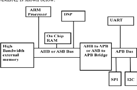
AMBA2 defines on-chip communication standards for high performance embedded designs by including three buses/interfaces as follows:
Advanced High Performance Bus (AHB)- widely used in ARM7,ARM9, and ARM Cortex-M designs.
Advanced System Bus(ASB) and
Advanced Peripheral Bus(APB2 or APB)
Advanced High-Performance Bus (AHB)
AMBA AHB is designed for high performance, high clock frequency system modules.AHB acts as high-performance backbone bus in AMBA2 design.AHB supports efficient interconnection of high-performance processors, on-chip memories, off-chip memories interfaces with low-power peripheral modules [6].
AHB features are as follows:
Pipelined Operations
Burst Transactions
Single edge Clock Protocol
Several Bus Masters
Large Bus-widths(64/128 bit)
Single-cycle bus master handover.
Only one transaction at a time-either Read or Write.
Supports 16 masters for initiating bus transactions and 16 slaves for responding to transactions initiated by a master [6].
A simple transaction on the AHB bus consists of an address phase and a subsequent data phase. Access to the target device is controlled through a MUX, there by admitting bus-access to only one master at a time. AHB bus integrates high performance modules like processors (ARM, DSP, AVR) and memories [7].
Advanced System Bus (ASB)
ASB is also used for interconnection of processors, memories.AHB or ASB bus is connected to APB bus using a Bridge component.ASB is similar to AHB bus except that AHB supports Burst and Split transactions.
Advanced Peripheral Bus (APB)
AMBA APB supports low power consumption and reduced interface complexity for supporting low power components like UART,SPI,I2C,Timer etc., APB is especially designed for low bandwidth control accesses.APB bus supports 33MHz and 66 MHz signals[6].
[image:2.595.317.542.146.294.2]AMBA2 is shown below:
Fig 1: AMBA 2.0 Protocol
3.2
AMBA 3.0 Protocol
AMBA 3 Specification has four buses/interfaces as follows:
Advanced eXtensible Interface(AXI3 or AXI v1.0) – widely used on latest ARM Cortex-A Processors including Cortex-A9
Advanced High Performance Bus Lite(AHB-Lite v1.0)
Advanced Peripheral Bus(APB3 v1.0)
Advanced Trace Bus(ATB v1.0)
Advanced eXtensible Interface (AXI3)
AXI is targeted to achieve high performance, high clock frequency system designs aiming high speed sub-micron interconnect.
AXI Protocol is burst-based. Every transaction involves both address and control information in the address channel that describes the nature of the data that is to be transferred. Data can be transferred using write and read data channels between master and slave. The write transactions involve all the data in the direction from the master to the slave.AXI protocol has an additional write response channel for indication to the master, the completion of the write transaction by the slave [7]. AXI3 supports five channels namely:
Read Address Channel
Read Data Channel
Write Address Channel
Write Data Channel
Write Response Channel
Fig 2: AXI3 channels
3.2.1
Read and Write Address Channel
Read and write transactions have their own address channels. The address channel consists of address and control information regarding to that transaction.
AXI3 address channel supports the following features using several signals.
Supports variable-length bursts, from 1 to 16 data transfers per burst (AxLEN signal).
Supports bursts with a transfer size of 8-1024 bits (AxSIZE signal).
It has wrapping, incrementing, and non-incrementing bursts (AxBURST signal).
Performs atomic operations, using exclusive or locked accesses (AxLOCK signal) [6].
3.2.2
Read Data Channel
Read Data Channel includes Read data and Read Response information. This channel includes:
Data bus widths of sizes 8,16,32,64,128,256,512, or 1024 bits (RDATA).
Read Response channel for indicating the completion status of the Read Transaction.
3.2.3
Write Data Channel
Write Data Channel contains the Write Data from the master to the slave. This Channel includes:
Data bus widths of sizes 8,16,32,64,128,256,512, or 1024 bits (WDATA).
Includes one byte strobe for every byte, for indicating which bytes of the data bus are valid (WSTRB).
Last transaction inside the burst must be signaled through WLAST Signal.
3.2.4
Write Response Channel
The Write Response Channel provides a way for the slave to respond to the Write transactions. All write transactions uses completion signaling. The completion signal occurs once for each burst, not for every individual data within each burst [7].
3.2.5
Read Transaction
[image:3.595.317.545.131.277.2]The following is the figure that shows Read transaction between master and slave involving Read Address channel and Read Data Channel.
Fig 3: Read Transaction
3.2.6
Write Transaction
Write transactions uses Write Address, Write Data and Write Response Channels as shown below:
Fig 4: Write transaction
3.2.7
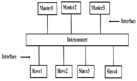
Interface and Interconnect
The system including several masters and slaves devices connected by some form of interconnect is shown below:
Fig 5: Interface and Interconnect
[image:3.595.317.567.335.488.2] [image:3.595.316.547.550.687.2] Between a master and the interconnect
Between a slave and the interconnect
Between a master and a slave [7].
AMBA AXI3 protocol features are as follows:
Suitable for high bandwidth and low latency designs.
Having separate address and data phases.
System level Cache Support.
Protection Unit Support.
Unaligned Data transfers using Byte strobes.
Supports Burst transactions with only start address issued.
Out-of-order transaction Completion
Can handle multiple addresses [6].
3.3
AMBA 4.0 Protocol
AMBA version 4.0 supports following buses/interfaces:
AXI Coherency Extensions(ACE)- widely used in ARM Cortex-A processors including Cortex-A7 and Cortex-A15
AXI Coherency Extensions Lite(ACE-Lite)
Advanced eXtensible Interface Lite 4 (AXI4-Lite)
Advanced eXtensible Interface 4 (AXI4)
Advanced eXtensible Interface Stream(AXI4-Stream v1.0)
Advanced Peripheral Bus(APB4 v2.0)
Advanced Trace Bus(ATB v1.1)
Advanced eXtensible Interface 4 (AXI4)
AMBA 4.0 releases second version of AXI, AXI4 in 2010.There is three types of AXI interfaces as follows:
AXI4: used for high performance memory-mapped requirements.
AXI4-Lite: Used for simple, low throughput memory-mapped communication.
AXI4-Stream: Used for high-speed streaming data.
The following are the features for AXI4 other than AXI3:
Removal of locked transactions.
Removal of Write Interleaving. Is supported.
Additional Quality of Service (QoS) signaling.
Updates Write Response requirements.
Support of up to 256 beats of burst lengths.
Updated AWCACHE and ARCACHE signaling details [8].
Advanced eXtensible Interface 4-Lite (AXI4-Lite) AXI4-Lite is a subset of the AXI4 protocol intended for communication with simpler, smaller control register-style interfaces in components.
Features of AXI4-Lite are as follows:
Exclusive transactions are not supported.
All transactions are supported to length of one.
All accesses are modifiable and Non-bufferable.
Supports a data bus of widths 32-bit and 64-bit.
All data accesses are the same size as of data bus width [9].
Advanced eXtensible Interface 4- Stream (AXI4-Stream) AXI4-Stream protocol is designed especially for unidirectional data transfers from master to the slave with greatly reduced signal routing.
AXI4-Stream Protocol features are as follows:
Ideal for implementation in FPGA.
Supports single and multiple data streams using the same set of shared wires.
Support for multiple data widths within the same interconnect.
Axi4-Stream IP can be better optimized for performance in data flow applications [10].
AXI Coherency Extensions (ACE)
ACE, defined under AMBA 4 specification, extends AXI with additional signaling introducing system wide coherency.ACE adds three new channels between ACE master caches and hardware control of cache maintenance for sharing data.ACE also adds barrier support to enforce ordering of multiple outstanding transactions, thus minimizing CPU stalls waiting for preceding transaction to complete. ACE has additional channels that enable communication with a cached master when another master is accessing an address location that might be shared [9].
AXI Coherency Extensions Lite(ACE-Lite)
ACE-Lite protocol is small subset of ACE signals that offer I/O, or one-way, coherency, where ACE masters maintain the cache coherency of ACE-Lite masters. ACE-Lite masters can still snoop ACE master caches, but other masters cannot snoop ACE-Lite master's caches. ACE-Lite also supports barriers [8].
3.4
AMBA 5.0 Protocol
Coherent Hub Interface (CHI)
AMBA5 CHI architecture specification defines the interfaces for connection of fully coherent processors, such as Cortex-A57 and Cortex-A53processors and the CoreLink DMC-520 Dynamic Memory Controller. It is also used by the CoreLink CCN-504 Cache Coherent Network, which is capable of 1 Terabit/s data flows.ARM announced AMBA5 CHI which will enable ARM Cortex-A50 series processors to work together in high-performance, coherent processing “hubs”, and to deliver the high data rates that are common in Enterprise markets, such as servers and networking.
AMBA 5 CHI Support for:
Support for high frequency, non-blocking coherent data transfer between many processors
Quality of Service (QoS) to ensure optimal overall system performance across all masters
A layered model to allow separation of communication and transport protocols [11].
4.
COMPARITIVE STUDY OF AMBA
BUS PROTOCOLS
Table1: Comparison of AMBA bus Protocols
APB AHB AXI3 AXI4
Processors All ARM 7,9, Cortex-M ARM 11, ARM Cortex-A9 Cortex-A7 and Cortex-A15 No. of Masters
1 1-15 1-16 1-16
No. of Slaves 1-15 1-15 1-16 1-16
Burst length 1 1-32 1-16 1-16
Simultaneous read and write
No No Yes Yes
Control Signals
4 27 77 77
Pipelined operations
No Yes Yes Yes
Phases Setup, Enable Bus Request, Address, Data Address, Data, Response Address, Data, Response Quality of Service signaling (QoS)
No No No Yes
Out-of-order data transactions
No No Yes Yes
Address issues Separate address for every data item Separate address for every data item Burst based-One address per burst Burst based-One address per burst Transactions at a time
Only one Only one Multiple
Multiple
5.
CONCLUSION AND FUTURE SCOPE
MPSoC designs are the advanced techniques used mainly for real time high-end applications. The major factors to be considered while designing are power consumption, area, cost, performance, and bandwidth, and a proper balance between them should be maintained. Mostly used on-chip communication architecture is AMBA bus. Several improvements over AMBA versions have led to tremendous increase over performance issues. In this paper, we have discussed the existing versions of AMBA along with AMBA AXI, which is targeted to achieve high performance, high frequency SoC designs with high-speed sub-micron interconnect. Also we have compared AMBA Protocols. Recently CHI was introduced aiming at reducing congestion and ensuring high data rates in servers and networking.
6.
REFERENCES
[1] T. Ananth Kumar, DR.S. Saraswathi Janaki, “Design of AXI Bus For 32-bit Processor using Bluespec”, ISSN: 2278 – 1323 International Journal of Advanced Research in Computer Engineering & Technology, Volume 1, Issue 3, May 2012
[2] Wayne Wolf,Fellow, IEEE, Ahmed Amine Jerraya, and Grant Martin, Senior Member, IEEE, “MultiProcessor System On-Chip(MPSoC)Technology”, IEEE TRANSACTIONS ON COMPUTER-AIDED DESIGN OF INTEGRATED CIRCUITS AND SYSTEMS, VOL. 27, NO. 10, OCTOBER 2008.
[3] Wayne Wolf, Department of Electrical Engineering, “The Future of Multiprocessor Systems-on-Chips”, DAC 2004, June 7-11, 2004, San Diego, California, USA Copyright 2004, ACM 1-58113-828-8/04/0006.
[4] Advanced Microcontroller Bus Architecture available at http://en.wikipedia.org/wiki/Advanced_Microcontroller_ Bus_Architecture
[5] ARM, “AMBA Specification Overview 1997”, available at
http://www.arm.com.
[6] ARM, “AMBA Specification (Rev 2.0)”, available at http://www.arm.com
[7] Anurag Shrivastava, G.S. Tomar, Ashutosh Kumar Singh, “Performance Comparison of AMBA Bus-Based System-On-Chip Communication Protocol”, International Conference on Communication Systems and Network Technologies, 2011.
[8] ARM, “AMBA AXI and ACE Protocol Specification, 2011”, available at http://www.arm.com.
[9] AMBA open specifications available at http://www.arm.com/products/system-ip/amba/amba-open-specifications.php?tab=Specifications
[10]Xilinx, “AXI Reference Guide, March 2011”, available at http://www.xilinx.com.