Analysis of Power Supply Networks in VLSI Circuits
Don Stark
Tech Report WRL-TR-91-3
c
Copyright 1991
Contents
1 Introduction 1
1.1 System Overview : : : : : : : : : : : : : : : : : : : : : : : : : : : : : 2
1.2 Test Circuits : : : : : : : : : : : : : : : : : : : : : : : : : : : : : : : : 4
2 Resistance Extraction 6
2.1 Underlying Field Theory: : : : : : : : : : : : : : : : : : : : : : : : : : 7
2.2 One Dimensional Current Flow : : : : : : : : : : : : : : : : : : : : : : 9
2.3 Polygonal Decomposition Implementation: : : : : : : : : : : : : : : : : 11
2.3.1 An Overview of Magic’s Database : : : : : : : : : : : : : : : : 11
2.3.2 Database Preprocessing : : : : : : : : : : : : : : : : : : : : : : 15
2.3.3 Resistance Calculation : : : : : : : : : : : : : : : : : : : : : : : 18
2.4 Finite Differences : : : : : : : : : : : : : : : : : : : : : : : : : : : : : 20
2.4.1 Physical Analogs of Finite Differences : : : : : : : : : : : : : : 22
2.4.2 Solving the Equations : : : : : : : : : : : : : : : : : : : : : : : 24
2.5 Finite Elements : : : : : : : : : : : : : : : : : : : : : : : : : : : : : : 26
2.5.1 Rectangular Elements : : : : : : : : : : : : : : : : : : : : : : : 29
2.5.2 Boundary Conditions : : : : : : : : : : : : : : : : : : : : : : : 30
2.6 Finite Element Implementation : : : : : : : : : : : : : : : : : : : : : : 31
2.6.1 Region Subdivision : : : : : : : : : : : : : : : : : : : : : : : : 31
2.6.2 Subregion Library : : : : : : : : : : : : : : : : : : : : : : : : : 33
2.6.3 Mesh Generation: : : : : : : : : : : : : : : : : : : : : : : : : : 35
2.6.4 System Solution : : : : : : : : : : : : : : : : : : : : : : : : : : 39
3 Current Estimation for CMOS 45
3.1 Introduction : : : : : : : : : : : : : : : : : : : : : : : : : : : : : : : : 46
3.2 Previous Work : : : : : : : : : : : : : : : : : : : : : : : : : : : : : : : 48
3.2.1 Timing Analysis : : : : : : : : : : : : : : : : : : : : : : : : : : 48
3.2.2 Probabilistic Analysis : : : : : : : : : : : : : : : : : : : : : : : 51
3.3 Switch Level Simulation : : : : : : : : : : : : : : : : : : : : : : : : : : 56
3.3.1 Implementation : : : : : : : : : : : : : : : : : : : : : : : : : : 57
3.3.2 Current Waveform Generation: : : : : : : : : : : : : : : : : : : 61
3.3.3 Image Currents : : : : : : : : : : : : : : : : : : : : : : : : : : 65
3.3.4 Coupling Capacitance : : : : : : : : : : : : : : : : : : : : : : : 67
3.3.5 Charge Sharing : : : : : : : : : : : : : : : : : : : : : : : : : : 71
3.3.6 Glitches : : : : : : : : : : : : : : : : : : : : : : : : : : : : : : 74
3.4 Performance : : : : : : : : : : : : : : : : : : : : : : : : : : : : : : : : 75
4 Current Estimation for ECL 78
4.1 Introduction : : : : : : : : : : : : : : : : : : : : : : : : : : : : : : : : 79
4.2 Basic Current Tracing : : : : : : : : : : : : : : : : : : : : : : : : : : : 80
4.3 Advanced Structures : : : : : : : : : : : : : : : : : : : : : : : : : : : : 85
4.3.1 Switched and Split Currents : : : : : : : : : : : : : : : : : : : : 85
4.3.2 Logic Dependent Circuits : : : : : : : : : : : : : : : : : : : : : 87
4.3.3 Diode Decoders : : : : : : : : : : : : : : : : : : : : : : : : : : 89
4.3.4 Other Circuits : : : : : : : : : : : : : : : : : : : : : : : : : : : 91
4.4 Pattern Selection : : : : : : : : : : : : : : : : : : : : : : : : : : : : : : 92
4.5 Performance : : : : : : : : : : : : : : : : : : : : : : : : : : : : : : : : 94
5 Network Solution 99
5.1 Previous Work : : : : : : : : : : : : : : : : : : : : : : : : : : : : : : : 100
5.2 Trees of Resistors : : : : : : : : : : : : : : : : : : : : : : : : : : : : : 104
5.3 Simple Loops and Kirchoff’s Voltage Law : : : : : : : : : : : : : : : : 104
5.4 Series Connections of Resistors : : : : : : : : : : : : : : : : : : : : : : 109
5.4.1 Equivalent Circuit for Series Resistors : : : : : : : : : : : : : : 109
5.5 Network Solution Techniques : : : : : : : : : : : : : : : : : : : : : : : 114
5.5.1 Direct Methods : : : : : : : : : : : : : : : : : : : : : : : : : : 114
5.5.2 Iterative Methods : : : : : : : : : : : : : : : : : : : : : : : : : 116
5.6 Results : : : : : : : : : : : : : : : : : : : : : : : : : : : : : : : : : : : 116
5.7 Conclusions : : : : : : : : : : : : : : : : : : : : : : : : : : : : : : : : 118
6 Results 120
7 Conclusions 130
A Triangular Finite Element Derivation 134
List of Tables
1 Summary of Test Circuits : : : : : : : : : : : : : : : : : : : : : : : : : 5
2 Extraction Times for Example Circuits : : : : : : : : : : : : : : : : : : 41
3 Previous Solution Library Efficacy : : : : : : : : : : : : : : : : : : : : 42
4 Example Circuit Extraction Times : : : : : : : : : : : : : : : : : : : : : 43
5 Comparison of Current Pulses for Various Input and Output Slopes : : : 64
6 Comparison of Nodes and Coupling Capacitors in Test Circuits : : : : : 71
7 Importance of Glitch Currents : : : : : : : : : : : : : : : : : : : : : : : 75
8 Rsim Running Times for Test Circuits : : : : : : : : : : : : : : : : : : 75
9 Time Spent in Various Operations During Logging : : : : : : : : : : : : 76
10 Current Pulse Processing Times : : : : : : : : : : : : : : : : : : : : : : 77
11 Comparison of Current Pattern Selection Methods : : : : : : : : : : : : 96
12 Running Times for ECL Current Estimation : : : : : : : : : : : : : : : 96
13 Original and Mutual Resistance Matrices : : : : : : : : : : : : : : : : : 108
14 Subgraph Sizes for Various Networks : : : : : : : : : : : : : : : : : : : 108
15 Direct Method Solution Times : : : : : : : : : : : : : : : : : : : : : : : 118
16 Iterative Method Solution Times: : : : : : : : : : : : : : : : : : : : : : 118
List of Figures
1 System Overview : : : : : : : : : : : : : : : : : : : : : : : : : : : : : 3
2 Resistive Region Model : : : : : : : : : : : : : : : : : : : : : : : : : : 8
3 Current Distribution Near Disturbances : : : : : : : : : : : : : : : : : : 9
4 Uniform Current Region : : : : : : : : : : : : : : : : : : : : : : : : : : 10
5 A Plane of Magic Tiles : : : : : : : : : : : : : : : : : : : : : : : : : : 12
6 Abstract Types : : : : : : : : : : : : : : : : : : : : : : : : : : : : : : : 14
7 Cell Overlap : : : : : : : : : : : : : : : : : : : : : : : : : : : : : : : : 15
8 Dissolving Contacts : : : : : : : : : : : : : : : : : : : : : : : : : : : : 16
9 Modifying Horizontal Strips : : : : : : : : : : : : : : : : : : : : : : : : 17
10 Interacting Concave Corners : : : : : : : : : : : : : : : : : : : : : : : : 18
11 Extraction Example : : : : : : : : : : : : : : : : : : : : : : : : : : : : 20
12 Finite Difference Mesh : : : : : : : : : : : : : : : : : : : : : : : : : : 22
13 Lumped Analog of Finite Difference Equations : : : : : : : : : : : : : : 23
14 Node Elimination : : : : : : : : : : : : : : : : : : : : : : : : : : : : : 25
15 Approximation of a Potential Surface : : : : : : : : : : : : : : : : : : : 27
16 Matching Current Flow Across Boundaries : : : : : : : : : : : : : : : : 27
17 Triangular Finite Element : : : : : : : : : : : : : : : : : : : : : : : : : 29
18 Rectangular Finite Element : : : : : : : : : : : : : : : : : : : : : : : : 30
19 Adding Breaklines to Regions : : : : : : : : : : : : : : : : : : : : : : : 32
20 Implementing Region Subdivision : : : : : : : : : : : : : : : : : : : : : 32
21 Possible Rotations of a Region : : : : : : : : : : : : : : : : : : : : : : 33
22 Region Scale Invariance : : : : : : : : : : : : : : : : : : : : : : : : : : 34
24 Subdivision of Elements : : : : : : : : : : : : : : : : : : : : : : : : : : 37
25 A Mesh Generation Example : : : : : : : : : : : : : : : : : : : : : : : 38
26 Finite Elements Used in Generation : : : : : : : : : : : : : : : : : : : : 39
27 Order of Node Elimination : : : : : : : : : : : : : : : : : : : : : : : : 40
28 Accuracy of Resistance Extraction : : : : : : : : : : : : : : : : : : : : 43
29 Simple Current Example : : : : : : : : : : : : : : : : : : : : : : : : : : 46
30 Effects of Capacitance on Currents : : : : : : : : : : : : : : : : : : : : 47
31 Timing Analysis Example : : : : : : : : : : : : : : : : : : : : : : : : : 49
32 Decoder Current Estimation : : : : : : : : : : : : : : : : : : : : : : : : 51
33 Probabilistic Analysis Example : : : : : : : : : : : : : : : : : : : : : : 52
34 CREST Current Waveform : : : : : : : : : : : : : : : : : : : : : : : : 54
35 An Example And-Or-Invert Gate : : : : : : : : : : : : : : : : : : : : : 58
36 Charging Paths for And-Or-Invert Gate : : : : : : : : : : : : : : : : : : 60
37 Current for And-Or-Invert Gate : : : : : : : : : : : : : : : : : : : : : : 60
38 Current Pulse Generated for an Event : : : : : : : : : : : : : : : : : : : 62
39 Pulses for Various Input and Output Slopes : : : : : : : : : : : : : : : : 63
40 Typical Input/Output Slope Distribution : : : : : : : : : : : : : : : : : : 64
41 Effects of Ignoring Image Current : : : : : : : : : : : : : : : : : : : : : 65
42 Bounding Box Current Estimation : : : : : : : : : : : : : : : : : : : : : 66
43 Re-Extraction Current Estimation : : : : : : : : : : : : : : : : : : : : : 68
44 Accuracy of Image Current Estimation : : : : : : : : : : : : : : : : : : 68
45 Effects of Coupling Capacitance : : : : : : : : : : : : : : : : : : : : : : 69
46 Distribution of Capacitance Bottom Plate : : : : : : : : : : : : : : : : : 70
47 Currents in a Pure Charge Sharing Event : : : : : : : : : : : : : : : : : 72
48 A Driven Charge Sharing Event : : : : : : : : : : : : : : : : : : : : : : 72
49 Relative Importance of Charge Sharing Events : : : : : : : : : : : : : : 73
50 Effects of a Node Glitch : : : : : : : : : : : : : : : : : : : : : : : : : : 74
51 Effects of Noise on ECL Circuits : : : : : : : : : : : : : : : : : : : : : 79
52 Currents for an ECL Gate : : : : : : : : : : : : : : : : : : : : : : : : : 81
53 Locations of Currents for a Single Gate : : : : : : : : : : : : : : : : : : 82
55 Temperature Compensation Circuit : : : : : : : : : : : : : : : : : : : : 83
56 Tracing of Currents : : : : : : : : : : : : : : : : : : : : : : : : : : : : 84
57 Switched and Unswitched Currents : : : : : : : : : : : : : : : : : : : : 86
58 Resistor Divided Currents : : : : : : : : : : : : : : : : : : : : : : : : : 87
59 Barrel Shifter : : : : : : : : : : : : : : : : : : : : : : : : : : : : : : : 88
60 Decoder Output Shared Current Line : : : : : : : : : : : : : : : : : : : 89
61 Diode Decoder Circuit : : : : : : : : : : : : : : : : : : : : : : : : : : : 90
62 Equivalent Circuits for Diode Outputs: : : : : : : : : : : : : : : : : : : 91
63 Tree Path Resistance Example : : : : : : : : : : : : : : : : : : : : : : : 94
64 Spanning Tree Estimate of Path Resistance : : : : : : : : : : : : : : : : 95
65 Effects of Path Resistance Estimate on Voltages : : : : : : : : : : : : : 97
66 Current Pattern Dependence of ECL circuits : : : : : : : : : : : : : : : 98
67 A Single Link Resistor in a Tree : : : : : : : : : : : : : : : : : : : : : 100
68 Tyagi’s Algorithm for Treelike Systems : : : : : : : : : : : : : : : : : : 101
69 Chowdhury’s Max Current Estimation Algorithm : : : : : : : : : : : : : 103
70 Overestimation in Chowdhury’s Algorithm : : : : : : : : : : : : : : : : 103
71 A Typical Power Network : : : : : : : : : : : : : : : : : : : : : : : : : 104
72 Solving for the Tree Voltages : : : : : : : : : : : : : : : : : : : : : : : 105
73 Multiple Link Resistors in a Tree : : : : : : : : : : : : : : : : : : : : : 106
74 Power Network with Trees and Simple Loops Removed : : : : : : : : : 109
75 Series Equivalent Circuit : : : : : : : : : : : : : : : : : : : : : : : : : 110
76 Series Circuit Example : : : : : : : : : : : : : : : : : : : : : : : : : : 111
77 Voltages for Series Circuit Example : : : : : : : : : : : : : : : : : : : : 112
78 Series and Equivalent Circuit : : : : : : : : : : : : : : : : : : : : : : : 113
79 Results of Network Reduction : : : : : : : : : : : : : : : : : : : : : : : 117
80 MIPS-X Ground Bus Voltage Plot : : : : : : : : : : : : : : : : : : : : : 124
81 uTitan Ground Bus Voltage Plot : : : : : : : : : : : : : : : : : : : : : : 125
82 uTitan Current Densities (rms): : : : : : : : : : : : : : : : : : : : : : : 126
83 SPIM Ground Bus Voltage Plot : : : : : : : : : : : : : : : : : : : : : : 127
84 SPIM Current Densities (rms) : : : : : : : : : : : : : : : : : : : : : : : 128
Chapter 1
Introduction
When at last this little instrument appeared, consisting, as it does, of parts every one of which is familiar to us, and capable of being put together by an amateur, the disappointment arising from its humble appearance was only partially relieved on finding that it was really able to talk.
James Clerk Maxwell
The Telephone (1878)
Although Maxwell was describing one of the technological marvels of his time, the telephone, rather than one of our time, the integrated circuit, his observation would not be out of place today. From a systems perspective, the operation of an individual transistor or resistor is quite simple, yet, considered in the aggregate, the operation of the entire circuit is quite remarkable. As the number of devices in a design increases, however, the relative simplicity of the individual devices is belied by the complexity of their collective behavior. Insuring that a million transistors are correctly arranged and interconnected is a nontrivial task. Designers have developed an array of tools to handle this increasing complexity, including simulators to check that the circuit implements the logic function desired, design rule checkers to verify that components are arranged in permissible topologies, and circuit extractors to see that the devices on chip are interconnected as the designer intended.
analysis tools exist. A set of these constraints surround the design’s power distribution system. To distribute power to all the devices on chip, each design includes a network of wires; if this network is not designed properly, the system will not operate as desired. Ex-cessive voltage drops along this network will slow down the circuit, and, if high enough, even cause it to switch incorrectly. High current density in these power connections can also cause circuit failure via electromigration. Metal interconnect in VLSI circuits is designed to withstand an average current density of about 1mA=m
2 and a peak current
density of approximately 10mA=m
2 [19]. At current densities above these values, the
electron wind will rearrange the metal ions, causing the metal to thin in some places and accumulate in others. Eventually, the chip will fail due to either an open or short circuit. As systems are scaled, these voltage and current problems are exacerbated.
The analysis tool described in this thesis, Ariel1, is designed to fill this gap. Given
a design in either a CMOS or a silicon ECL technology, Ariel will extract a a set of resistors to represent the power network, analyze the circuit to calculate when and where currents enter this resistance network, and solve the resulting system of equations. This information allows to the designer to see if the power network has sufficient capacity for the circuits it must supply.
1.1
System Overview
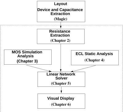
Power supply analysis is conducted in several stages, as shown in Figure 1. The first two steps, layout and extraction, are performed using the Magic layout editor[44]. These produce a mask level description of the design and its corresponding netlist, including parasitic capacitances. The remaining steps (inside the dotted box) are performed by Ariel, and are the scope of this thesis. These steps fall into three categories, corresponding to the three parts of Ohm’s law: resistance extraction, current estimation, and voltage calculation.
In the next chapter, I describe techniques for efficiently extracting resistances, paying special attention to problems inherent in power supply networks. Included in the system
1The name has two meanings. Ariel is the spirit who carries out commands for the magician Prospero
are two extractors: a fast, simple one that assumes uniform current flow, and a slower, more accurate one based on finite elements.
Device and Capacitance
Extraction
(Magic)
Layout
ECL Static Analysis
(Chapter 4)
MOS Simulation
Analysis
(Chapter 3)
Resistance
Extraction
(Chapter 2)
Linear Network
Solver
(Chapter 5)
Visual Display
[image:12.612.126.526.167.531.2](Chapter 6)
Figure 1: System Overview
Chapter Three investigates current estimation for CMOS circuits. Currents in CMOS are dynamic and pattern dependent; an accurate current estimator must take both these factors into account. After discussing algorithms adopted by other researchers, I describe my approach, which is based on timing simulation.
arranging these in a conservative distribution.
Chapter Five examines techniques for solving the resulting large system of equations. I investigate some configurations peculiar to power networks, and develop techniques for partitioning the network into smaller, more easily solved sections based on these configurations. Methods for efficiently solving the remaining portions of a network are also investigated.
In Chapter Six, I analyze several fairly large designs using the system. This analysis uncovered several mistakes made by the chips’ designers, which are visible on plots of the voltage and current density distributions. Possible improvements in the voltage and current distributions for the designs are also discussed.
1.2
Test Circuits
Throughout the thesis, several chips are used as test cases for the system. Analyzing large designs helps insure that the algorithms developed are practical for use on real systems. There are six chips in the test set: three CMOS designs from Stanford and Digital Equipment Corporation, and three ECL designs from MIPS Computer Systems. Table 1 summarizes their sizes, speeds, and technologies. The features of these systems are:
1. MIPS-X[24] is a 32-bit RISC microprocessor designed at the Computer Systems Lab of Stanford University by Mark Horowitz and a team of students. It is designed in a 2m, two-level-metal, n-well CMOS technology, and runs at a clock speed of
20MHz.2
2. Titan is also a 32-bit RISC Microprocessor, designed at the Digital Equipment
Corporation Western Research Laboratory by Norman Jouppi[28]. It is designed in a 1.5m, two-level-metal process, and runs at a speed of 25Mhz.
3. SPIM is a 64 by 64 iterating array multiplier designed by Mark Santoro of Stanford University[51]. It is designed in a 1.6m two-level-metal, CMOS technology, and
2The on-chip instruction cache was not included in any of the analyses; the device count listed in the
runs at 85MHz.
4. The R6000, R6010, and R6020 form an ECL chipset designed by David Roberts, Tim Layman, and George Taylor at MIPS Computer Systems[48]. All are designed in Bipolar Integrated Technology’s 2m, triple diffused ECL, three-level-metal
process, and run at 66.7MHz. The R6000 is a 32-bit microprocessor with on-chip TLB, the R6010 a 64-bit floating point controller, and the R6020 a system bus controller chip.
Circuit Devices Speed Technology
MIPS-X 47130 20MHz 2.0uM CMOS
uTitan 179390 25MHz 1.5uM CMOS
SPIM 41804 85MHz 1.6uM CMOS
R6000 CPU 149619 66.7MHz 2.0uM ECL
R6010 FPC 148745 66.7MHz 2.0uM ECL
R6020 SBC 163925 66.7MHz 2.0uM ECL
Chapter 2
Resistance Extraction
For out of olde feldes, as men seyth Cometh al this newe corn fro yer to yere, And out of olde bokes, in good feyth, Cometh al this newe science that men lere.
Geoffrey Chaucer
The Parliament of Fowls
Calculating the voltage and current distributions for a power network requires a con-ductance matrix G relating the voltage and current distributions through Ohm’s law,
G~v = ~
i. The resistance extractor’s job is to produce this matrix from a mask level
description of the design.
presented an opportunity to see how Magic’s tiled, and corner-stitched database could be advantageously used to implement these algorithms.
The next six sections review what resistance extraction entails, discuss the algorithms commonly used, and describe the two implementations used in Ariel. The first section gives a brief review of the underlying field theory. Following this is a description of the one-dimensional approximation to Laplace’s equation that underlies the fastest algorithms, and a description of the implementation of this algorithm. Next are descriptions of two slower but more accurate approaches, finite differences and finite elements, and a description of Ariel’s finite element implementation. Finally, there is a comparison of the two extractors, which shows that the simple polygon method is nearly as accurate and two orders of magnitude faster than using finite elements.
2.1
Underlying Field Theory
From Ohm’s law, the current flowing into a surface S can be calculated as the surface integral of the normal component of the electric field:
J = ~
E (1)
I = Z
s ~
J1nds~ = Z
s
~
E 1n~ds ( 2)
Combining Gauss’s law for charge free regions, r1 ~
E
= 0, with the definition for
the scalar potential, ~ E
=0rV, gives a partial differential equation for the potential:
r1rV=0 ( 3)
For regions of constant conductivity, this reduces to Laplace’s Equation.
r
2
V=0 ( 4)
conducting and insulating edges (Figure 2a). Since the region is flat, the extractor will assume that the potential is a function of two dimensions only; unless explicitly noted otherwise, this approximation will be used throughout the chapter. The edges represent the two possible types of boundary conditions. On a conducting boundary, the potential is constant along the entire edge; such an edge satisfies an essential or Dirichlet boundary condition. These edges represent sources or sinks of current in the region. On an insulating boundary, the current normal to the edge is zero; these edges satisfy a normal or
Neumann boundary condition. In this model, they represent the edge between conducting
and nonconducting materials.
(A)
(B)
Conducting Edge: V=Vc
Insulating Edge: I n = 0
Vn
Figure 2: Resistive Region Model
To calculate the resistance for a region, a test voltage Vn is applied to one of the
conducting edges, and all the other edges are grounded. The extractor finds an approxi-mate solution to Laplace’s equation subject to these boundary conditions, then finds the current entering each of the grounded terminals using Equation 2. The resistance between each grounded terminal t and the excited one is Vn=It. For regions with more than two
conducting edges, the extractor repeats this operation with Vn applied to different edges
until the resistance between each pair of terminals has been calculated.
2.2
One Dimensional Current Flow
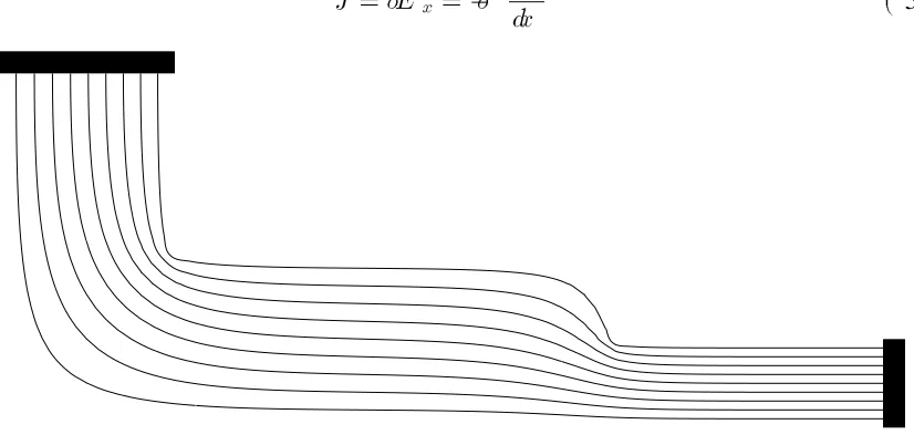
The fastest resistance extraction algorithms rely on the observation that the current flow in interconnect is usually one-dimensional. The field lines in Figure 3 demonstrate this property; near disturbances such as corners, junctions, and contacts, the current density distribution is complex, but in the long regions that form most of the pattern, it is uniform. In these straight sections, the Y and Z partial derivatives are 0, and Laplace’s equation is reduced to a 1-dimensional case. For the region depicted in Figure 4, the y and z components of ~
E are 0, as are those of the current density:
~
J =E
x =0
dV
dx
[image:18.612.125.538.309.510.2]( 5)
Figure 3: Current Distribution Near Disturbances
If we integrate this equation from v1 to 0 and from 0 to x1, we can derive a relation
between the current density and the voltage:
Z
0
v1
dV=0 Z
x1
0
J
x
dx ( 6)
v1= Z
x1
0
1
J
x
dx ( 7)
V1
0
x1
Figure 4: Uniform Current Region
Equation 2 is equal to this x component times the cross-sectional area, y1z1. Since
current is conserved, Jx is a constant:
R= v
i =
R
x1
0 1 J
x dx
R
S J
x dS
= x1 y1z1
( 8)
If a sheet resistance Rsh=1=( z1) is defined, then Equation 8 becomes the familiar
expression R=RshL=W, where Rshhas units of =2. Programs based on this
approxima-tion break a region into constituent rectangles, each of which contains connecting nodes formed by transistors, contacts and adjoining rectangles. The extractor then determines the dominant direction of current flow, sorts the nodes in this direction, and adds resistors between adjacent nodes in the list. Each resistor has a value R=Rsh( y20y1) =W, where ( y20y1) is the distance between the points in the direction of current flow and W is
the width of the rectangle.
be fairly accurate. If the net is highly irregular, or has an aspect ratio near unity (such as the well resistance in CMOS), the approximation will be fairly poor.
Most extractors designed for use on large designs are implementations of this algo-rithm. The simplest [37, 47, 53, 55, 61] simply calculate the resistance for each rectangle and assume that the overall result will be fairly accurate because these resistances are dominant. More sophisticated methods [3, 25] have empirically developed correction factors to compensate for corners, contacts, and other sources of field disturbance. The most sophisticated program using this method is McCormick’s EXCL[35], which only assumes one-dimensional flow in regions where it is certain to be valid. The values for the remaining sections of a net are either looked up in a library or solved using finite differences.
Both extractors described later in this chapter use the one-dimensional approxima-tion. The fast extractor described in the next section uses it exclusively, while the finite element extractor (Section 2.6) uses it selectively for sections where it is an accurate approximation.
2.3
Polygonal Decomposition Implementation
This section describes how the fast extractor, which is based on the one-dimensional approximation of the last section, is implemented. The resistance extractor is a component of the layout editor Magic. The next subsection provides a brief overview of Magic’s underlying database, including discussion of the opportunities that the database affords and some of the challenges that it presents to resistance extraction. Following this is a description of the modifications the extractor makes to the layout representation and a description of the algorithm’s core.
2.3.1
An Overview of Magic’s Database
rule checking, hierarchical circuit extraction, and plowing. A more detailed description of these and other features can be found in the 1984 Design Automation Conference Proceedings[44]. This section will concentrate on another Magic innovation: its novel database design.
The basic Magic data structure is the tile. The entire design area (Figure 5), extending to infinity, is covered by a mosaic of these tiles. Each point in the plane is covered by exactly one tile. Tiles may represent part of the design, as do the shaded ones in the example, or they may represent space. There are many possible configurations of rectangles that could be used to cover a region; Magic represents areas composed of a single material as a set of horizontal strips. In the example, the shaded region is broken into four tiles, t2, t4, t7, and t9. This representation prevents fragmentation of the region into many small rectangles and provides a canonical form for the design.
t0
t1 t2 t3 t4 t5
t6
t7 t8
t9 t10
[image:21.612.108.469.365.604.2]t11
Figure 5: A Plane of Magic Tiles
Corner stitches are used to represent the interrelation between tiles. A stitch is a
bottom tile along the left edge, and one to the leftmost tile along the bottom edge. Each tile’s corner stitches and the neighbors to which they point are shown as arrows in the example. These four stitches make local searching very fast. For example, all the neighbors of a given tile can be found by following stitches; in the figure, the top neighbors of tile t7 can be found by first following its right top pointer, then by following the bottom left pointers of the neighbors until the right edge of a neighbor is less than the left edge of the original tile. Similar algorithms exist for locating a point on the plane, searching for tiles in a given area, and visiting each tile in a region[45].
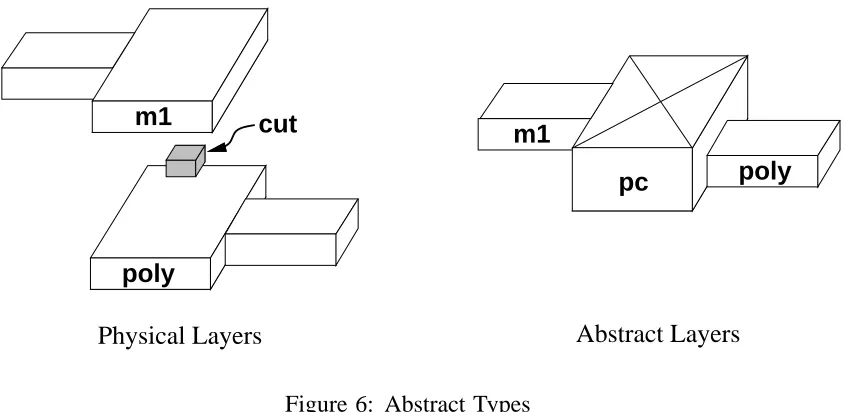
The remaining problem is developing a correspondence between the tile types of the database and the physical mask layers of a fabrication process. This problem is technology dependent; the designer must set up this correspondence for each fabrication technology used. One approach would be to use a separate tile type for each possible combination of overlapping layers, but this mapping would require an exponential number of types and would fragment the database into many small pieces. Another possible solution would be to use a separate tile plane for each mask layer. This solution requires fewer types (only one per mask layer), but is still memory inefficient because there are many more space tiles. This arrangement also lessens the advantages of corner stitching. Many layout operations involve more than one layer; calculating the interactions between such tiles is more difficult when they do not lie in the same plane.
Most technology mappings adopt an approach somewhere between the two described above. All layers that commonly interact with one another are placed in the same plane, while layers that do not are placed in separate ones. For example, the standard MOSIS SCMOS technology uses five planes: well, active, metal1, metal2, and oxide. As can be guessed from their names, the well, metal1, and metal2 planes contain types representing the wells and the two layers of metal used in the design. The oxide plane contains the locations of cuts in the chip’s passivation layer. The active plane contains the diffusion and polysilicon masks, plus combinations of these layers, such as transistors. These layers are put in the same plane because they closely interact. Interactions between layers on different planes is much rarer; for example, few operations need to know the relative spacings of polysilicon and metal.
than one of the above planes, such as contacts. This is done using special abstract tiles that have separate copies on both planes. For example, in Figure 6, the polysilicon, contact cut, and metal1 masks are combined to form the single abstract type pc. Duplicate copies of the pc tiles are kept on both the active and metal1 planes. These abstract types facilitate analysis of the layout because mask interactions need not be calculated explicitly; they are implied by the composite type.
m1
poly
pc
m1
poly
cut
Physical Layers
Abstract Layers
[image:23.612.84.506.254.460.2]pc
Figure 6: Abstract Types
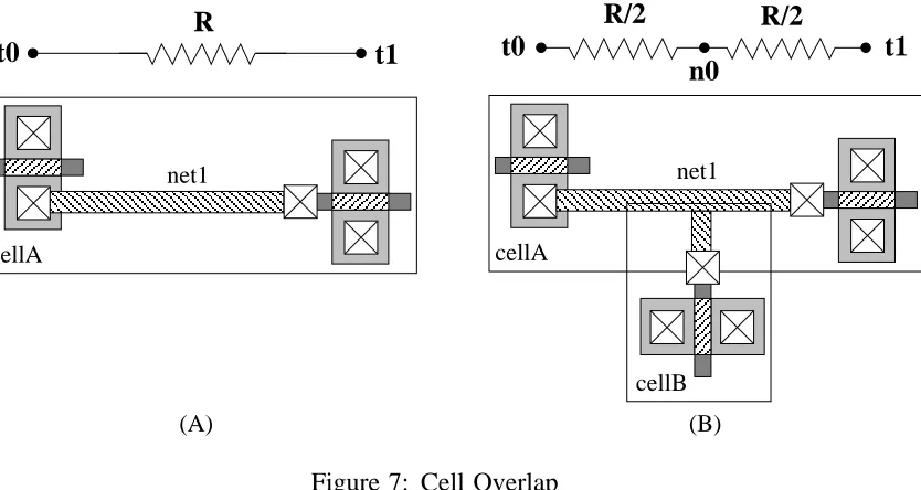
A cell is thus represented as a set of planes, each composed of tiles of varying types. Each cell can also contain subcells; interactions between these subcells present special problems. Magic allows nearly arbitrary overlap between cells; the only limitations are that cells must be individually design-rule correct and that overlap must not create or destroy devices. Any tools developed for the system must operate correctly regardless of the cell topology. Magic’s regular circuit extractor [52] is both hierarchical and in-cremental. To handle overlap, it extracts each cell individually, then flattens areas of cell interaction, extracts them and adjusts the connectivity and capacitance information accordingly. Because each cell is extracted independently of its context, only a cell and all its ancestors must be re-extracted when it is modified.
In the example of Figure 7a, the extraction of net1 in cellA produces a single resistor connecting the two transistors. When a second cell, cellB, is added over cellA, its metal line is shorted to the middle of net1. The initial version of net1 has no node at this point; the network for cellA would have to be split to create the required connection point. Allowing arbitrary overlap thus precludes context free extraction of cells.
cellA cellA
cellB
(A) (B)
net1 net1
t0
R
t1
t0
n0
t1
[image:24.612.127.544.232.454.2]R/2
R/2
Figure 7: Cell Overlap
It might be possible to devise a modified hierarchical system that allows network modification and back annotation to handle cases where cell overlap changes a network’s topology, but doing so would eliminate much of the advantage yielded by hierarchical extraction and would make the extractor much more complex. Instead, the resistance extractor copies and flattens all the electrically connected rectangles into a dummy cell. Despite the overhead of this approach, the extractor is still fast enough to run on an entire design, as will be seen in Section 2.7.
2.3.2
Database Preprocessing
Contact Removal
Magic’s contact types present problems for the extractor. Resistance extraction operates primarily on regions composed of a single mask layer. Abstract contact types tend to fracture this single layer into multiple pieces, as shown in Figure 8a. This artificial fragmentation makes extraction more difficult because it hides a region’s true topology. To avoid this, the extractor notes the position of each contact and then replaces it with its constituent mask layers (Figure 8b). This reduces the number of tiles and makes the inherent structure of the region more explicit.
poly
poly
poly
pc poly poly
(A) (B)
Figure 8: Dissolving Contacts
Region Coalescence
Another source of artificial region fragmentation is Magic’s use of of maximum horizon-tal strips (Figure 9a). This representation splits long horizonhorizon-tal regions between several rectangles. Since the one dimensional approximation is most accurate when the con-ducting edges of the region are perpendicular to the current flow, these areas need to be reshaped.
the corner is greater than its height. If it is (Figure 9b), then each tile in the region is split vertically at the corner. Once the tiles have been split, the extractor checks to see if they can be combined with their vertical neighbors (Figure 9c). Corners whose region height is greater than their width are likewise split and merged horizontally. Performing this operation at all concave corners produces the region of merged rectangles shown in Figure 9d.
20
λ
2λ
(A) (B)
(C) (D)
Figure 9: Modifying Horizontal Strips
original choices bad good
Figure 10: Interacting Concave Corners
2.3.3
Resistance Calculation
Once the database has been preprocessed, a resistance network is formed tile by tile. The user specifies a set of initial tile(s) that form the root of the power distribution tree, generally the power pads, which are put into a pending tile list. Tiles are processed one by one until none remain in the list. Each tile is processed in eight steps:
1. Check to see if this tile forms the gate or emitter of a transistor. If it does, add a node at the center of the tile, and set the corresponding device terminal equal to it.
2. Walk along the tile’s edges looking for electrically connected materials. For each connecting tile found, add a node at the center of the junction between tile edges. If the other tile has not already been processed, add it to the pending list.
3. If this tile type can form the source/drain or base terminal of a device, search the tile edges for transistor tiles. For each one found, add a node at the center of the common edge and set the correct terminal equal to it.
4. If this tile type forms the collector of a bipolar device, search under the tile on the emitter’s home plane for transistors. For each one found, add a node in the center of the emitter tile and set the collector terminal equal to it.
6. Calculate the minimum and maximum X and Y coordinates of all the nodes found in the previous steps. If max( X) 0min( X) >max( Y) 0min( Y) , assume that current
flows horizontally. If not, assume current flows vertically.
7. Sort the nodes from minimum to maximum in the direction of current flow. Merge nodes with the same coordinate.
8. Add a resistor between each adjacent pair of rectangles.
R= 8
<
:
Rsh1Y=width( tile) if current flow is vertical
Rsh1X=height( tile) if current flow is horizontal
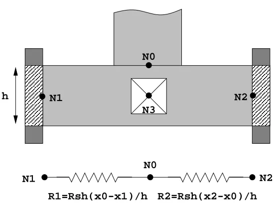
A simple example is shown in Figure 11. The extractor creates node N0 when it
finds the adjoining tile during the perimeter walk of Step 2. Nodes N1 and N2 are
created during Step 3 because the tile forms the source terminal of two transistors. Node
N3 is created during Step 5 for the contact contained within the rectangle. Since the
greatest horizontal separation (between nodes N1 and N2) is greater than the maximum
vertical separation (between nodes N0 and N3), the extractor assumes that current flows
horizontally. The nodes are sorted by x coordinate; since Nodes N0 and N3 have the
same value, they are merged. Two resistors, R1 and R2, are created between the node pairs, N1 0N 0 and N00N 2, and are added to the overall network description. The
extractor marks this tile as processed and goes on to the next one in the pending list. When all the tiles associated with a node have been processed, the resistors and transistors connecting to the node are examined. Resistors with both terminals connected to the node are eliminated. The extractor tries to combine any resistors in parallel connecting to the node. If there are no transistors and only one resistor connected to the node, the node and its connecting resistor are eliminated. Nodes with two connecting resistors and no transistors are also removed, and their resistors are combined.
N1
N0
N3
N2
N0
N1 N2
R2=Rsh(x2-x0)/h R1=Rsh(x0-x1)/h
[image:29.612.132.407.113.317.2]h
Figure 11: Extraction Example
2.4
Finite Differences
The one dimensional approximation is extremely efficient, since is is basically a scan through the list of tiles. For irregular shapes, however, it can produce a poor estimate of the resistance. Two other approaches, finite differences and finite elements, are often used when greater accuracy is needed. This section describes finite differences, which are simple to implement and adequate for some problems, while the next section describes the more powerful (and complicated) finite element method.
If the Taylor Series for the voltage is expanded around the point( x;y) , it can be used
to estimate the values at ( x+1x;y) and ( x01x;y) .
V( x+1x;y) =V( x;y) +1x @V
@x
+1x
2@
2
V
@x
2 +1x
3@
3
V
@x
3 +111 ( 9)
V( x01x;y) =V( x;y) 01x @V
@x
+1x
2@
2
V
@x
2 01x
3@
3
V
@x
3 +111 ( 10)
If these two equations are added, all the odd powers of1x cancel out. By rearranging
@
2
V
@x
2
V( x+1x;y) +V( x01x;y) 02V( x;y) 1x
2 ( 11)
An analogous equation for @
2
V=@y
2 can be derived in the same way. When these
two equations are added, the result is an approximation for Laplace’s equation in two dimensions: @ 2 V @x 2 + @ 2 V @y 2
V( x+1x;y) +V( x01x;y) 02V( x;y) 1x
2 +
V( x;y+1y) +V( x;y01y) 02V( x;y) 1y
2
= 0 (12)
Rearranging Equation 12 gives an approximation for V( x;y) in terms of its four
neighbors, V( x01x;y) ,V( x+1x;y) , V( x;y01y) , and V( x;y+1y) .
V( x;y) 1y
2
( V( x+1x;y) +V( x01x;y) )
21x
2
+21y
2 +
1x
2
( V( x;y+1y) +V( x;y01y) )
21x
2
+21y
2
( 13)
If the region is covered with a rectilinear mesh, as shown in Figure 12, then the voltage distribution can be calculated by solving the system of linear equations relating the mesh node potentials to one another. In this derivation, the distances between mesh points in a given direction (1x and 1y are constants), but an equivalent expression for
a nonuniform node distribution may be derived in the same manner; the only difference is that Equation 10 must be scaled by the ratio of the mesh spacings so that the first derivative terms will still cancel one another[22].
While Equation 13 is clearly true for points in the interior of the mesh, it must be modified for points along the boundary. For points on a conducting edge, the potential is fixed at V
c, the edge’s potential. For points along an insulating edge, the boundary
condition requires than the normal current be 0. This can be achieved by mirroring the voltage about the edge:
V( x;y) =
21y
2
V(x+1x;y)+1x
2
(V(x;y+1y) +V(x;y01 y))
21x
2
+21y
Figure 12: Finite Difference Mesh
V( x;y) =
21y
2
V(x01x;y)+1x
2
(V(x;y+1y) +V(x;y01 y))
21x
2
+21y
2 rightedge ( 15)
V( x;y) = 1y
2
(V(x+1x;y)+V(x01x;y))+21x
2
V(x;y+1 y)
21x
2
+21y
2 bottomedge ( 16)
V( x;y) = 1y
2
(V(x+1x;y)+V(x01x;y))+21x
2
V(x;y01y)
21x
2
+21y
2 topedge ( 17)
For convex corners, the voltage is mirrored in both directions.
These equations give the potential for discrete points in the region; the next step is to convert this system of equations into a corresponding resistance network. Surprisingly, a resistance network can be produced without explicitly calculating all the voltages interior to the region. The next two sections describe an efficient method for performing the conversion: the finite difference grid is represented as a mesh of resistors, which can be transformed directly into the desired resistor network.
2.4.1
Physical Analogs of Finite Differences
Gx
Gx
Gy
Gy
V(x+1,y) V(x,y+1) V(x-1,y) V(x,y-1) V(x,y)Figure 13: Lumped Analog of Finite Difference Equations
V( x;y) = G
X
V( x+1x;y) +G
X
V( x01x;y) +G
Y
V( x;y+1y) +G
Y
V( x;y01y)
2G X
+2G Y
( 18)
This equation is very similar to Equation 13; if Gx 1y
2 and G y1x
2, then the
two are identical. The solution is not unique, however; any values of Gxand Gythat have
the same ratio Gy=Gx=1x
2
=1y
2 will produce the same voltage distribution. With this
in mind, we can pick conductance values that also produce the correct current distribution. Equations 19 and 20 give the discrete approximations for the current density.
J
x =E
x
V( x+1x;y) 0V( x;y)
1x
( 19)
J
y =E
x
V( x;y+1y) 0V( x;y)
1y
( 20)
If1x and1y are small, then Jxand Jywill be essentially constant across the rectangle
and the integral of Equation 2 will just be the current density times the cross-sectional area. For a region of thickness t:
I
x
t( 1y) J
x =
t1y
1x
( V( x+1x;y) 0V( x;y) ) ( 21)
G
x =t
1y
1x
I
y
t( 1x) J
y =
1y
( V( x;y+1y) 0V( x;y) ) ( 23)
G
y =t
1x
1 y
( 24)
The values of G x and
G
y have the correct ratio, 1x
2
=1y
2. These analogs provide
an intuitive feeling understanding of finite difference analysis. A region is broken into a set of small rectangles, each of which is replaced by a simplified resistor network. This network can then be solved and replaced by an equivalent network that does not contain the interior portion of the mesh.
2.4.2
Solving the Equations
Once the equations have been formulated and modified to account for the various bound-ary conditions, the resulting system must be solved. Any algorithm for solving sparse, positive definite matrices may be used here, including Successive Overrelaxation (Section 5.5.2) and Cholesky Decomposition (Section 5.5.1), but significant performance advan-tages can be obtained by using the node elimination approach of Harbour and Drake[22]. As noted in the previous section, a finite difference formulation produces a mesh of lumped resistors, as does the entire extractor; instead of applying a test voltage to each boundary in succession, node elimination simply transforms the finite difference network into the desired network. To do this, the conductance matrix is first partitioned into two sections: one containing the set of nodes e that are to be retained and the other the set
of nodes ithat are to be removed.
G= 2 4 G ee G ei G ie G ii 3 5 2 4 V e V i 3 5 = 2 4 I e I i 3 5
( 25)
Since there is no current injected into the internal nodes, I i
= 0, and the equations
can be rewritten and solved forV e: G ee V e +G ei V i =I e
( 26)
G ie V e +G ii V i
Rearranging Equation 27 and substituting it into 26 gives an equation forV
e alone:
V
i =0G
01 ii
G
ie V
e
( 28)
( G
ee 0G
ei G
01 ii
G
ie ) V
e =I
e
( 29)
The term in parenthesis in Equation 29 is an equivalent conductance matrix G0
ee that
relates the boundary nodes and voltages without calculating the internal values; it is the same matrix that would be produced by applying a test voltage to each edge in turn and measuring the currents flowing to all the other edges. The conductance matrix for the entire system could be constructed using this equation, but inverting G
ii would be very
expensive because it is nearly as large as G. Instead, Equation 29 can be applied to
individual nodes as they are created.
G1
G2
G3 G4 N1
N2
N3 N4
N1
N2
N3 N4
G1G2/GT
G2G3/GT
G3G4/GT
G1G4/GT
G1G3/GT
G2G4/GT
GT=G1+G2+G3+G4 N0
[image:34.612.118.545.374.632.2](A)
(B)
Figure 14: Node Elimination
Consider a node N0 that connects to n other nodes, shown in Figure 14a for n =4.
This node can be eliminated by applying Equation 29. The inverse matrix G01
ii is the
the row and column vectors containing the values of G1111Gn. Multiplying these terms
gives the value for a new resistor Gij in terms of the old ones.
G
ij
( ne w ) =G
ij
( ol d) + G0
i G0
j
G
T
( 30)
G
T =
n
X
k =1 G
k
( 31)
Once all the resistor analog elements connecting to an internal point have been cal-culated, this formula can be applied to eliminate the node. Internal nodes can thus be eliminated as they are created; if the order in which nodes are processed is chosen care-fully, this algorithm will be considerably faster and will use less memory than would creating the entire matrix and then solving it. Section 2.6 describes an implementation of this algorithm.
2.5
Finite Elements
The finite difference approximation is adequate for regions without much variation in width and current density. When the current density does change considerably, main-taining acceptable accuracy is difficult due to the rectilinear grid; using small enough elements to provide sufficient accuracy in complicated areas requires use of too many elements in simpler sections. Since power supply networks often contain large variations in width and current density, solving them using finite differences would be very expen-sive. A more general approach, the finite element method, can be used to circumvent this problem.
x
y
V
Original surface
x
y
V
[image:36.612.230.418.524.678.2]Finite Element Approximation
Figure 15: Approximation of a Potential Surface
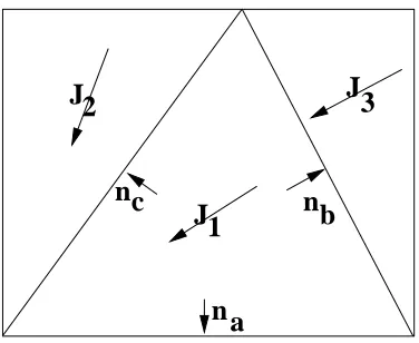
Since the potential in each element is fixed by the potentials at its vertices, the key is finding a set of equations that relate an element’s vertex potentials to one another and to those of neighboring elements. This is done by requiring the current flow between elements to be continuous; the current flowing out across each edge of one element must equal that flowing in across the same edge of its neighbor. For the center element in Example 16, this gives three equations:
nc
na
n
b
J1
J2
J
3
J11n a
=0 J11n
b
=J31n b
J11n c
=J21n c
By repeating this for all the patches adjoining a given vertex, the finite element approximation produces an equation defining the vertex’s potential in terms the values at adjoining vertices. When all the elements covering the region are processed, the result is a system relating the node potentials to one another; with the correct potentials applied at the conducting boundaries, the system will give an approximate solution to Laplace’s equation for the region. The accuracy will depend on how closely each patch lies to the actual surface. As patches get smaller, the surface regions they represent become more planar, and the solution accuracy improves. The same conclusion can be reached by considering the current densities; as patches get smaller, the current density of the surface region that they represent becomes more and more constant and approaches that of the patch. This suggests that the ideal mesh would have many small elements in places where the current density changes rapidly, and fewer, larger ones where the density is more uniform. Section 2.6 explores this problem in detail.
The finite element method can also be considered a generalization of the finite differ-ence method. The finite differdiffer-ence approximation requires that the first derivatives of the potential be continuous in both the X and Y directions. Using finite elements, the first derivative (in this case the gradient) must again be continuous, but the mesh does not have to be rectilinear and the derivative need not be independently continuous in both the X and Y directions.
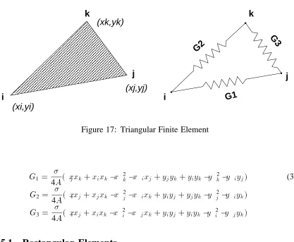
Like the finite difference method, relations between the vertex node potentials are often expressed in terms of a physically analogous resistor network to allow use of the node elimination technique described in the last section. Appendix A contains a detailed derivation of the analog for a triangular finite element; only the result is included here. The relation between the three vertices is represented as three conductors, with values given below. Ais the element’s area. A network for the entire system can be constructed
adjoin each edge.
i
j
k
(xi,yi)
(xj,yj)
(xk,yk)
i
k
j
G1
G2
G3
Figure 17: Triangular Finite Element
G1 = 4A ( x j x k +x i x k 0x 2 k 0x i x j +y j y k +y i y k 0y 2 k 0y i y j ) (32)
G2 = 4A ( x i x j +x j x k 0x 2 j 0x i x k +y i y j +y j y k 0y 2 j 0y i y k )
G3 = 4A ( x i x j +x i x k 0x 2 i 0x j x k +y i y j +y i y k 0y 2 i 0y j y k )
2.5.1
Rectangular Elements
Another commonly used element shape is the rectangle. The discrete conductors for a rectangular element (Figure 18) can be derived by considering it as two triangles. Solving the two elements i jk and i j
0
k and summing the two diagonal resistors gives values for
the five conductors.
G
j
= ( (1y0y 0) ) =( 21(0xx 0) ) G
k
= ( (1y0y 0) ) =( 21(0xx 0) ) G
l
= ( (1x0x 0) ) =(12(0yy0) ) G
m
= ( (1x0x 0) ) =(12(0yy0) ) G
n
= 0
i
j
k
j’
Gn
Gj
Gk
Gl
Gm
(X0,Y0)
(X1,Y1)
(X1,Y0)
(X0,Y1)
Figure 18: Rectangular Finite Element
As expected, these equations are similar to those of the finite difference analog in Section 2.4.1; the total conductance is the same, but in the finite element case, it is split between the two node-pairs along each edge instead of being assigned to a single one. For a uniform grid, each finite element node-pair not on a boundary will receive half an element of conductance, making the finite element and finite difference physical analogs identical. Finite difference analysis is thus a special case of finite element analysis with rectilinear elements.
2.5.2
Boundary Conditions
Satisfying the boundary conditions for finite element systems is simple. Insulating bound-aries conceptually can be treated as any other region, except that the conductance is 0.
Because of this, the discrete conductors all have 0 value and can be ignored. Perfectly conducting boundaries are regions for which =1, so the discrete conductors have
2.6
Finite Element Implementation
To check the accuracy of the simple one-dimensional extractor, Ariel also includes a finite element extractor. Since finite element analysis is slow, this second extractor will only perform it on subregions too complicated to extract by other means. Techniques described in the next two sections subdivide a region and identify the parts where detailed analysis is either unnecessary or redundant. These methods are based on similar components of the extractor EXCL[35]. Following this is a description of the finite element mesh generation and solution techniques used.
2.6.1
Region Subdivision
Finite difference and finite element analysis both produce resistors between each pair of nodes in a net, or ( N
2
0N) =2 elements in all. For a power bus, the number of nodes
is quite large because the region itself is large and has many connecting transistors. Producing a network for the entire region at once is not feasible; it would take too long to compute and would be too large to use. The region needs to be subdivided into smaller sections which can be extracted independently of one another.
The best way to do this is using the idea of breaklines developed by Horowitz [25] and extended by McCormick [35]. Breaklines are subdivisions added in long, straight parts of the region in such a way that the current distribution is not significantly dis-turbed. An example is shown in Figure 19. At the region’s corner, the lines of constant potential are unevenly spaced, but they become quite uniform a relatively short distance away. If the region is split parallel to these field lines, and the newly created regions are modelled as perfectly conducting boundaries, then the region’s field is virtually un-changed. McCormick calculated that splitting the region one square away from a source of disturbance only adds an error of about 0.1% in the calculated resistance.
Although adding a breakline increases the total number of nodes by 2, it makes two smaller problems out of the original large one. When breaklines are added next to all long, straight sections, the large region is divided into many small ones.
Figure 19: Adding Breaklines to Regions
(A)
(B)
(C)
Figure 20: Implementing Region Subdivision
A
B
C
D
E
F
G
H
Figure 21: Possible Rotations of a Region
2.6.2
Subregion Library
The extra region fracturing performed in the previous section produced two classes of rectangles: those with uniform current flow and those with nonuniform flow. For the former, resistance calculation is trivial; from Section 2.2, R=RshL= W. The latter require
further calculation. The resistance for each nonuniform rectangle cannot be calculated by itself; it must be considered along with its neighbors. Each group of adjoining non-uniform tiles form a cluster, which is bounded by space tiles, modelled as insulating edges, and by transistors, contacts, and uniform-flow rectangles, which are modelled as perfectly conducting edges.
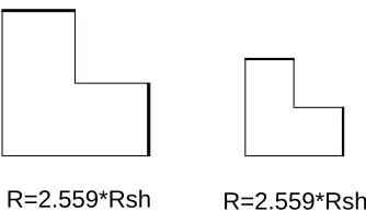
R=2.559*Rsh R=2.559*Rsh Figure 22: Region Scale Invariance
Since cells are often rotated or flipped, it is important that the clusters match regardless of rotation. Figure 21 shows the 8 possible rotations of an asymmetric cluster. There are a number of ways to make entries match regardless of rotation. One approach would be to make an additional key for each unique rotation of the cluster. The advantage of this is that table accesses are fast; no additional processing must be done to a cluster before it is compared against the library keys. The primary disadvantage is that it uses additional memory; since the key for an entry is often as large as the entry itself, and most large clusters are asymmetric, such a library would be prohibitively large. Instead, a single canonical key is used. The extractor first calculates the centroid of each region, then rotates the region so that the center of gravity is as low and as far to the left as possible. In the example, rotation F would be chosen. This scheme usually only requires one key, making it memory efficient. It has two disadvantages: the library access time is greater due to the cost of calculating the centroid, and the rotation may not be unique if the centroid lies on the line x=y. In practice, the increased access time is unimportant
because extraction time is dominated by the finite element calculation itself. To ameliorate the second problem, the extractor calculates the centroid of the conducting edges if the correct rotation is ambiguous. (Since the edges are actually lines, they are first assigned a small finite width.) Sometimes, this will also fail to give a unique rotation. In this case, the region will actually get extracted more than once. The loss of efficiency due to unnecessary duplication of extraction is negligible, however; in practice, the large clusters whose processing dominates the extraction time have too many rectangles and edges to be ambiguous.
sizes, the two regions of Figure 22 have the same resistance. In his library implementa-tion, McCormick normalizes all rectangles to 1/256th of the first rectangle’s height. Such an implementation would not work for a power bus extractor due to the great variation in width. It is not uncommon for minimum width wires to connect to an extremely wide main power bus. Any rounding in the width of these minimum width wires due to quantization could introduce substantial error in the overall resistance.
Another scaling implementation might be possible, but its utility in the power network domain is questionable. The large, multirectangle regions that dominate the extraction time are not scaled versions of other regions, and any time spent providing scale inde-pendence is wasted for them. Since the potential return for scaling is problematical, the extractor does not use it.
2.6.3
Mesh Generation
The extractor must produce a network for any cluster that does not match an entry in the library. McCormick and Horowitz both use finite difference analysis when they need to accurately extract a region; unfortunately, this approach proves inadequate for power bus extraction. Power buses have a wide variations in width; a rectilinear grid that provides adequate accuracy near small features will run too slowly in the large, coarse sections of the design.
To accommodate large feature size variation, some sort of nonuniform finite element mesh generation is needed. One possible approach is the adaptive mesh generation algorithm devised by Machek and Selberherr[34]. This method has two drawbacks for resistance extraction. First, it requires that the internal node voltages be calculated; the fastest solution algorithm for resistive meshes, node elimination (Section 2.4.2), does not calculate these intermediate values. Use of adaptive mesh generation would require the one of the slower solution techniques be used. The other problem is that the mesh would have to be regenerated for each edge; since the potential distribution varies depending on the boundary to which the voltage is applied, the mesh will also vary.
1
4 2
5 3
A
E
C D
B
[image:45.612.98.470.166.375.2]F
Figure 23: Sources of Potential Disturbance
[31] is instead used. The basic idea of this algorithm is to produce a mesh with many el-ements in places where the current density is changing rapidly and fewer in places where it is changing slowly. To do this, the region is first represented as a set of rectangular elements1 containing regions of homogeneous resistivity. Each of these elements
adjoin-ing a point of voltage disturbance needs to be subdivided. The disturbances are caused by concave corners in the regions. In the example of Figure 23, the disturbances are the bend in the region (labelled 1) and the corners around the contact (labelled 2-5). Kemp also uses the entire edge between two regions of differing resistivity (labelled A-F), but this seems unnecessary; as can be seen from the potential lines, the current does not change rapidly except at the corners.
Each element adjoining a disturbance is recursively split in two until the elements nearest the corner are below some minimum size. The basic idea in splitting is to subdivide the element in such a way that the resulting children are well ratioed,2 and to
1The initial elements are rectangles because Magic’s database only supports orthogonal shapes.
Al-though Kemp’s algorithm can handle arbitrary shapes, the current discussion is limited to the Manhattan case.
(a)
(b)
(c)
(d)
(e)
Figure 24: Subdivision of Elements
minimize the number of nodes required by making the split points of adjacent elements align. The following rules (illustrated in Figure 24) are applied:
Ill-ratioed rectangles are split in two along their long side.
a. If there is an edge between two elements along one side, and
subdividing there does not give children more ill-ratioed than the parent, split the element at the edge. If there is more than one such edge, use the one that gives the best ratioed children.
b. If there is no such edge, split the element in the middle.
Well-ratioed rectangles can be split in either direction.
c. Split at the adjacent edge that gives the best ratioed children.
d. If no such edges exist, split along a line perpendicular to the
expected direction of current flow.
e. For a corner element with no adjacent edges, split in both
directions.
Once the adjacent element is subdivided, the same procedure is applied to all of its children that are next to the disturbance. This continues until all of the adjacent elements are smaller than some predefined size. Figure 25 shows how this algorithm operates on a concave corner. The edges are numbered in the order in which they were added, with the letter (a-e) in parentheses showing which rule was applied.
Triangularization Grid Generation
1(e)
2(e)
3(b)
4(c)
5(d)
6(a)
7(b)
8(c)
9(b)
10(c)
11(b)
[image:47.612.78.496.111.337.2](A)
(B)
Figure 25: A Mesh Generation Example
This algorithm works reasonably well. Elements end up being fairly square; such regions generally have less current density variation than does a long, thin one. Requiring mesh lines to match up reduces the total number of elements. Splitting in two makes the element density spread out in about a 45 degree line from the disturbance, just as the change in current density does. The mesh generator thus puts many elements where they are necessary and fewer where they are not.
Once the elements have reached the desired size, they are replaced by a finite element mesh. Element vertices and edges form the nodes and edges of the mesh, respectively. The mesh is composed of two element types: rectangles and triangles (Figure 26). The triangles always occur in groups of three that form a rectangle. The extractor decides which element to use depending on the number of neighbors the element has. Elements with four neighbors use the rectangle, while those with five use the three triangle set. Some of the elements may have more than five neighbors; this is fixed by splitting them along one of the edges to form two elements. Figure 25 shows the mesh elements added during triangularization.
Rectangular Triangular Figure 26: Finite Elements Used in Generation
so that they can be represented as a tile) are copied into a dummy cell. Solution accuracy can be controlled using an optional scale factor by which all rectangles are magnified as they are copied. A large scale factor results in smaller final elements near a disturbance. The cluster is then searched for concave corners. At each such corner, the horizontal tile is split along the y-axis at the corner to produce the three initial rectangles of Figure 25, each of which is then processed by the above algorithm. The algorithm is done when the corner’s adjacent elements are all 1 by 1 squares. The extractor then makes a second pass through the entire cluster, looking for elements with more than five neighbors. Each such element is subdivided again, and the adjacent elements are rechecked to insure that the additional edge does not leave them with too many neighbors. The final triangular-ization is not explicitly performed because Magic can only represent rectangles. Instead, the extractor adds the elements for all three triangles at once whenever a five-neighbor rectangle is encountered.
2.6.4
System Solution
1 2 3 4
5 6 7 8
9 10 11 12
13 14 15 16
17 18 19 20
21 22 23 24
a b c d e
f g h i j
k l m n o
p q r s t
u v w x y
a b c
d e f g
h i j
1 2
3 4
5
6 7
8
[image:49.612.94.469.106.333.2](A)
(B)
Figure 27: Order of Node Elimination
By processing the elements in short rows, the number of outstanding nodes (nodes that have some but not all of their connecting resistors in place) is kept low. The numbers in Figure 27a show the order in which elements are processed, while the letters indicate the order in which nodes are eliminated. For rectangles that are wider than they are tall, elements are processed by column instead of by row.
Implementation of this algorithm is trickier when is grid is not rectilinear. There are two interrelated problems: choosing an order of element processing that will minimize outstanding nodes and determining when all the resistors connecting to a node have been processed. For regions that are taller than they are wide, the extractor uses Magic’s tile enumeration algorithm. This algorithm visits tiles in the top to bottom, left to right order of their lower left corners. The example of Figure 27b shows this ordering. At each tile, the extractor generates the correct mesh elements, then marks the tile as processed. It then checks the nodes along the sides of the tile to see if all their adjoining tiles have also been processed.3 If they have, then the node is eliminated. For rectangles that are
3It is not really necessary to check all four edges; another method would be to automatically process