F E B R U A R Y 1 9 8 9
WRL
Research Report 89/2
Optimal Group
Distribution in
Carry-Skip Adders
The Western Research Laboratory (WRL) is a computer systems research group that was founded by Digital Equipment Corporation in 1982. Our focus is computer science research relevant to the design and application of high performance scientific computers. We test our ideas by designing, building, and using real systems. The systems we build are research prototypes; they are not intended to become products.
There is a second research laboratory located in Palo Alto, the Systems Research Cen-ter (SRC). Other Digital research groups are located in Paris (PRL) and in Cambridge, Massachusetts (CRL).
Our research is directed towards mainstream high-performance computer systems. Our prototypes are intended to foreshadow the future computing environments used by many Digital customers. The long-term goal of WRL is to aid and accelerate the development of high-performance uni- and multi-processors. The research projects within WRL will address various aspects of high-performance computing.
We believe that significant advances in computer systems do not come from any single technological advance. Technologies, both hardware and software, do not all advance at the same pace. System design is the art of composing systems which use each level of technology in an appropriate balance. A major advance in overall system performance will require reexamination of all aspects of the system.
We do work in the design, fabrication and packaging of hardware; language processing and scaling issues in system software design; and the exploration of new applications areas that are opening up with the advent of higher performance systems. Researchers at WRL cooperate closely and move freely among the various levels of system design. This allows us to explore a wide range of tradeoffs to meet system goals.
We publish the results of our work in a variety of journals, conferences, research reports, and technical notes. This document is a research report. Research reports are normally accounts of completed research and may include material from earlier technical notes. We use technical notes for rapid distribution of technical material; usually this represents research in progress.
Research reports and technical notes may be ordered from us. You may mail your order to:
Technical Report Distribution
DEC Western Research Laboratory, UCO-4 100 Hamilton Avenue
Palo Alto, California 94301 USA
Reports and notes may also be ordered by electronic mail. Use one of the following addresses:
Digital E-net: DECWRL::WRL-TECHREPORTS
DARPA Internet: [email protected]
CSnet: [email protected]
UUCP: decwrl!wrl-techreports
Optimal group distribution in carry-skip adders
Silvio Turrini
Copyright
1989
Digital Equipment Corporation
Abstract
1. Introduction
The addition of two binary numbers A and B can be obtained by means of the relations :
C0 = 0
Si = Ai xor Bi xor Ci [ Sum ]
Ci+1 = Gi or ( Pi and Ci ) [ Carry into bit i+1 ]
where
Pi = Ai xor Bi [ Propagate signal ]
Gi = Ai and Bi [ Generate signal ]
and
i = bit position starting with the LSB of the adder
In a simple carry-ripple adder the worst case delay is proportional to its size, because if a carry is generated in the LSB it will ripple through the entire structure.
If we divide the total number of bits into groups, the following rules apply to each group : •If each Ai # Bi in a group, then we do not need to compute the new value of Ci+1 for that
block; the carry-in of the block can be propagated directly to the next block.
•If Ai = Bi = 1 for some i in the group, a carry is generated which may be propagated up to the output of that group.
•If Ai = Bi = 0, a carry, will not be propagated by that bit location.
The basic idea of a carry-skip adder is to detect if in each group all Ai # Bi and enable the block’s carry-in to skip the block when this happens. In general a block-skip delay can be different from the delay due to the propagation of a carry to the next bit position.
In the case of a one-level skip adder, we need to generate for each group a signal Skip1, which is simply the logic and of all Pi in that block. Skip1 will enable the skip cell to propagate the group’s carry-in directly to the input of the next group.
Skip1 = Pn and Pn-1 and ... and P1
n = number of bits in the group
The total adder delay will be the worst case carry propagation delay plus the delay of producing the last
Sum bit.
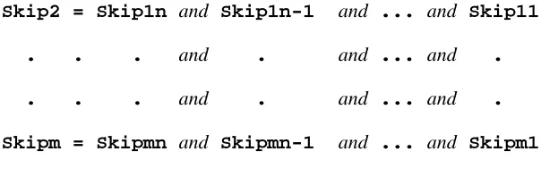
Skip2 = Skip1n and Skip1n-1 and ... and Skip11
. . . and . and ... and .
. . . and . and ... and .
Skipm = Skipmn and Skipmn-1 and ... and Skipm1
where Skipij is the jth signal at level i
Many papers on the choice of skip groups have been written, but all of them treat the problem without considering some important details. They restrict it, sometimes implicitly, to a particular implementation and to the simpler cases, such as a one or two level carry-skip adders. In the paper by Lehman and Burla [2] the best configuration is found for groups of equal size; Majerski [5] also studied the problem, and Guyot, Hochet and Muller [3] reduced the optimal group distribution to the solution of a geometrical problem. In the paper by Oklobdzija [6] and Barnes [1] a method is described to determine the optimum division of a carry chain. Examples for one and two levels of carry-skip are also described, but the method cannot be applied if the delays of the different cells do not satisfy certain limitations. The algorithm proposed here overcomes the following limitations of previous methods :
•Asymmetric distributions can also be generated. Some of the papers, such as [3], consider only symmetric distributions.
•The possibility of a carry-in to the low order bit of the adder is taken into account, allowing efficient performance of two’s complement arithmetic.
•Different delays can be assigned to the ripple cells and to the skip cells at each level of carry-skip. No matter which technology we consider, the node at the end of a block, where two or more carry paths merge, has a higher capacitance than the intermediate nodes in the carry chain. This means that the delay associated with the cells driving that node is higher in technologies such as CMOS, where gates must be resized to optimize performance, or in technologies such as ECL, the power must be increased due to the different electrical situa-tion.
•There is no limitation on the number of carry-skip levels. It is possible to improve adder performance by using three or more skip-levels. For example in CMOS, extending the num-ber of carry-skip levels to three and even four has small cost in terms of area and can lower the total adder delay by one or two gate delays in the case of a 32-bit data path. The application of this methodology to ECL yields an adder that is not only very efficient in terms of silicon area and current consumption, but the total delay also can be very low and comparable to the most complex and expensive adders such as carry-look ahead adders, conditional sum adders and Ling adders [4].
•Cells which propagate the carry faster than necessary are identified so that the excess speed can be eliminated or taken into account during the optimization process. This is very useful in ECL where the delay of a gate is a function of the power dissipated by that gate.
2. Worst case carry delay
Let us define the order of a carry-skip adder as the number of levels of its carry-skip circuitry and a
block as any distribution of bits of the adder grouped together and bypassed by a skip cell. A block also
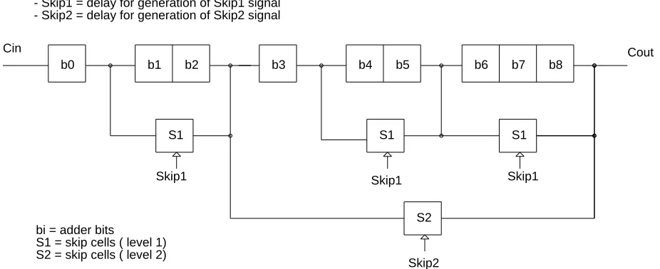
[image:6.612.106.408.70.169.2]Depending on the operands provided there are many carry paths with different propagation delays. We are interested in the longest of them, because it will be the worst case carry propagation delay of the adder. In general the worst case path is composed of three basic subpaths :
•A carry is generated in some block and propagates to the output of that block in a time proportional to the size of the block. Let us call this delay Dg.
•From the output of the block where it has been generated, the carry skips a certain number of other blocks with a total delay Ds.
•Finally it ends in a block after rippling through a certain number of bits with a delay De, which is proportional to the size of the block. Because we are interested in the worst case delay only the slowest carry path will be considered.
The total worst case delay, Dt will be the sum of the three Di :
Dt = Dg + Ds + De
In the example of Figure 1 a possible worst case path could be :
b1 ---> b2 ---> b3 ---> S1 ---> b6 ---> b7 ---> b8
where a carry is generated in b1 and propagates up to b8 through ripple ( bi ) and skip ( Si ) cells.
But it could be :
b0 --> S1 --> b3 ---> S1 ---> b6 ---> b7 ---> b8
if the delay in S1 is higher than the sum of the ripple delays through b1 and b2.
In order to design the optimum adder, the right distribution of blocks as well as their internal arrange-ment which minimizes this time, must be found for all possible combinations of inputs.
b0 b1 b2 b3 b4 b5 b6 b7 b8
Cin Cout
Skip1 Skip1 Skip1
Skip2
S1 S1 S1
S2 Delays :
- all bi have the same ripple delay
- S1, S2 delay for propagating carry through skip cell - Skip1 = delay for generation of Skip1 signal - Skip2 = delay for generation of Skip2 signal
bi = adder bits
[image:7.612.91.554.473.662.2]S1 = skip cells ( level 1) S2 = skip cells ( level 2)
To find an algorithm which, given the number of bits of the adder and the associated delays of all the different cells, optimizes the distribution, is a hard problem. It is even harder if we want to overcome the simplifying assumption that the delays in all the possible carry paths are the same.
The problem is simplified if instead of providing the adder’s number of bits and finding the optimal distribution with the associated worst case carry delay, we provide the total worst case carry delay and we find the optimal distribution for that delay with the associated total number of bits. By varying the provided worst case delay, the algorithm will generate optimal distributions which will be characterized by a different number of bits. The one with a total number of bits equal to or larger than the value requested by the design will be chosen. We will start this process with a minimum delay, which is the one required for just a single group at the assigned carry-skip level to operate correctly, and we will proceed until the appropriate distribution is generated.
In general we might obtain distributions which will not necessarily have the usual number of bits found in adders ( 16, 32, 64 etc.), but might be higher. This simply means that for the given worst case carry delay, the number we obtain represents the maximum number of bits that can fit the optimal distribution generated. We can eliminate some configurations of bits in order to obtain the desired number, without affecting the worst case delay. The elimination can be done according to some simple rules that will be given later.
3. Basic observations on the algorithm
The basic idea is to assign to each of the adder’s blocks of bits a pair of delays corresponding to a carry generation and a carry ending in that block. The delay will be function of the block’s position along the carry path. Each block, according to the constraints imposed by the assigned delays, will contain a maximum number of bits. The combination of the delays introduced by all the blocks will be equal to the given maximum carry propagation delay allowed to the adder.
Starting with a given worst case carry delay for the adder, we will divide it into time intervals accord-ing to the position of the block along the carry path, and we will generate the combination with the maximum number of bits. During the generation process, which we will call expansion of the block, the way that bits will be grouped together will be a function of the carry-skip level assigned to the block, or
order of the block. If we are dealing with a 0-order block we can generate the maximum possible number
of bits directly. If the order is higher we can consider the block as if it were a lower order carry-skip adder itself and we can recursively apply the same procedure to the block. So, for a given a carry-skip level higher than the trivial case of zero, the algorithm will generate a tree whose nodes correspond to blocks and whose levels correspond to carry-skip levels. The leaves of this tree will be the bits of the adder, and the roots are the blocks generated by the division of the total adder delay into time intervals during the initial phase. The tree structure will respect the rule that from a parent block only the most prolific descendents will be generated. These are those which will be able to generate the largest number of bits. The paths which connect the roots to the largest number of leaves will form the final optimal distribution.
block depending on its position along the carry path. As we proceed along the carry path going through blocks, the first number in the delay pair i will increase, because more time will be allowed in the case of a carry generation, while the second number , j , will decrease by the same amount, because a carry which enters the block has a delay which increases as we get closer to the carry out of the adder. We also want to use profitably the time spent in the generation of the highest level Skip signal by using this time in generating blocks at a lower level where the corresponding Skip signals are ready. So the initial part of the list of blocks will include some lower-order blocks to take care of this.
4. General algorithm
The algorithm can be logically divided into two steps :
•Partitioning and delay assignment. Starting with the total carry delay, the set of constraints at the highest level will be computed and assigned to corresponding blocks.
•Building the tree. The whole tree will be generated, starting with the initial constraint assign-ments and working down to the lowest level. The paths which connect the blocks generated in the previous step to the largest possible number of bits that can be generated from them will define the optimal structure.
4.1. Partitioning and delay assignment
In this section and in the rest of the paper, we assume that a carry propagates from left to right : the leftmost bit is the adder’s LSB. The partitioning and the assignment of the delays to each block is a two-step process :
1st step : At any carry skip level desired, the basic rule which determines the block generation is that the delay associated with a carry generation will be the same as the delay that a carry would have if it skipped that block. For the first block the situation is slightly different, because the Skip signal must be ready before we can profitably use the skip circuitry. The delay associated with carries that end in the block is simply the dif-ference between the total carry delay and the delay at the output of the previous block.
2nd step : In the second step we will compute other delay pairs of decreasing level, starting from the delays associated with the first block generated in the first step, down to the minimum possible delay of a carry generated in a single bit. The i value in the delay pair is computed by adding the maximum of the Gi and Pi delay to the delay of the skip cell at that level. The change from the partitions generated at the first step is that the new ones will have a lower carry-skip level. As said before, the lower level is because the corresponding Skip signal is already set and the proper skip-circuitry can be used.
4.2. Building the tree
The final list will be visited and action taken according to the value of the skip-level of the partition :
D <= min(di, dj)
where
D = max total group delay for a carry generation or kill
di = max delay when a carry is generated in the block
dj = max delay for a carry to ripple in the block before being killed
For example assume that the delay associated with Pi and Gi signals is one unit delay. Then for the delay pair {3,4} we can generate two bits, because in this case the first number in the pair, that is three, is the tighter constraint on the maximum number of bits that satisfies the relation above. In fact it takes :
1 ( for Pi ) + 2 ( for rippling ) = 3 unit delays
for a carry to be generated and to ripple through the two bits. Now assume the delay pair {4,2} and the same assumptions about the delays. Then both values would have limited to three the total number of bits that can be generated from this partition. This is because it takes :
1 ( for Pi ) + 3 ( for rippling ) = 4 unit delays
for a carry to be generated in the first bit and to ripple through the 3 bits, but only 2 units for entering the block and rippling up to the next to last bit.
If skip level >= 0 : This algorithm can be recursively applied to a new list of partitions one level lower, which is generated from the given delay pair. Only the partition which will generate the largest number of bits will be chosen as the best candidate. With the list of possible partitions are associated delays which vary from the given delay to the min-imum possible amount, that is the delay of just one bit. During this evaluation delays between subsequent blocks will differ by the delay of a skip cell one level down. For example, if we assumed for simplicity that the delays of all the cells involved at all levels were equal to 1 unit delay and we started with {4,5} at level 2, the possible choices would be :
{2,5} {3,4} {4,3} set of 3 elements
{3,5} {4,4} set of 2 elements
{4,5} the original partition
The value two in the carry generation delay has been established considering that the delay associated with the carry propagation of just one bit is :
delay of Pi + delay of rippling = 1 + 1 = 2
strategies are possible. In the program developed the set with the lower number of elements is chosen. This is because that partition will generate a smaller number of bits or groups of bits. This means that the fan-in of the gates involved in the Skip signals’ generation will be lower.
Printing groups When all the original partitions have generated the entire tree the process will stop and the whole structure, specifying the organization of the bits at each level, is printed.
This has been a general description of the algorithm with no differentiation among delays which belong to partitions at different places and levels along the list of possible candidates. In actual situations the delays, which correspond to a bit or group at the end of a list can be higher to take care of the different electrical situation where the different paths merge. The same applies to the delays of the skip cells. These differences can be taken into account without changing the basic behavior of the algorithm.
During the process of finding the optimal distribution with the required total number of bits, we provide increasing worst case carry delays which generate larger and larger final distributions. The increment that is added to the worst case carry delay at each step must be such that the new set of delay pairs will generate distributions with at least one more bit in them. This increment, called adder
ef-ficiency incremental delay, or AEID, is defined as the minimum incremental delay which, if added to the
worst case carry propagation delay, would generate a new distribution with at least one more bit.
One observation about the efficiency of this algorithm is that it has an exponential behavior when building the tree. However in practical cases, up to 5 or 6 levels and 128 bits, its performance is very good.
4.3. An example
As an example let us consider a 2-level 32-bit carry-skip adder, where the carry ripple delay, Gi and Pi signal delays, skip cell delays and the delays associated with all the Skip signals are all equal to a unit delay. Because we want a two-level carry-skip adder, we have to generate the signals Skip1 and Skip2. Here is a table that shows the delays associated with each signal, starting from time zero.
signal total delay
Gi, Pi 1
Skip1 2
Skip2 3
and it takes 1 unit delay to skip a block at both levels
For representing the delays and the level, we will used the notation {i,j,k} , where i and j will represent the delays associated with the carry generation and carry ending, while k will represent the level of the partition. Assuming we start with a total adder delay of 8, the first list will be :
{4,5,2} {5,4,2} {6,3,2} {7,2,2} {8,1,2}
The value 5 in the first triple represents the maximum allowed delay for carries that end in this block. It is computed considering that the carry coming from the previous block, which will be part of the list generated at the second step, must have a delay which will differ by one skip cell delay from the 4 value, i.e. one unit. This is because we always want the delays in the carry-ripple and carry-skip paths be the same to maximize the number of bits in each partition. So if we subtract from the total adder delay of eight the value generated by the previous block, that is three, we obtain five units.
The other values are generated considering that at each step along the list, i is increased by one carry skip delay at that level and j must decrease by the same amount, because as we proceed along the list, one more skip cell is added. At the second step we will add new partitions at a lower level and the new list will be :
{2,8,0} {3,6,1} {4,5,2} {5,4,2} {6,3,2} {7,2,2} {8,1,2}
The value of two in the first block is the minimum carry delay generated assuming that the minimum block size is one. In this case the delay is equal to two units because we have one delay unit for Gi or Pi and one delay unit for the carry to ripple through one bit. The maximum carry kill delay is equal to the given worst case carry propagation delay.
In the second block, i is equal to three units and j is computed by subtracting the maximum delay at the output of the previous block from the total carry delay, that is :
8 - 2 = 6 units and k = 1
Now we have to visit each group of the list and either calculate the maximum number of bits, or generate a new list of delays for a lower level partition and apply the algorithm recursively. For the first group there is no choice since we can only generate a single bit. For the second partition, we can have the two possibilities :
1 2 or 2
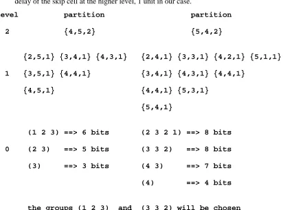
which represent two groups of one and two bits respectively with a skip cell at level 1 bypassing each group, or a single group of two bits with no bypass circuitry. Clearly the first choice generates more bits and therefore it will be selected as the best candidate. The same criteria can be applied to the rest of the list and the table in Figure 3 shows the expansion of two of the groups of the list. Each row displays the sets which can be generated starting from the given partition at the highest level, down to level zero. The groups which generate the largest number of bits will be chosen.
[image:12.612.55.514.601.655.2]The best distribution, which satisfies the requirements with 34 bits, is shown in Figure 2.
Figure 2: A 2-level 34-bit carry-skip adder
•The total number of bits exceeds by two bits the required adder size. The location of the bits to be eliminated can be based on ease of implementation, such as lowering the maximum fan-in of the gates or lowering the carry-skip level of some block. In our example the maximum fan-in is three and will not change by the elimination of only two bits, because there are six groups of three bits. If the last bit in the last group is eliminated however, we can eliminate a 2-level carry bypass. The location for the elimination of the second bit is arbitrary. In this example the last bit in the next to last group has been chosen. So one possible 32-bit distribution is the one shown in the Figure 4.
•Eliminating some bits does not change the worst case carry propagation delay unless the elimination lowers both delays associated with the block to which the bits belong. As will be clarified in the next section, if a test on the total number of bits generated is included in the algorithm and at each step the right AEID is always provided, by construction the previous generated distribution must have had a number of bits smaller than the one requested. In our example it can easily be proved that the AEID is constant at each step and is equal to the delay of the skip cell at the higher level, 1 unit in our case.
level partition partition
2 {4,5,2} {5,4,2}
{2,5,1} {3,4,1} {4,3,1} {2,4,1} {3,3,1} {4,2,1} {5,1,1}
1 {3,5,1} {4,4,1} {3,4,1} {4,3,1} {4,4,1}
{4,5,1} {4,4,1} {5,3,1}
{5,4,1}
(1 2 3) ==> 6 bits (2 3 2 1) ==> 8 bits
0 (2 3) ==> 5 bits (3 3 2) ==> 8 bits
(3) ==> 3 bits (4 3) ==> 7 bits
(4) ==> 4 bits
[image:13.612.96.508.250.556.2]the groups (1 2 3) and (3 3 2) will be chosen
Figure 3: Expansion of 2 partitions
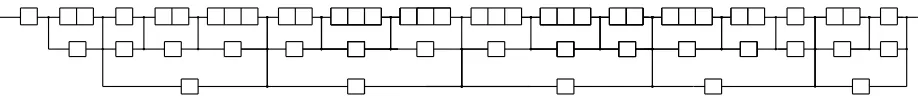
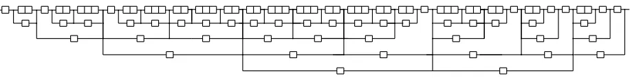
[image:13.612.90.551.635.690.2]Figure 5 shows another example, a 4-level 56-bit carry-skip adder with the same assumptions about the cells’ delays as in the 32-bit example. In the diagram shown, the carry’s worst case delay is 8 gate delays, the same as in the previous example.
Figure 5: A 4-level 56-bit carry-skip adder
4.4. Enhancements : AEID and control of the delay of each bit
As defined in section 2, the AEID is the minimum delay that the worst case carry propagation delay must be incremented by, in order to generate a new distribution with at least one more bit. This assures that in the process of determining the distribution with the right number of bits, there will always be a perfect matching between number of bits and the worst case carry propagation delay that they generate and no excess time will be wasted in some bit or group of bits. The AEID is implemented very simply. Every time a block is generated we compare the delay that this block will actually generate with the limits defined by the delay pair. The difference is compared with the previous AEID and saved if it is smaller. Also, the difference between the actual delay and the maximum allowed for the configuration can be saved with the node representing the partition. In this way we can keep track of the excess performance of some bits and adjust the speed of the cells involved by lowering the power, in the case of an ECL implementation, or resizing the gates in the path, in the case of a CMOS design.
5. An ECL 32-bit carry-skip adder implementation
During the adder development at WRL speed was not the only concern; its area and power consump-tion were even more important. This is because WRL is interested in VLSI applicaconsump-tions where an adder is only a very small part of the chip. With a 2-level carry-skip adder, all the requirements have been fulfilled.
The process used is good in achieving circuit density, but bad for the transistor performance and can be roughly characterized by :
•The process is double poly.
•3 um emitter minimum npn transistor.
•3 metal layers, but 1 dedicated totally to power supply. •4 um pitch for interconnection metal layers.
•Transistor performance, characterized by aτfof 35 ps.
From the layout and spice simulations, the results are :
•Area of 0.3 x 2.1 mm, voltage reference generators included. •Worst case adder delay of about 1.7 ns.
•Power consumption of about 0.6 Watts using a power supply voltage of -5.2 V.
Figure 6 shows a partial layout of the adder.
The speed of this adder is comparable to the speed achievable with more complex implementations. The reason why this adder is so fast, although its total delay is 8 gate delays + the delay of the last xor operation, compared to 3 gate delays for a Ling adder, is because the gate delay in the two implemen-tations is very different. In the Ling adder, the loading conditions and the total number of gates limit the speed of each gate. In a Ling adder almost all the gates are in the critical path and all must be powered up to increase the performance of the adder. In the carry-skip adder the number of gates is lower compared to a Ling adder by a factor of at least 3 and the load at each gate is very low. Moreover, only a few gates need to be powered up in order to improve the overall performance.
Thus the power consumption is many times lower in the carry-skip case for comparable performance. Finally, the area of a Ling adder is so large that it is difficult to imagine VLSI applications, such as single-chip CPUs or FPUs, where it would be appropriate.
Spice simulations at WRL also indicate that with better transistor performance and slightly higher power consumption ( still under a Watt ) a sub-nanosecond delay is achievable.
adder/Sum P Ci S GND vee2 vr3vee1vr2GND1vregve adder/Sum
P Ci
S GND vee2 vr3vee1vr2GND1vregve adder/Sum
P Ci
S GND vee2 vr3vee1vr2GND1vregve adder/Sum
P Ci
S GND vee2 vr3vee1vr2GND1vregve adder/Sum
P Ci
S GND vee2 vr3vee1vr2GND1vregve adder/Sum
P Ci
S GND vee2 vr3vee1vr2GND1vregve
skip2
Rc2 Rc0
GNDvr3vee1vr2Bi
Rc1 skip1b Ci2 vreg skip Pib vee2 GNDc Ci0
adder/or3GNDvee1 GND1vr2 ve
Cexor a
a skip1 vr3vr2 vreg
s P Pi Ci1 C vee GNDc Bi GNDvee1 a a
adder/or32vr2P2bGNDvr3vee1 GND1vregve Cexor adder/genreg vr3vr2 vee1 vee2Cexor adder/ripple2 ve vreg vr2 vr3vee1 vee2Pi GND BicGND1
Cexor adder/ripplevr3vee1vr2 vregve vee2PiGND BicGND1
Cexor adder/or2
vee GND1vreg GNDvr3vee1vr2 adder/genreg
vr3vr2 vee1 vee2Cexor
adder/ripplevr3vee1vr2 vregve vee2PiGND BicGND1
Cexor adder/ripplevr3vee1vr2 vregve vee2Pi GND BicGND1
Cexor
adder/Pigen vr2 vr3vee1 vregve vee2AiBiGND BicGND1
P Pi
adder/Pigen vr2 vr3vee1 vregve vee2AiBiGND BicGND1
P Pi
adder/Pigen vr2 vr3vee1 vregve vee2AiBiGND BicGND1
P Pi
adder/Pigen vr2 vr3vee1 vregve vee2AiBiGND BicGND1
P Pi
adder/Pigen vr2 vr3vee1 vregve vee2AiBiGND BicGND1
P Pi
adder/Pigen vr2 vr3vee1 vregve vee2AiBiGND BicGND1
P Pi adder/group2 P9 C8 P8b C7 P7b P6bC6 P5bC5 C4 P4b adder/Sum P Ci S GND vee2 vr3vee1vr2GND1vregve adder/Sum
P Ci
S GND vee2 vr3vee1vr2GND1vregve adder/Sum
P Ci
S GND vee2 vr3vee1vr2GND1vregve
a skip1 vr3vr2 vreg
s P Pi Ci1 C vee GNDc Bi GNDvee1 a a adder/or2 vee GND1vreg GNDvr3vee1vr2 adder/ripplevr3vee1vr2 vregve vee2PiGND BicGND1
Cexor adder/ripplevr3vee1vr2 vregve vee2PiGND BicGND1
Cexor
adder/Pigen vr2 vr3vee1 vregve vee2AiBiGND BicGND1
P Pi
adder/Pigen vr2 vr3vee1 vregve vee2AiBiGND BicGND1
P Pi
adder/Pigen vr2 vr3vee1 vregve vee2AiBiGND BicGND1
P Pi adder/group1 C3 C2 P2b C1 P3b P1b C0 adder/figure
6. Conclusion
We have introduced a new technique for designing fast and efficient multi-level carry-skip adders. The program developed at WRL, which implements this algorithm, generates the optimal distribution in less than a second of VAX 785 CPU time, even for configurations with 128 bits and 4 or more carry-skip levels. It also computes additional information regarding the delay of each individual bit and the group partition of the adder. This is very helpful during the process of adjusting the power in ECL designs, or in comparing design trade-offs during the process of sizing the gates in MOS implementations. Our experience with a real design has proved that carry-skip adders are very fast and efficient.
7. Acknowledgements
References
[1] Barnes Earl R. and Oklobdzija Vojin G.
New Multilevel Scheme for Fast Carry-Skip Addition.
IBM Technical Disclosure Bulletin 27(11), April, 1985.
[2] Lehman M., Burla N.
Skip techniques for high-speed carry propagation in binary arithmetic units.
IRE Transaction on Electronic Computers , December, 1961.
[3] Guyot Alain, Hochet Bertrand, and Muller Jean-Michel. A Way to Build Efficient Carry-Skip Adders.
IEEE Transactions on Computers C-36(10):1144-1151, October, 1987.
[4] Ling H.
High-speed binary adder.
IBM Journal of Research and Development 25, May, 1981.
[5] Majerski S.
On determination of optimal distribution of carry skips in adders.
IEEE Transactions on Computers EC-16, February, 1967.
[6] Oklobdzija Vojin G. and Barnes Earl R.
Some optimal schemes for ALU implementation in VLSI technology.