Realization of Asynchronous Null Convention
Logic circuits using Mapping Algorithm
Ms. Shraddha Bhardwaj Prof. Riyaj Kazi
PG Student Assistant Professor
Department of Electronics & Telecommunication Engineering Department of Electronics & Telecommunication Engineering Dr. D.Y. Patil School of Engineering,Pune Dr. D.Y. Patil School of Engineering,Pune
Abstract
Designs with higher performances, more complexity and shrinking feature size increases the prevalence of asynchronous design paradigms in the multi-billion dollar semiconductor industry. The automation techniques therefore become a challenge in the application areas of asynchronous circuits. In this paper a new methodology is suggested which is used for mapping multi-rail logic expressions to NCL Gate Library. This methodology is then compared to a method which already exists. These methods are implemented in VHDL programming language. The outcome is increased performance in terms of delay and area.
Keywords: Automation, Gate Mapping, NULL Convention Logic, Technology Mapping
________________________________________________________________________________________________________
I.
INTRODUCTION
NULL Convention Logic is an asynchronous design paradigm [1-7].It offers the best opportunity for integrating the asynchronous digital design into predominantly synchronous semiconductor design industry .NCL systems have power, noise, and EMI advantages compared to synchronous circuits, performance and design reuse advantages compared to synchronous and non–DI asynchronous paradigms, area and performance advantages for designing complex systems , like SoCs, including substantially reduced crosstalk between analog and digital circuits, integrating multi-rate circuits effortlessly, and facilitation of component reuse and technology migration.
The main reason for not applying asynchronous design paradigms, such as NCL in industry is the absence of standard Computer Aided Designs (CAD) tools that assist in automating the design process. Technology Mapping is the core of such design flows since the performance of such mapped circuits is directly proportional to its efficiency. In this paper, a mapping algorithm is proposed whose performance is enhanced than other existing design methods.
Overview of NCL: A.
NCL circuits are comprised of 27 fundamental gates, in which the set of all functions consists of four or less variables. Since each rail of an NCL signal is considered as a separate variable, a four variable function is not same as a function of four literals which is made up of eight variables. The primary type of threshold gate is the THmn gates having n inputs, when m of the n inputs are asserted then the output becomes asserted. In a THmn gate, each of the n inputs is connected to the rounded portion of the gate; the output emanates from the pointed end of the gate; and the gate’s threshold value, m, is written within the gate as shown in fig 1
Fig. 1: Thmn Threshold Gate
A dual-rail signal, D consists of two mutually exclusive wires named as D0 and D1, which assumes any value from the set {Data 0, Data1, Null, Invalid} as shown in table I
Realization of Asynchronous Null Convention Logic circuits using Mapping Algorithm (IJSTE/ Volume 1 / Issue 11 / 085)
NCL threshold gates are designed with hysteresis state-holding capability, so that for the output to be asserted, all inputs must be deasserted before the output will be deasserted. Hysteresis makes complete transition of inputs back to NULL before asserting the output of the next wave front of input data. That is why a THmn gate is equivalent to an n-input C-element.
II.
METHODOLOGY
Mostly all asynchronous NCL designed circuits should satisfy the criteria of Input Completeness and Observability. The design flow of NCL takes care of the issues related to synthesis of synchronous register-transfer Level (RTL) design into an NCL netlist satisfying the Input Completeness and Observability criteria and optimization of NCL circuits under the cost function of area and delay.
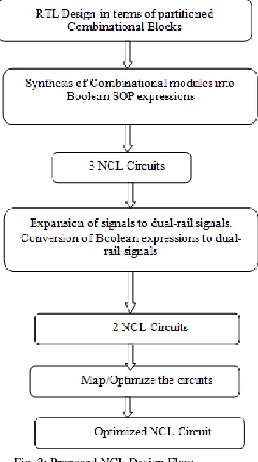
The design flow used here starts with an RTL design written in VHDL and the RTL design specifies location of registers. The registers are replaced with NCL registers. RTL design is then partitioned in terms of combinational blocks.
Fig. 2: Proposed NCL Design Flow
In the next step, the modules are synthesized into Boolean SOP expressions which express its output in terms of its input. 3NCL circuits consist of SOP expressions. The Boolean expressions are then converted into dual-rail signals. The result is 2NCL containing dual-rail SOP expressions. The 2NCL circuits are then optimized and mapped to obtain a robust NCL Circuit.
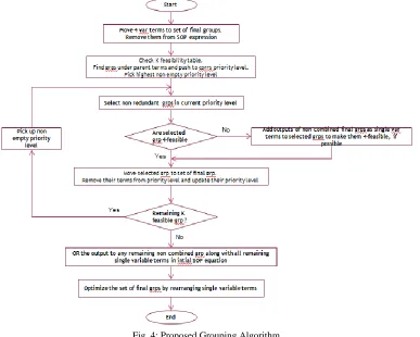
Original Mapping Algorithm: A.
Fig. 3: Original Grouping Algorithm
Proposed Mapping Algorithm: B.
Realization of Asynchronous Null Convention Logic circuits using Mapping Algorithm (IJSTE/ Volume 1 / Issue 11 / 085)
III.
RESULT
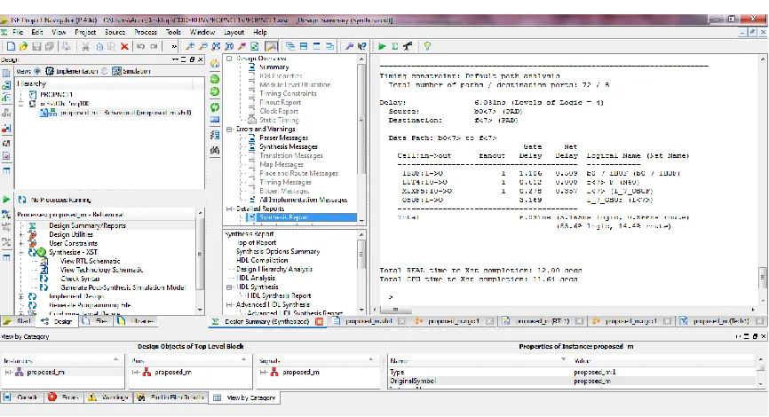
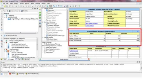
The result is obtained after VHDL implementation of original mapping algorithm and proposed mapping algorithm. The delay and area is obtained after comparing both the outputs. The screen shots of the same are shown in Figures below. The delay obtained by Original Mapping Algorithm is above method is 6.725ns.
Fig. 5: Delay obtained by Original Mapping Algorithm
Fig. 6: Delay obtained by Proposed Mapping Algorithm
Fig. 7: Area obtained by Original Mapping Algorithm
Fig. 8: Area obtained by Proposed Mapping Algorithm
IV.
CONCLUSION
Realization of Asynchronous Null Convention Logic circuits using Mapping Algorithm (IJSTE/ Volume 1 / Issue 11 / 085)
REFERENCES
[1] Farhad A. Parsan, Waleed K. Al-Assadi and Scott C. Smith, ―Gate Mapping Automation for Asynchronous NULL Convention Logic Circuits,‖ IEEE TRANSACTIONS ON VERY LARGE SCALE INTEGRATION (VLSI) SYSTEMS, VOL. 22, NO. 1, JANUARY 2014
[2] K. M. Fant and S. A. Brandt, ―NULL convention logic: A complete and consistent logic for asynchronous digital circuit synthesis,‖ in Proc. Int. Conf. Appl. Specific Syst., Archit. Process., Aug. 1996, pp. 261–273.
[3] K. M. Fant, Logically Determined Design: Clockless System Design with NULL Convention Logic. New York: Wiley, 2005.
[4] S. C. Smith and J. Di, ―Designing asynchronous circuits using NULL convention logic (NCL),‖ in Synthesis Lectures on Digital Circuits and Systems. San Mateo, CA: Morgan & Claypool, 2009.
[5] M. Ligthart, K. Fant, R. Smith, A. Taubin, and A. Kondratyev, ―Asynchronous design using commercial HDL synthesis tools,‖ in Proc. 6th Int. Symp. Adv. Res. Asynchron. Circuits Syst., Apr. 2000, pp. 114–125.
[6] C. Jeong and S. M. Nowick, ―Technology mapping and cell merger for asynchronous threshold networks,‖ IEEE Trans. Comput.-Aided Design Integr. Circuits Syst., vol. 27, no. 4, pp. 659–672, Apr. 2008.
[7] B. Bhaskaran, ―Automated synthesis and cycle reduction optimization for asynchronous NULL convention circuits using industry-standard CAD tools,‖ Ph.D. dissertation, Dept. Comp. Eng., Univ. Missouri - Rolla, Rolla, 2007.
[8] R. Reese, S. C. Smith, and M. A. Thornton, ―Uncle—an RTL approach to asynchronous design,‖ in Proc. 18th IEEE Int. Symp. Adv. Res. Asynchron. Circuits Syst., May 2012, pp. 65–72.
[9] J. McCardle and D. Chester, ―Measuring an asynchronous processor’s power and noise,‖ in Proc. Synopsys Users Group Conf., 2001, pp. 66–70.
[10] S. C. Smith, R. F. DeMara, J. S. Yuan, D. Ferguson, and D. Lamb, ―Optimization of NULL convention self-timed circuits,‖ Integr. VLSI J., vol. 37, no. 3, pp. 135–165, Aug. 2004.
[11] T. Verhoeff, ―Delay-insensitive codes—an overview,‖ Distrib. Comput., vol. 3, no. 1, pp. 1–8, 1988.
[12] G. E. Sobelman and K. Fant, ―CMOS circuit design of threshold gates with hysteresis,‖ in Proc. IEEE Int. Symp. Circuits Syst., vol. 2. Jun. 1998, pp. 61– 64.
[13] C. L. Seitz, ―System timing,‖ in Introduction to VLSI Systems. Reading, MA: Addison-Wesley, 1980, pp. 218 262.
[14] A. Kondratyev, L. Neukom, O. Roig, A. Taubin, and K. Fant, ―Checking delay-insensitivity: 104 gates and beyond,‖ in Proc. 8th Int. Symp. Asynchron. Circuits Syst., Apr. 2002, pp. 149–157.