Power Efficient Dual Dynamic Node Flip Flop
with Embedded Logic by Adopting Pulse Control
Scheme
Thara Sebastian Aravindhan A
PG Student Assistant Professor
Department of Electronics & Communication Engineering Department of Electronics & Communication Engineering Saintgits College of Engineering Saintgits College of Engineering
Abstract
In this paper a low power conditionally pulse enhanced dual dynamic node flip flop design is presented. The proposed structure combines the merits of dual dynamic node and a pulse control scheme (PCS) named conditional pulse enhancement mechanism. It eliminates the large capacitance present in the precharge node of several conventional designs by following a split dynamic node structure to separately drive the output pull-up and pull-down transistors. The conditional pulse enhancement scheme consists of a simple pass transistor ‗AND‘ gate design and a pull up ‗pMOS‘. This set up reduces circuit complexity and removes the pulse generation control logic from the critical path, which facilitate a faster discharge operation as well as improvise the discharge speed conditionally. Various pre-layout simulation results based TSMC 180-nm technology reveal that the proposed design features the best power-delay-product performance compared to SDFF, HLFF, and DDFF. It also presents an area, power, and speed efficient method to incorporate complex logic functions into the flip flop. The performance improvements indicate that the proposed designs are well suited for modern high-performance designs where power dissipation and latching overhead are of major concern
Keywords: Conditional Pulse Enhancement, Dual Dynamic Node, Embedded Logic, Flip Flop (FF), Pass Transistor AND, Pulse Generation
________________________________________________________________________________________________________
I.
I
NTRODUCTIONTechnology and speed are always moving forward day by day, from low scale integration to large and VLSI and from megahertz (MHz) to gigahertz (GHz). The requirements are also rising up with this continuous advancing technology and speed of operation. In synchronous systems, high speed has been achieved using advanced pipelining techniques. Flip Flop (FF) is one o f the crucial elements used extensively in all kinds of pipelining techniques. It is estimated that a clock system and a logic part itself consume almost the same power in various chips. That is the clock system consumes 20–45% of the total chip power. The large power consumption of the clock system is due to large transition probability, while the transition probability of the ordinary logic is only one-third of the average. Within the clock system almost 90% of the total power is consumed by the FFs (T. Sakurai and T. Kuroda, 1996) As a result, reduced power consumption by the FF can have a huge impact on the total power consumption of system. In order to reduce the power of the clock system, the voltage swing of the clock should be reduced. Many methods are adopted to reduce the clock swing from earlier times itself (H. Kojima et.al., 1994) . But this method came with cost of four clock lines, which in turn increased area overhead and interconnection capacitance. Another reduced clock swing FF is introduced in (H. Kawugachi and T. Sakurai, 1998), using which the clock swing got reduced to 1V, which was a big achievement. Also from a performance perspective, the delay and latency of the FFs consumes a large portion of the cycle time, especially in high operating frequencies.
In this paper, chapter 2 gives a detailed description of the existing FF architectures and challenges in achieving high performance. Chapter 3 describes the proposed Conditionally Pulse Enhanced DDFF and its operations. It also explains about incorporating logic into the proposed FF. Section 4 presents the experimental results and findings are concluded in section 5.
II.
L
ITERATURE REVIEWConventional Flip Flops: A.
Large numbers of FFs and latches have been published in the past decades. They can be divided into static and dynamic design styles. Static FFs include the conventional master slave design. They dissipate comparatively low power and have a low clock to output (CLK – Q) delay. But the data to output delay (D-Q) is comparatively large in these FFs because of the large set up time. The second category of the FF design, the dynamic FFs includes the modern high performance FFs. There are purely dynamic designs as well as pseudo-dynamic structures. The latter, which has an internal precharge structure and a static output, deserves special attention because of their distinctive performance improvements. They are called the semi-dynamic or hybrid structures, because they consist of a dynamic frontend and a static output.
Static Flip Flops: B.
The Static FFs include the master slave designs, such as the transmission gate based master-slave flip-flop and the PowerPC 603 master-slave latch (S. Gari et al.,1994). They dissipate low power. But the D to Q delay is high because of their large setup time. PowerPC 603 was one of the most efficient classic static structures. It has the advantages of having a low-power keeper structure and a low latency direct path. As mentioned earlier, the large D to Q delay resulting from the positive setup time is one of the limitations of this design. Also, the large data and CLK node capacitances make the design inferior in performance. Despite all these shortcomings, static designs still remain as the low power solution when the speed is not a primary concern. In (G. Gerosa et al.,1994) they made use of this power efficient FF in 2.2V, 80MHz Superscalar RISC microprocessor.
Dynamic and Semi dynamic Flip Flops: C.
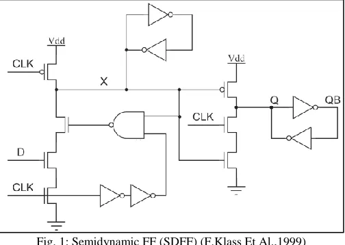
The dynamic FFs include the modern high performance FFs . There are purely dynamic designs as well as pseudo dynamic structures. Semidynamic FFs which has an internal precharge structure and a static output, deserves special attention because of their distinctive performance improvements. They consist of a dynamic frontend and a static output. SDFF is shown in Fig. 2.1 and HLFF is shown in Fig. 2.2. These FFs fall under semidynamic category. They benefit from the CLK overlap to perform the latching operation. SDFF is the
Fig. 1: Semidynamic FF (SDFF) (F.Klass Et Al.,1999)
Fig. 2: Hybrid Latch FF (HLFF) (H. Partovi Et Al.,1996)
The two major sources of power dissipation in the conventional semidynamic designs are the redundant data transitions and large precharge capacitance of the internal node. In order to reduce the redundant data transitions in the FFs many attempts have been made. The conditional discharge flip flop (CDFF) (P. Zhao et al., 2004) employs a technique named conditional discharge. In conditional discharge scheme an nMOS transistor controlled by output feedback is inserted in the discharge path of the stage with high-switching activity. This reduces overall power dissipation by eliminating unwanted transitions when a redundant event is predicted. As a result, transition at the output switch off the discharge path for first stage to prevent it from discharge and doing evaluation in succeeding cycles as long as the input is holds high. But the major disadvantage of this design is the additional nMOS in the transistor stack. This makes it slower and bulkier. The conditional data mapping FF (CDMFF) (C. K. Teh et al., 2006) is another such FF. This FF uses an efficient technique for reducing the redundant data transitions. It uses an output feedback structure to conditionally feed the data to the flip-flop. This reduces overall power dissipation by eliminating unwanted transitions when a redundant event is predicted. Since there are no added transistors in the pull-down nMOS stack, the speed performance is not greatly affected. But the presence of three stacked nMOS transistors at the output node, similar to HLFF, and the presence of conditional structures in the critical path increase the hold time requirement and D-Q delay of the flip-flop. Also, the additional transistors added for the conditional circuitry make the flip-flop bulky and cause an increase in power dissipation.
The next major reason for power dissipation is the large precharge capacitance in the conventional FFs. This is because in most of the conventional design a single internal node is driving the output transistors i.e. both pull up and pull down. These transistors in turn drive large output loads, which also contributes to the capacitance. This common drawback of many conventional designs was considered in the design of XCFF (A. Hirata et al.,2005). The power dissipation is reduced by splitting the dynamic node into two. Each node separately drives the output pull-up and pull-down transistors. Only one of the two dynamic nodes is switched during one CLK cycle. Therefor the total power consumption is considerably low in this FF without any reduction in speed. Major drawbacks of this design are the redundant precharges at internal nodes, requirement of large hold time because of the conditional shutoff mechanism and charge sharing at the internal node. Charge sharing occurs mainly in long discharge paths. When the transistors in the discharge path turns ON when the actual discharge is not needed a dip in the voltage of the internal nodes occurs. This is because of the junction capacitances of the turned ON transistors. This may degrade the voltage level and may cause erroneous transition at the output unless the inverter pair are carefully designed to overcome this. Embedding logic into the FF may result in uncontrollable charge sharing errors.
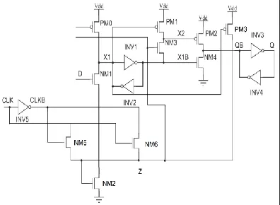
Another FF named Dual dynamic node pulsed hybrid flip flop (DDFF) (K. Absel et al.,2013) is shown in Fig. 2.3. In DDFF node X1 is pseudo-dynamic in nature. The weak inverter acts as the keeper here. The node X2 is purely dynamic unlike XCFF. Instead of the conditional shut OFF mechanism of discharge path in XCFF, this DDFF has an unconditional discharge path. The redundant precharge at nodes are also eliminated in this design. But the charge sharing problem exists here also. Node X1 undergoes charge sharing when the CLK makes a low to high transition while Dis held low. This results in a momentary fall in voltage at node X1. One of the major advantages of the DDFF is the ability to embed complex logic functions into the FF architecture efficiently. It is named as Dual dynamic node pulsed hybrid flip flop with Embedded Logic Module (DDFF-ELM) and is shown in Fig. 2.4. The fact that an N input function can be realized in a positive edge triggered structure using a pull-down network (PDN) consisting of Ntransistors improves the efficiency in terms of speed and area. The slight change in the clocking scheme makes the charge sharing problem in DDFF-ELM less, which become uncontrollable as the number of transistors increases. One limitation of this DDFF-ELM is the need of the large overlap period because of the long discharge path of internal node. This can be achieved by the use of bulky inverters.
Fig. 4: DDFF-ELM(K. Absel Et Al.,2013)
III.
A
NALYTICAL PROCEDUREProposed Flip Flop with Pulse Control Scheme: D.
results in reduced switching power at node Z. Also the discharging path contains reduced number of stacked transistors. As a result of this reduced number of transistors, the time to discharge the node X is less. I.e. the delay gets reduced.
In this design, the longest discharging path occurs when input data are 1. A transistor PM3 is added in order to enhance the discharge under this condition. Transistor PM3 is normally turned OFF because node X1 is HIGH most of the time. Only when node X1 is discharged to |VTP|, the transistor PM3 turns ON. This provides additional boost to node Z (from VDD-VTH to VDD). The generated pulse is taller, which enhances the pull-down strength of transistor NM2.
The voltage level of node X1 rises during precharge and turns off transistor PM3 eventually. A large pulse gets generated giving enough time to correctly capture the data only when it is needed. The bulky delay inverter in the DDFF and DDFF-ELM which consumes large power during pulse generation can be avoided. The leakage power also gets reduced because of the smaller transistors in the discharge path and in the delay inverter. Also the problems of charge sharing decreases as the number of transistors in the discharge path are less.
The working of Flip Flop is as follows. The latching of the data occurs only when the pulse is high. If the input is high prior to the pulse generation then node X1 is discharged through NM1-2 i.e. only through two transistors whereas it was three in case of DDFF resulting in a faster discharge. Also the generated pulse at this instant will be larger because node X1 turns ON transistor PM3 which pulls up the pulse to a strong ‗HIGH‘. This switches the state of the cross coupled inverter pair INV1-2. Causing node X1B to go high and output QB to discharge through NM4. The node X2 is held high by the pMOS transistor PM1. As the pulse falls low, the circuit enters the precharge phase and node X1 is pulled high through PM0, switching the state of INV1-2. During this period node X2 is not actively driven by any transistor, it stores the charge dynamically. The outputs at node QB and maintain their voltage levels through INV3-4. If D is zero prior to the pulse, node X1 remains high. The pulse generated during this time will have less voltage swing resulting in low power dissipation. Since X1 remains HIGH node X2 is pulled low through NM3 as the pulse goes high. Thus, node QB is charged high through PM2 and NM4 is held off. At the end of the evaluation phase, as the pulse falls low, node X1 remains high and X2 stores the charge dynamically. The architecture exhibits negative setup time since the short transparency period defined by the 1–1 overlap of CLK and CLKB, that is the pulse width allows the data to be sampled even after the rising edge of the CLK before CLKB falls low.
Embedded Logic Module: E.
Incorporating logic into FFs is somewhat difficult. SDFF is the capability to incorporate complex logic functions efficiently. By incorporating logic to the FF the area as well as delay can be reduced to a larger extent. The pipeline overhead of the whole circuit gets eliminated. Even though SDFF is capable of incorporating logic functions, the power consumed by this circuit is very large. In DDFF-ELM even though the charge sharing problem in SDFF is eliminated by the clock rearrangement, it requires a larger overlap period which is achieved by the use of bulky inverters. Charge sharing becomes uncontrollable as the number of transistors in the stack increases. For reducing this effect we have to decrease the number of transistors in the stack. By adopting conditional pulse enhancement mechanism we can achieve shorter discharge path as well as larger pulses only when the logic output needs to be HIGH.
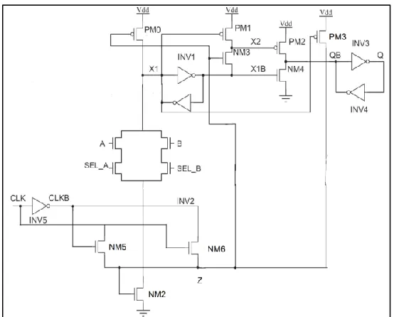
Fig. 3.2 shows the design of the proposed Conditionally Pulse Enhanced DDFF- ELM AND. A two input AND is embedded to the FF. The two inputs A and B get evaluated according to their values when the pulse is high. Here the longest discharge path consists of three transistors only and it occurs when A = B = 1 and pulse becomes high. Then the three transistors NM0-2 gets turned ON and PM3 pulls up the node Z and we get a sufficiently large pulse in order to latch the value of the logic to the output. In all other cases i.e. A = 0 and B = 1, A = 1 and B = 0, A = B = 0, PM3 remains OFF and we get pulses with low voltage swing resulting in less power dissipation.
Fig. 6: Proposed Conditionally Pulse Enhanced DDFF-ELM AND
Fig. 7: Proposed Conditionally Pulse Enhanced DDFF-ELM MUX
IV.
R
ESULTS AND DISCUSSIONIn order to understand the effectiveness of the proposed design, the performance of the proposed FF design is evaluated against the existing design. The compared designs include SDFF, HLFF, DDFF and DDFF-ELM. The Pyxis schematic of Mentor Graphics is used in order to create the schematics of the circuit. The performance of the pulse enhanced P-FF design is evaluated against existing designs through pre-layout simulations using eldo simulator. The output waveforms are viewed using E-Z wave viewer. The target technology is the TSMC 180-nm CMOS process. Since pulse width design is crucial to the correctness of data capture as well as the power consumption, the transistors of the pulse generator logic are sized for a design spec of 120 ps in pulse width. The operating condition used in simulations is 500 MHz/1.8V. In order to analyze the power consumption data pattern with 50% transition probability is given at a temperature of 27oC.
Output Waveform of Proposed FF: A.
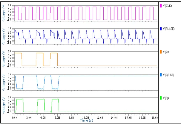
Fig. 8: Simulation Wave Form Of Proposed Conditionally Pulse Enhanced DDFF
Output Waveform of Proposed FFs with Embedded Logic Module: B.
Fig. 4.2 and Fig. 4.3 show the output waveform of Proposed Conditionally Pulse Enhanced DDFF-ELM AND and MUX. It is evident from the waveforms that only when the output needs a transition from ‗LOW‘ to ‗HIGH‘ an enhanced pulse gets generated. In all other cases pulses with low voltage swing are generated. In the case of ‗AND‘ logic only when both the inputs are ‗HIGH‘ we are getting an enhanced pulse. Similarly when select signal and input are high an enhanced pulse gets generated.
Fig. 4.2: Simulation Wave form of Proposed Conditionally Pulse Enhanced DDFF-ELM AND
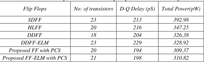
Table 4.1 illustrates the speed and power delay product (PDP) of various flip-flops at 50% data activity. The results show that the proposed flip-flops have the lowest power dissipation among the group. The transistor count remains almost same for all the flip flops. Also the D-Q delay is also less compared to other Flip Flops.
Table - 4.1
Performance Comparison Of Various Flip Flops At 50% Data Activity
Flip Flops No: of transistors D-Q Delay (pS) Total Power(pW)
SDFF 23 213 392.98
HLFF 20 216 347.25
DDFF 18 204 326.38
DDFF-ELM 23 229 328.92
Proposed FF with PCS 20 194 309.37
Proposed FF-ELM with PCS 21 198 310.82
The Table 4.2 gives a detailed comparison of DDFF to the proposed Conditionally Pulse Enhanced DDFF. The results show that the proposed flip flop gives 9.8%, 18.2%, and 18.7% reduction in Power Delay product (PDP) compared to DDFF, Embedded AND logic, and Embedded 2x1 MUX logic respectively. This shows that the power as well as the speed of the proposed FF is improved.
Table - 4.2
Performance comparison of DDFF and proposed FF
Logic Functions
DDFF Proposed FF
∆PDP Power Dissipated (pW) D to Q Delay (ns) Power Dissipated (pW) D to Q Delay (ns)
FF 326.38 0.204 309.37 0.194 9.8%
AND Logic 328.92 0.229 310.82 0.198 18.2%
2 x 1 MUX 344.44 0.230 315.38 0.204 18.7%
V.
C
ONCLUSIONThe clock system (FF modules) of a circuit consumes nearly half of the total power. Therefore reducing the power of clocking elements can reduce the total power consumption of the system. The choice of the flip flop design has a huge impact on the power consumption as well as performance of the system. Here, a Conditionally Pulse Enhanced DDFF is proposed. Proposed FF is capable of effectively incorporating logic to the FF also. The conditional pulse enhancement scheme consists of a simple two transistor pass transistor ‗AND‘ gate design. The conditional pulse enhancement scheme reduces the number of transistors stacked along the discharging path and it supports conditional enhancement of the height and width of the discharging pulse. So the size of the transistors in the pulse generation circuit can be kept to minimum. A comparison of the proposed flip-flop with the conventional flip-flops showed that it exhibits lower power dissipation along with comparable speed performances. The simulation results show that the proposed FF gives 9.8%, 18.2%, and 18.7% reduction in Power Delay product (PDP) compared to DDFF, DDFF-ELM AND, DDFF-ELM MUX. The proposed architectures can be used for design of sequential circuits where area, delay-overhead and power dissipation are of major concern.
R
EFERENCES[1] K. Absel, L. Manuel, R. K. Kavitha, ―Low-Power Dual Dynamic Node Pulsed Hybrid Flip-Flop Featuring Efficient Embedded Logic,‖ IEEE Trans. Very
Large Scale Integr. (VLSI) Syst., vol. 21, pp. 1693–1703, September 2013.
[2] S. Gary et al., ―The PowerPCT― 603 microprocessor: A low-power design for portable applications,‖ in Proc. COMPCON ‘Y4, Feb. 1994.
[3] G. Gerosa, S. Gary, C. Dietz, P. Dac, K. Hoover, J. Alvarez, H. Sanchez, P. Ippolito, N. Tai, S. Litch, J. Eno, J. Golab, N. Vanderschaaf, and J. Kahle, ―A
2.2 W, 80 MHz superscalar RISC microprocessor,‖ IEEE J. Solid-State Circuits, vol. 29, pp. 1440–1452, December 1994.
[4] A. Hirata, K. Nakanishi, M. Nozoe, and A. Miyoshi, ―The cross charge control flip-flop: A low-power and high-speed flip-flop suitable for mobile application SoCs,‖ in Proc. Symp. VLSI Circuits Dig. Tech. Papers, pp. 306–307, June 2005
[5] Y. T. Hwang, J.-F. Lin, and M.-H. Sheu, ―Low power pulse triggered flip-flop design with conditional pulse enhancement scheme,‖ IEEE Trans. Very Large Scale Integr. (VLSI) Syst., vol. 20, pp. 361–366, February 2012.
[6] H. Kawaguchi and T. Sakurai, ―A reduced clock-swing flip-flop (RCSFF) for 63% power reduction,‖ IEEE J. Solid-State Circuits, vol.33, no. 5, pp. 807–
811, May 1998.
[7] F. Klass, C. Amir, A. Das, K. Aingaran, C. Truong, R.Wang, A. Mehta, R. Heald, and G.Yee, ―A new family of semi-dynamic and dynamic flip flops with
embedded logic for high-performance processors,‖ IEEE J. Solid-State Circuits, vol. 34, pp. 712–716, May 1999.
[8] H. Kojima, S. Tanaka, and K. Sasaki, ―Half-swing clocking scheme for 75% power saving in clocking circuitry,‖ in 1994 Symp. VLSI Circuits Dig. Tech.
Papers, June 1994, pp. 23–24..
[10] S. D. Naffziger, G. Colon-Bonet, T. Fischer, R. Riedlinger, T. J. Sullivan, and T. Grutkowski, ―The implementation of the Itanium 2 microprocessor,‖ IEEE J. Solid-State Circuits, vol. 37, pp. 1448–1460, 1998
[11] H. Partovi, R. Burd, U. Salim, F.Weber, L. DiGregorio, and D. Draper, ―Flow-through latch and edge-triggered flip-flop hybrid elements,‖ in IEEE Tech.
Dig. ISSCC, pp. 138–139, 1996.
[12] M.-W. Phyu, W.-L. Goh, and K.-S. Yeo, ―A low-power static dual edge triggered flip-flop using an output-controlled discharge configuration,‖ in Proc. IEEE Int. Symp. Circuits Syst, pp. 2429–2432, 2005.
[13] S. H. Rasouli, A. Khademzadeh, A. Afzali-Kusha, and M. Nourani, ―Lowpower single- and double-edge triggered flip-flops for high speed applications,‖
Proc. Inst. Electr. Eng.—Circuits Devices Syst., vol. 152, pp. 118–122, 2005.
[14] T. Sakurai and T. Kuroda, ―Low-power circuit design for multimedia CMOS VLSI‘s,‖ in Proc. Synthesis Sys. Integration Mixed Technol. (SASIMI), Nov.
1996, pp. 3–10.
[15] Y.H. Shu, S. Tenqchen, M.-C. Sun, and W.-S. Feng, ―XNOR-based double- edge-triggered flip-flop for two-phase pipelines,‖ IEEE Trans. Circuits Syst.
II, Exp. Briefs, vol. 53, pp. 138–142, 2006
[16] A. G. M. Strollo, D. De Caro, E. Napoli, and N. Petra, ―A novel high speed sense-amplifier-based flip-flop,‖ IEEE Trans. Very Large Scale Integr. (VLSI)
Syst., vol. 13, pp. 1266–1274, 2005.
[17] P. Zhao, T. Darwish, and M. Bayoumi, ―High-performance and low power conditional discharge flip-flop,‖ IEEE Trans. Very Large Scale Integr. (VLSI)
Syst., vol. 12, no. 5, pp. 477–484, May 2004.
[18] P. Zhao, J. McNeely, W. Kaung, N. Wang, and Z. Wang, ―Design of sequential elements for low power clocking system,‖ IEEE Trans. Very Large Scale
Integr. (VLSI) Syst., vol. 19, no. 5, pp. 914-918,may 2011
[19] J. M. Rabaey, Digital Integrated Circuits: A Design Perspective, Prentice Hall, 1996, pp. 349-350