A Consistent Design Methodology for
Wireless Embedded Systems
P. Belanovi´c
Institute for Communications and RF Engineering, Vienna University of Technology, Gusshausstrasse 25/389, 1040 Vienna, Austria
Email:[email protected]
B. Knerr
Institute for Communications and RF Engineering, Vienna University of Technology, Gusshausstrasse 25/389, 1040 Vienna, Austria
Email:[email protected]
M. Holzer
Institute for Communications and RF Engineering, Vienna University of Technology, Gusshausstrasse 25/389, 1040 Vienna, Austria
Email:[email protected]
G. Sauzon
Infineon Technologies, St.-Martin-Strasse 53, 81669 Munich, Germany Email:[email protected]
M. Rupp
Institute for Communications and RF Engineering, Vienna University of Technology, Gusshausstrasse 25/389, 1040 Vienna, Austria
Email:[email protected]
Received 29 January 2004; Revised 15 February 2005
Complexity demand of modern communication systems, particularly in the wireless domain, grows at an astounding rate, a rate so high that the available complexity and even worse the design productivity required to convert algorithms into silicon are left far behind. This effect is commonly referred to as thedesign productivity crisisor simply thedesign gap. Since the design gap is predicted to widen every year, it is of utmost importance to look closer at the design flow of such communication systems in order to find improvements. While various ideas for speeding up designs have been proposed, very few have found their path into existing EDA products. This paper presents requirements for such tools and shows how an open design environment offers a solution to integrate existing EDA tools, allowing for a consistent design flow, considerably speeding up design times.
Keywords and phrases:single system description, virtual prototyping, system on chip, automatic verification.
1. INTRODUCTION
Complexity of modern communication systems, particularly in the wireless domain, grows at an astounding rate. This rate is so high that the demand of algorithmic complexity now significantly outpaces the growth in available complex-ity of underlying silicon implementations, which proceeds
This is an open access article distributed under the Creative Commons Attribution License, which permits unrestricted use, distribution, and reproduction in any medium, provided the original work is properly cited.
Many concepts so far have been proposed to solve the two problems: (1a) introducing more parallelism and reusing intellectual property (IP), (1b) special hardware (HW) ac-celerators, and (1c) trading design time against complexity and (2a) virtual prototyping (VP), (2b) optimal HW/SW codesign, (2c) cosimulation on different design levels, and (2d) using new languages to overcome the fragmentation of the design process, to name the most common ones.1While some commercial EDA tools adopted a few of such solutions as their tool features, no tool allows for all of them.
Before a consistent proposal is presented, addressing ad-equately all of these features, the advantages and disadvan-tages of each of them will be discussed briefly inSection 2. This discussion also allows for defining the requirements of a future solution. This paper presents an integrated de-sign methodology and its implementation in the form of an open design database supporting all of the requirements defined in Section 2 including a single system description (SSD) by a database approach as well as automatic VP gener-ation.Section 3presents the details of such a design database [5,6]. An SSD allowing to convert designs to various design levels (Section 3.1) and the binding of several domain spe-cific modeling languages (DSML) into this integrated design methodology are described (Section 3.2). Included in the in-tegration are well-established languages, such as VHDL, as well as notable new system-level modeling languages like SystemC. Also the development environment for algorithms COSSAP from SYNOPSYS as well as its used C deriva-tive programming language GenericC is supported. The in-clusion of virtual prototyping in C++ is demonstrated in Section 4supporting rapid HW/SW co-design. With the pro-posed design methodology, soft guidelines along the design path ensure that all major steps can be performed automati-cally, speeding design time up considerably. InSection 5 con-sistent testing at all abstraction levels of the design process derived automatically from the SSD is demonstrated in de-tail. Finally, an industry-developed wireless communication design (UMTS receiver for a cellular phone) is presented in Section 6, utilizing the new design flow and resulting pro-ductivity improvements are reported.
2. REQUIREMENTS FOR SHORT DESIGN CYCLES
While possible solutions for dealing with the complexity as well as the productivity gap were quickly listed in the intro-duction, in this section we will discuss more thoroughly the various solutions and their impact on the design.
More parallelism and reusing IPseems to be a simple an-swer to solve the complexity problem. However, more paral-lelism is equivalent to more chip area and thus more power demand. In particular in the field of mobile wireless com-munication, this is not an acceptable solution. Reusing IP does only help speeding up design processes once the IP has
1In our notation, (1a), (1b), and (1c) are solutions for the complexity
gap while (2a), (2b), (2c), and (2d) denote solutions for the productivity gap.
been created. Thus, at the beginning of a new product de-sign, there simply is no IP that can be reused. Also building IP in a reusable fashion, that is, parameterised, costs con-siderably more time than building a block based on fixed constraints. Unfortunately, time-to-market is very decisive in wireless modem design: launching six months early triples profits, six months late results in breaking even [7].
Special HW accelerators are currently offered by many start-up companies especially for the 3G market. Sandbridge (www.sandbridgetech.com), Intrinsity (www.intrinsity. com), Tensilica (www.tensilica.com), and Adelante Tech-nologies (www.adelantetech.com) are typical examples offering fixed or configurable HW accelerators for a typical DSP structure tailored to support the needs of a 2.5G and 3G manufacturer. Most impulses to offer even more flexible structures that can be specified and modified by the designer himself are still coming from universities [8,9,10] and seem to be far from being included in com-mercial electronic design automation (EDA) tools. Even more advanced tools that are reconfigurable at run time are in an early research stage at universities [11, 12] and some are even announced by some start-up companies (www.picochip.com, www.quicksilvertech.com).
Trading design time against complexityhas been used in the past in almost every complex design, in particular in those designs based entirely on µPs and DSPs. When the time-to-market of the product was known to be, say, three years, then Moore’s law predicted availability of a four times higher complex processor. Thus, the design engineers sim-ply assumed a processor with such complexity available at the time of product introduction and started the functional integration process for it. By the time the integration pro-cess was finished, the propro-cessor was available and the prod-uct was assembled. In particular, in GSM phone develop-ment this process was quite successful, relying simply on the next-generation DSP of a specific family. Once the complex-ity gap widened, one could still start a design process built on this tradeoffwith the drawback that some features would not be offered in the first product, but only a year or two later, when the faster processor would be available. However, now with even shorter time-to-market constraints and a widening complexity gap between demanded and available complexity, this predictive-design method is outdated and can only offer small advantages.
untimed or bus-cycle accurate, implemented is much earlier available than the real-time platform. It thus allows an ear-lier development of the SW related programs since it is no longer required to wait until the final working HW platform is available. While being a successful instrument over the past years in 2G and 2.5G development, the VP generation be-comes burdensome in 3G development. Since the required complexity in 3G is expected to be 100 to 1000 times higher than in 2G, a fully detailed VP does not only require much more SW design but it also runs very slowly on available stan-dard platforms (like Pentium or Sparc-based computers).
Optimal HW/SW codesignhas been a research effort over many years. Heuristics like simulated annealing (SA) used in the COSYMA system [18], genetic algorithm (GA), and tabu search are usually used to tackle the NP complete problem of HW/SW partitioning. A comparison of those algorithms is given in [19]. Even evolutionary algorithms are applied to that problem, which is shown in [20]. Despite those efforts, such solutions are not found in commercial EDA tools. The reason for this seems to be that their assumptions are not sufficiently practical, that is, the required information can-not easily be extracted from the high-level design. Typically, a complete metric for a HW and SW solution is required a pri-ori in order to decide how to optimally partition the design. However, such knowledge is not known beforehand. The im-plementation effort in 3G wireless is so high that an a priori realisation of the system would be too expensive.
Simulation timesare growing tremendously. In [21] an example is presented, where four seconds of real-time take five minutes of simulation time in C at the algorithmic de-sign level (assuming processor clock at 150 MHz, bus clock at 50 MHz). If simulated on gate level, the simulation time alone would take 1.25 years. Since testing is typically per-formed by simulation and cosimulation, testing time is in-creasing in 3G designs. Today, about 70% of development time is spent on verification and testing [15,22]. In order to decrease such extensive times, cosimulation on different design levels promises to be a good solution. Since higher-level models require less simulation time, it is of advantage to run only the function under test on the lower design level while the remaining parts still run on higher levels. Cosimu-lation has been offered by SYNOPSYS(www.synopsys.com) and CADENCE (www.cadence.com)as a possibility to run instruction-set simulators (ISS) for various DSPs in parallel with their algorithmic design tools COSSAP and SPW, re-spectively. SYNOPSYS for example offers cosimulation of C (SystemC) and VHDL on their CoCentric System Studio de-sign environment. However, there is no automatic interface generation to connect the C programs to the VHDL pro-grams and the designer has to write this for each block man-ually, a time consuming process that is known to be error-prone.
New languages have been proposed very often during the past years depending on the application fields like UML (www.uml.org) by the object management group (OMG) and SDL [23] by the International Telecommunication Union (ITU-T). Even JAVA(www.sun.com)has found some attraction. However, it is not easy to convince chip designers
with 15 years of VHDL or VERILOG experience to use a new language just because some other parts of the design team may profit from it. SystemC [24](www.systemc.org) seems to be a much better approach since C has been used almost for all design stages, the design engineers being at least familiar with it. The library extension of C++, SystemC v2.0, allows to specify fixed-point arithmetic as well as ab-stract interfaces between entities. The extension towards HW description follows almost entirely the concept of VHDL, thus allowing VHDL designers to reuse their experience in a slightly different language. However, with the advent of SystemC, not all problems have been solved, SystemC basi-cally offers a uniform language platform on which the design problems can be solved.
A major problem which causes design delays is the frag-mentation of the design process. Due to the large scope and extremely heterogeneous nature of modern wireless com-munication designs, their development suffers from incom-patible system descriptions. These descriptions are rewrit-ten by corresponding experts converting them into other, more suitable description forms. The outcome of this is seri-ous communication obstacles between design teams due to different approaches and languages. Also inconsistent ver-ification, lack of design tools for supporting necessary de-sign steps, and difficulties in the discovery and fixing of bugs [25,26] are evident.
These problems arise from thefragmentation of the de-sign process into domain-specific efforts. A formal method-ology to keep the design integrated and progress consistent through the development process is missing. In [27] such an integrated environment named POLIS has been reported for typical control-oriented, reactive systems based on high-level languages like ESTEREL [28] and LUSTRE [29], supported by a PTOLEMY [30] environment and based on extended finite state machines (EFSM). Such an environment allows to design a problem in graphical form and to map it onto microcontrollers. There is also related work in the field of model-integrated computing (MIC) including treatment of DSMLs and their integration [31,32,33]. An extended ap-proach based on the MIC environment for the integration of different tools is presented in [34]. An open standard called Open Access for the data exchange among IC design tools is driven by the Open Access Coalition(www.si2.org). Within this standard the main focus is on the integration of tools for layout.
Based on this discussion, the requirements of a design method allowing for fast design cycles in wireless chip design are the following.
(1)Support of different design levels at the same time:only through a mixed-level approach, where cosimulation of dif-ferent abstraction levels is performed, can testing times be brought down.
(3) A single system description: although translational tools may convert one design description into another, in-formation may get lost by this process. An SSD keeping all information in a database can prevent such a problem. The translational tools thus need to be linked to such an SSD in order to decide what information is needed for a requested transformation. An SSD can guarantee theconsistencyin the design which is especially important when an error appears at a different design level than it was produced.
(4)A single design language:is quite advisable since de-sign can be performed in terms of refinement steps rather than rewrite or reformulate operations. Refinement2is typ-ically a much more efficient design method and not as error prone. SystemC seems to be a good compromise since ANSI-C has a wide acceptance for the algorithm development, the architectural language elements are very similar to VHDL or VERILOG and thus can be used by designers for architecture definitions as well as for lower design description on RTL. Also, C as simulation language runs relatively fast in simula-tions, a further advantage.
(5)An open design environment:in order to save devel-opment time, EDA tools should follow an open standard (like VSIA) so that an integrated design environment can be linked to such tools that are most favoured by the de-sign groups. Also, once new tools are available, like tools for automatic floating-point to fixed-point conversion or opti-mal HW/SW partitioning, these tools can seamlessly be inte-grated into such environment anddo not require slow manual processes.3
(6)Virtual Prototyping: speeding up the design processby implementing SW and HW in a parallel manner rather than sequentially is certainly obligatory. A flexible VP design can also support various design levels including platform-based designs. In this context, a VP can insure that refinement techniques are applied, a single description language is used throughout the design, and testing can be performed at dif-ferent design levels. Although no commercially available VPs are known to the authors, VSIA(www.vsia.org)has defined specification rules for VPs.
3. INTEGRATED DESIGN METHODOLOGY
As explained in the previous section, an integrated design methodology is required to work with existing EDA tools. Since the information required for various tools is never identical, a consistent design methodology needs to utilise a so-called SSD, containing all design information. Depending on the applied tool, only part of this information, specific
2Note that the refinement technique together with the one-code
paradigm is one of the crucial elements in rapid prototyping as well [26].
3Note that Sematech in its original report in 1999 concluded the
follow-ing: (1) for every $1 invested in EDA tools, an additional $2 to $5 are spent on integration into the design flow; (2) no EDA vendor or using company can supply all the tools needed today; (3) promote rapid integration of new tools from industry and university research; (4) create chip hierarchical de-sign system technical date (CHDStd) standard. None of these have become reality.
to this tool, is presented to the designer. This section ex-plains the details of such an SSD and how it supports various DSMLs.
3.1. A single system description
An elaborated solution of an SSD is the implementation in the form of an SQL-DDB [5,35] running on a SUN work-station. A database representation is not bound to specific language constraints and thus offers great flexibility in cap-turing the miscellaneous aspects of a design. Additional ad-vantages of the DDB approach are fast access, data security by the capability to grant permissions to the developers, a high popularity, as well as compatibility with major database management systems (DBMS) from Microsoft, IBM, Oracle, and the open source DBMS MySQL.
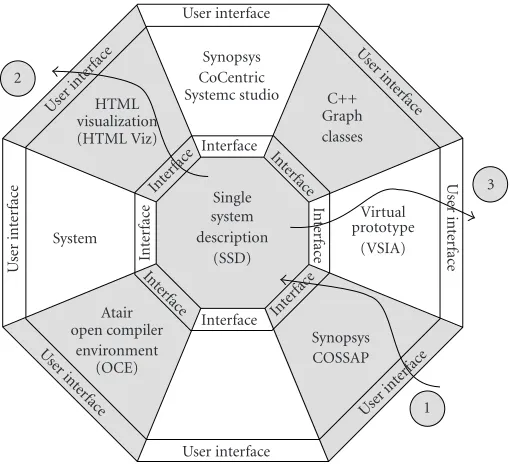
A framework reflecting these obligations is shown in Figure 1. It depicts the DDB surrounded by the required tools each with dedicated interfaces to incorporate the var-ious EDA tools and stays open for incorporating other tools as the empty tool box in the figure indicates. The various de-sign teams provide inputs, such as desired system behaviour and structure, constraints, and tool options. Also, the design-ers receive outputs, like status of the system description, re-sults of simulations, estimates of hardware costs, timing, and so forth. Typically, the outputs of the database are handed to the tools which present them in form of their GUIs to the de-signer. Some of the tools supported by the SSD are commer-cially available, favoured by the various design teams, while others are specially written to perform missing tasks, usually performed manually by designers in the past. As long as some design steps are not covered by available tools, for example HW/SW partitioning, a database modification tool is avail-able, simply allowing the designer to enter manually derived values. The database is thus enriched and the system descrip-tion is refined on its way to implementadescrip-tion. Note that the database system does not require a specific order of which various tools need to be performed. For example, some de-signers prefer to perform floating-point to fixed-point con-version after the HW/SW partitioning. As long as the suc-ceeding tool is provided with sufficient information, it can be started. Such open environment has not only the advan-tage that new commercial tools can be incorporated but it also provides a realistic platform to investigate the perfor-mance of new research tools. A possible design flow exam-ple is indicated inFigure 1. At first a COSSAP project is read into the SSD. In the second step the content of the database can be investigated over the HTML Visualization. As the last step, a virtual prototype is automatically generated out of the database content.
3.2. Inclusion of domain-specific modeling languages
User interface
User
inter
face Userint
erfa ce
U
ser
int
er
fa
ce
Synopsys CoCentric Systemc studio HTML
visualization (HTML Viz)
C++ Graph classes
Virtual prototype
(VSIA) System
Single system description
(SSD)
Atair open compiler
environment (OCE)
Synopsys COSSAP 2
3
1
U
ser
int
er
fa
ce
User inter
face U
ser int
er fa
ce
User interface Interface
Interface
In te
rface
In
te
rf
ac
e
Inte
rface
In
te
rf
ac
e
In te
rface
Inte
rface
Figure1: Interaction of the single system description with different design tools via interfaces providing a consistent design flow.
SDI
EDA tool Parser IF Scanner DDB
Figure2: Concept of the system description interface.
especially developed to represent the content of the database in a textual description, containing all relevant information, such as module instances, signal interconnections, and port declarations.
The SSD as the central repository of the consistent de-sign environment has been dede-signed to generally fit system descriptions and also design properties. The system descrip-tion part supports concepts as modules or entities, their hier-archy, and interconnections. This concept allows to store de-sign languages with concepts of parallel processing and pro-cedures. On the other hand, synchronous reactive languages like ESTEREL cannot directly be mapped to the DDB. The core of the underlying DDB structure is shown inFigure 3.
In addition to such concurrent concepts, sequential parts of system descriptions, such as processes and operation se-quences are also supported. The nomenclature of all concepts in the database structure implementing the single system de-scription was strongly inspired by SystemC. All entities that make up the system are instances of modules. These instances form one or more layers of hierarchy. Each of the instances can contain one or more processes. All processes in the sys-tem run concurrently. Processes are internally formed by ba-sic blocks. Within such baba-sic blocks sequences of operations are identified. Communication between instances, processes, and operations is achieved through data. Data connecting
several instances has several aliases; one within the context of each of the connected instances. An alias has an alias type, such as input, output, in-out port, or internal signal. Data has a data type, such as a signal, variable, or constant. Op-eration also has an opOp-eration type, such as addition (+), multiply-accumulation (MAC), or left bitwise shift ().
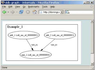
Figure 4shows a graphical representation of a small de-sign written in SystemC. Example 1 which is an instance of Example has inputs (in1, in2, in3, in4) and an output (out1). It contains three blocks: two adders (add 1, add 2) and one multiplication (mul 1), and their corresponding processes. The add blocks are connected with the multiplier internally with the signals int1 and int2. Here, the alias concept is use-ful to identify these signals with the internal output signals of the add blocks and the input signals of the multiplier. A cut-out of the XML-based IF of this example is presented in Figure 5.
A scanner tool processes this IF and enriches the DDB accordingly. In this simple case the module table holds the names for the used modules Example, add, and mul. Inside of the instances table, Example 1, add 1, add 2, and mul 1 can be found and the alias table stores the ports in 1, in 2, in 3, in 4, out 1, and the internal signals int1 and int2. The two-stage structure facilitates the development of new in-terfaces in such a way that the developer of the parser can neglect everything related to database management, that is, adding or deleting modules, removing redundant informa-tion, updating of attributes and so forth. This task is fulfilled by the scanner tool, which depends only on the IF and the current contents of the DDB.
Design properties System description
Process
property Process Instance
Module
Block property
Basic block
Basic block con
Operation Data Alias
Operation
type Datatype
of type
has
has reads
writes
is of is of
has has
has has
has has
Hierarchy
Figure3: The structure of the design database (DDB).
Example 1 (Example)
add 1 (add) in1
in2
in3
in4
Addition
add 2 (add)
Addition
int1
int2
mul 1 (mul)
Multiplication out1
Figure4: Design example.
at system level. To provide a complete representation of the COSSAP model within the DDB, the information on the architectural structure as well as on the functionality and behaviour of each component is extracted from the COS-SAP project. A COSCOS-SAP project stores its model architecture in a nonhierarchical way in a file pair named after the top module, suffixed “.v arc” and “.v ent.” The description lan-guage used in these files is VHDL compliant. A parser for VHDL has been implemented to create the IF representation of the model architecture (see left-hand part ofFigure 10 fur-ther ahead). This parser is based on two open source tools: Flex (www.gnu.org/software/flex/flex.html), a lexical ana-lyzer, and Bison(www.gnu.org/software/bison/bison.html), a parser generator. The scanner, a set of PERL scripts,
Figure5: XML-based intermediate format.
Figure6: HTML visualisation of the database content. Hierarchical view of the modules.
Figure7: HTML visualisation of the database content. Data flow graph of modules.
the algorithmic design team and were thus quickly adopted throughout the algorithmic design team. While other SDIs for the SSD exist (e.g., for reading SystemC v1.0 designs), we will focus on the COSSAP SDI in this paper.
3.3. HTML visualisation
As mentioned before, some design steps are not supported by automatic tools yet. To facilitate manual interaction with designer, GUIs for viewing information and changing en-tries are provided. To support the designers working on the development of the system, whose description resides in the database, with a visual representation of the system, an HTML visualisation over a web browser has been developed. This software program, implemented as a PERL CGI script, provides an easily extendable view of the database contents. Since it is a CGI script, a dynamic view of the system descrip-tion, immediately reflecting any changes and updates, is pro-vided. Different views of the database content can be repre-sented over a browser. For example, the hierarchy of instances in the system is represented graphically (Figure 6), where it can be seen that the modules add 1, add 2, and mul 1 are in-stantiated inside the module Example 1.Figure 7depicts the data flow graph of the modules in Example 1.
4. VIRTUAL PROTOTYPING
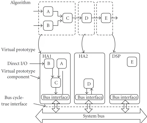
The HW/SW partitioning process transforms a system-level specification into a heterogeneous architecture composed of hardware and software modules. A software simulation of this simulatable model is called virtual prototype (VP) [13,14,15,16]. Generally, the VP reflects a platform-based design (PBD), typically a DSP surrounded by multiple HW accelerators (HA). Those HW accelerators are called VP components if they are used inside a VP simulation. Sev-eral properties of abstraction layers are proposed for a VP, as they can be time related (e.g., untimed, timed functional, bus-cycle accurate, cycle true), data related (e.g., floating-point and fixed-floating-point representations), and communication related (e.g., synchronous data flow (SDF), transaction-level modeling (TLM) [36], open core protocol international part-nership OCP [37]).
A crucial point in the partitioning for a SoC-design is a carefully designed interface, connecting hardware and soft-ware parts. Whereas hardsoft-ware development, and especially its testing, can be done rather independently from the soft-ware development, development and testing of the softsoft-ware has to wait until the hardware has been designed. In the case of an application-specific integrated circuit (ASIC), verifi-cation cannot start until the first engineering samples have been manufactured (Figure 8).
The VP technique on the other hand enables earlier de-velopment and testing of the software. In this technique, SW reflects the behaviour of the HW and implements the HW interface to the SW, as it will be realised later in HW. Such a VP can be implemented faster than the HW itself, because all the HW implementation details specific to the chosen technology can be neglected and high-level description lan-guages can be used instead of hardware description lanlan-guages (HDLs).
Other advantages of a VP are its capability to serve as a reference (golden) model for the HW accelerators, whose functionality it mirrors at the bus interface as well as to sup-port refinement steps: a first version of the VP can be gen-erated without considering any architecture or timing (un-timed). Then, in a next step, the specific HW target platform can be included with a DSP-core element, a bus, and various HW accelerators, which communicate bus-cycle accurate. As a last step, the internal behaviour of the HW accelerators has to be transformed to a cycle-true model. This step is usu-ally called high-level synthesis and is investigated by many research projects like for example in [38] and also adopted in commercially available tools (behavioural compiler from SYNOPSYS). A survey of high-level design transformation techniques is given in [39]. In that sense, VP also supports a refinement-step-based design, which allows a much more consistent forgoing than switching between description lan-guages.
4.1. On automatic VP generation
Traditional design cycle
Algorithmic
Hardware
Software
System design cycle with VP
Algorithmic
VP
Hardware
Software
Automatic VP generation
Algorithmic
VP (automatic)
Hardware
Software
Time savings = profit boost
Time savings = profit boost
Figure8: Decrease of design time by virtual prototyping and automatic generation of virtual prototypes.
A
B
C D E
B A
C D
E
HA1 HA2 DSP
Bus interface Bus interface Bus interface
System bus Algorithm
Virtual prototype
Direct I/O
Virtual prototype component
Bus cycle-true interface
Figure9: Reuse of algorithmic description for virtual prototype generation.
Figure 8. Specific results utilizing this method are reported inSection 6.
A DSP structure enriched by hardware accelerators com-municating via a common bus was selected for the design requiring the VP to reflect the DSP as well as to support its hardware accelerators communication (see alsoFigure 12 further ahead). Note that at the algorithmic level, the de-sign information is free of communication details. Thus, in order to achieve communication of the VP components via the chosen PBD, an object-oriented environment in C++ has been created, containing classes for functional blocks, ports, FIFOs, and scheduling. While this implementation implies
a certain HW platform, much emphasis was put on the fact that this platform is very general, a DSP with a common bus structure for its HW accelerator units. The automatism was implemented for COSSAP designs based on GenericC de-scriptions only. However, the methodology was left open for supporting other descriptions, like SystemC.
HW/SW partitioning information
table
COSSAP
∗.v arc ∗.v ent
∗.gc
COSSAP guidelines
System description interface (SDI)
for COSSAP
Design
data-base (DDB)
VPG
VP components
Bus interface
C A
B Scheduler
Figure10: Design process for VP generation.
In
In
In
FIFO
FIFO
FIFO · · ·
bool executeCheck() · · ·
Bool BLOCK run() · · ·
CDLPort<Int>InFixed; CDLPort<float>InData; CDLPort<int>InSoft; CDLPort<int>OutData; CDLPort<int>OutFixed; · · ·
CDLBlock∗∗succlist; // Member list for // BLOCK run() · · ·
Out
Out
List of next input ports
List of next input ports
Class Channel Decoding: public CDLBlock
Figure11: A virtual prototype block class.
shortened considerably by reusing the algorithmic descrip-tion for the DSP accelerators. Such devices are simply mod-eled by a register interface that can be accessed by the DSP via a common bus. It is thus only necessary to model the processing unit (StarCore-DSP) by an instruction-set simu-lator (ISS) running the SW part of the design. All other mod-ules later being realized as hardware accelerators are simply copied from the COSSAP description also supporting veri-fication of the design. Moreover, a VP with such properties can serve as a base for prototyping and still be used for fur-ther refinements steps towards a whole cycle-true design.
The implementation of such a VP representation needs a simulation environment that allows for simulation of par-allel processes. Hardware description languages like SystemC and VHDL can be used for that task, because they provide statements for concurrent processing. For the presented VP another simulation interface has been chosen, that has been proposed by the Virtual Socket Interface Association (VSIA) [17]. This VSIA-compliant simulation uses a static schedul-ing, achieving faster simulation compared to the event-based simulation of SystemC and VHDL. Even compared to a plain C++ implementation, the VSIA implementation introduces negligible overhead.
Thus as already mentioned in Section 2, some ap-proaches for an automatic partitioning into HW/SW parti-tioning exist, partiparti-tioning in real-world examples is based on much more complicated scenarios even often not based on technical issues. Sometimes implementation in software is preferred in order to stay as long as possible flexible to react to changes in the standard for the implemented algorithm. For this reason the HW/SW partitioning information can be performed manually based on the experience of the various design engineers. This information is manually written into a so-calledHW/SW partitioning table(HSP), an extension to the DDB. It is possible to flag each single instance or each instance of a certain module type of the system description ashardwareorsoftware(Figure 10). Automatic partitioning embedded in the presented design flow is discussed in [40].
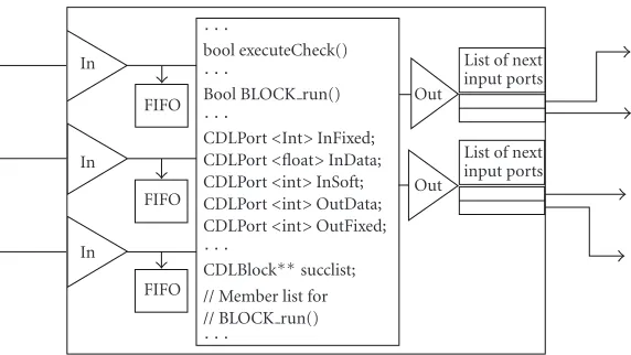
For each module supposed to be implemented in hard-ware, a C++ file pair, consisting of header and class file, is created automatically. These module classes are derived from the CDLBlock class, which is the centre of the VP component infrastructure.Figure 11depicts the outline of such a mod-ule.
is the “BLOCK run().” In this procedure the extracted and styled functional part of the GenericC code from a COSSAP project is inserted automatically. Also a C++ file pair for the top module, containing the structure of the VP component, is created automatically. Within the constructor of this class, all instances characterised as HW are instantiated and inter-connected.
Furthermore, an additional function is provided to ver-ify that sufficient data for at least one execution of a block is available at the input ports supporting the scheduling capa-bilities of the VP design. The top module class has a member function acting as a scheduler. Assuming a directed graph structure of the architecture, a scheduler was implemented obeying a recursive depth-first search algorithm [41]. On this account, each block manages a list of its successors which has been set up when the interconnections of all instances were established. The scheduler is responsible for calling each block as often as possible, that is, as long as sufficient data is supplied at the input ports.
Such automatic VP generation requires to restrict the programming freedom of the algorithmic designers. A design style sheet providing guidelines withdo’s and don’tswas pro-vided to the algorithmic designers. These guidelines include naming conventions for ports, as well as for the correspond-ing data rates, and internal states of the modules in COSSAP, in order to allow simple and unique automatic recognition. For example, over input ports of each block in the COS-SAP design data, values or parameters can be applied, but in the architectural implementation they are handled differ-ently. In order to automate the VP generation it is necessary to give a dedicated prefix to each port name (Input para or Input data). According to that naming convention also the names for the port rates require a prefix (Rate Input para or Rate Input data). The algorithmic designers did not find such guidelines very restricting and quickly adopted their al-gorithmic design towards it. This step allowed to convert a fixed-point design from algorithmic design level to VP auto-matically.
Previous implementations of VPs have for the most part focused on their use, in the hardware/software cosimulation of the embedded system [15,42]. While these early efforts are targeted towards increasing the efficiency and quality of the design process through novel modifications of the cosimula-tion process, a transicosimula-tion method (even a manual one) from an algorithmic description to the VP was not shown. A first automatic approach is presented in [14] achieving a speedup in the order of five to eight times compared to a manual VP creation, but it does not support PBDs. In particular, it does not consider the architectural needs of complex SoC, consist-ing of several hardware accelerators, and a bus system.
5. CONSISTENT TESTING BY AUTOMATIC TOOLS
According to [15,22] about 70% of development time is ver-ification and testing in 3G wireless designs. Time-consuming parts of testing are the individual test pattern generations performed manually for each design level. It is thus very
DMA StarCoreDSP
HA1 HA2
RAM
Direct I/O
System bus
· · ·
Figure12: Target hardware platform based on a StarCore DSP.
beneficial to convert these test patterns starting from the al-gorithmic level automatically down to the subsequent levels. At the VP level, a decision of HW/SW partitioning has been made. The test patterns for the individual blocks have to be provided in a certain order and size as well as in a format specified at the VP design. Thus, the challenge in testing is to provide means for automatically converting high-level test patterns into these specific formats.
5.1. Overview of hardware platform
While the testing process in general is rather independent of the HW platform, the actual format is not. Therefore, we first describe more details of the HW platform utilising a Star-Core DSP(www.starcore-dsp.com). The hardware platform targeted in this work is a SoC based on a StarCore DSP, as represented inFigure 12.
In addition to the StarCore DSP, the platform includes several hardware accelerators. Just like the DSP, the HA blocks are connected through the system bus to all the other components. Additionally direct I/O interface for HAs are provided, which can be used to connect to components out-side the embedded SoC, such as the antenna subsystem. The platform also includes a bank of random access memory (RAM) for use by all the system components. Direct mem-ory access (DMA) services are provided to the DSP, as well as to the HA by a dedicated DMA controller, which is also connected to the system bus.
After HW/SW partitioning is performed on the algorithmic-level description of the system, the algorithmic functions assigned to hardware are implemented as separate HAs, whereas functions assigned to software are realized in software running on the DSP.
5.2. Reuse of test patterns
Data in
Data out
Parameter in
Parameter out
Test generator
script
Formal interface specification
Direct I/O programC test Memory image
StarCore testcase
Figure13: Automatic environment for reuse of test patterns.
ascertained that both the VP model and eventually its hard-ware implementation are functionally equivalent to the orig-inal COSSAP model. For this purpose, the automatically generated verification environment presented here reuses all test patters in the COSSAP model and applies them to both the VP and the HW model. Both models exist as part of the same platform (seeFigure 12) and for this reason each VP component is tested with the same test bench in both envi-ronments.
The automatic environment for reuse of test patterns is shown inFigure 13. The test bench consists of a C program running on the StarCore DSP, a memory image resident in the system’s RAM, as well as direct I/O test patterns to be supplied to the VP component during testing. The verifica-tion environment includes the automatic generaverifica-tion of test benches immediately from COSSAP test patterns. The inputs into the test generator script (TGS) are a formal specification of the interface between the StarCore DSP and the VP com-ponent under test as well as the data and parameter dump files containing the COSSAP test patterns. The output of the test generator script is a test bench, which runs in both the VP simulation environment and on the actual hardware plat-form.
TGS creates a memory image containing the test patterns, suitably annotated with the timing information (as found in the COSSAP dump files) and the VP component interface information (as found in the formal interface specification). The C test program is generic and is therefore applicable to any memory image and thus any test bench, without modi-fication. In other words, all case-specific information is cap-tured in the memory image only. When the test patterns in COSSAP include direct I/O data, such data is simply copied into the test bench and applied directly to the VP compo-nent through its I/O ports, both in the VP simulation and on the actual HW platform. It is not stored in the memory image, because it is not communicated to the VP component through the system bus and is thus not handled by the C test program.
5.3. The VP as golden model for the HW
At the time the VP has been automatically created and its functionality at the bus interface has been tested using the verification environment explained in the section before, it can be further used as a golden model for the HW develop-ment.
The VP component organises the synchronous data flow between its inner functional components using a FIFO class. In order to provide a verification facility while running a VP simulation, the implementation of the FIFO blocks in-cludes a bi-directional insertion/extraction feature. In other words, in addition to simply being passed from one func-tional block to another, data probes can be handed to output (dump mode) files as well as read from input files (pump mode) independently. This file input/output functionality exists in every FIFO in the VP model and thus offers max-imum flexibility in inspecting and/or inserting test patterns at any point within the VP structure, depicted inFigure 14. Provided that the HW developer organises the internal HW accelerator design in the same functional fragmentation (e.g., a corresponding VHDL entity for each C++ class in the VP component), the test patterns generated by the VP blocks can be adopted to verify the proper functionality of the VHDL entities.
Note that the fragmentation into several blocks in the VP component is very coarse as it mirrors the highest abstrac-tion level, the algorithmic descripabstrac-tion in COSSAP. Thus the impact on the creativity of the HW developer with respect to design and optimisation issues at the RT-level is negligible. Experience from HW development (by industrial collabora-tion) revealed that the demand for test patterns at predefined points is much higher than the demand for less structural re-quirements.
As mentioned before the internal representation of the VP component is generally untimed to offer highest simu-lation speed, just in opposition to the cycle-true HW im-plementation. Therefore, the data probes from the VP can-not contain timing information below the bus-cycle accurate level. Since the sequence of the values, sent from one inter-nal block to the next, remains unaffected, the verification of the corresponding VHDL entities is enabled. A file format has been defined which captures the necessary information to identify the source block, the port name, the bus cycle, and the numbering of the generated value. A convenient way to analyse the corresponding test pattern files is via the Open Source tool TkDiff (http://sourceforge.net/projects/tkdiff/), offering graphical support for the comparison of text files.
6. EXAMPLES OF UMTS DESIGNS
HW/FW interface
VP peripheral (C++)
BlockX.cpp BlockY.cpp BlockZ.cpp
Test in Test out
HW/FW
interface BlockX.cpp BlockY.cpp BlockZ.cpp
HW peripheral (VHDL)
Bu
s
Bu
s
TkDiffGUI
Test in Test out
Figure14: VP as a golden model for HW implementation.
HW/FW interface
Parameter
Data
Configuration
Deinterleaving
CRC check
Scheduler
DTX removing
Segmentation into code blocks
Rate matching
Channel decoding
Bu
s
Class DUD: public CDLVp
Figure15: VP block diagram of the peripheral for decoding of user data (DUD).
more thoroughly in the following. Each of the four parts re-alizes the complete or partial functionality of (a) delay pro-file estimation (DPE), (b) frame and slot synchronisation (SYNC), (c) rake receiver (RAKE), and (d) decoding of user data (DUD). As a detailed example, Figure 15depicts the DUD peripheral to expose the VP infrastructure of the au-tomatically generated HW peripheral.
This DUD consists of six blocks, representing the digi-tal signal processing for the decoding of user data accord-ing to 3GPP TS25.212, and additional three blocks ( config-uration, HW/FW-interface, and scheduler) generated by the VP in order to support scheduling. Theconfigurationblock collects the initial parameters of the six signal processing blocks, which cannot be passed by the HW/FW interface
during run-time and delivers them to each block to set up the specific behaviour, for instance switching the data pro-cessing from a slot to a frame basis. Note that the COS-SAP developer has the possibility to change the parame-ters of a block before each block invocation. In the VP as well as in the real HW implementation this is different;
it is only possible to update the parameters of the blocks between two peripheral invocations. The HW/FW interface
communicates via the on-chip bus with the StarCore DSP, configures the DUD peripheral, fills the FIFOs of the dein-terleaving block with data and triggers the scheduler func-tion.
Table1: Algorithmic complexity and time expense of the manually generated VP peripherals (PH=person hour, LOC=lines of code).
HW peripheral LOC PH PH/LOC
DPE 1653 25 0.015
SYNC 2422 39 0.016
DUD 2398 43 0.018
Table2: Infrastructural complexity and time expense of the man-ually generated VP peripherals (PH=person hour, NIB=number of instantiated blocks).
HW peripheral NIB PH PH/NIB
DPE 5 8 1.60
SYNC 7 17 2.43
DUD 6 12 2.00
In a second step, the creation of the C++ files for the top module, which instantiates, interconnects, and config-ures the blocks, has been accomplished. The time spent is assumed to be proportional to the number of instantiated blocks (NIB), further on referred to as infrastructural com-plexity. The results are listed in Table 2 showing an avg. PH/NIB=2.0.
As the HW/FW interface has to be described manually with respect to the underlying architecture, its development time is not taken into account for the evaluation of time re-duction. Assuming that the averaged values of the PH/LOC and PH/NIB ratios obtained from UMTS receiver are reliable metrics for the remaining peripherals of the whole UMTS BPU, it is possible to estimate the design effort for the man-ual generation of all VP peripherals. An amount of 774 PH for 121 NIBs and 31 266 LOCs was estimated. Employing the presented automatic approach, each of the VP peripherals is generated within seconds.
Note that in an industrial development such mapping from the fixed-point algorithmic model to the VP model is not performed just once. Many revision levels are required until the functionality of all modules is satisfactory. Now, in the middle of the design process, our development routine revealed revision levels for the peripherals of already more than fifty; and at each revision version, in which especially the infrastructure (e.g., number of ports, connections) has been changed to a certain degree, this approach exposes its superior performance, applying the automatic mapping pro-cedure. The time savings accumulate to many thousand per-son hours over an entire design. Its application in an indus-try project, where an ISS of a StarCore together with the debugging facilities of the CodeWarrior environment from Metrowerks has been used, proved that the modification of an existing COSSAP project necessary to be compliant to the GenericC guidelines causes negligible effort, while the speedup of development time is substantially. Note, however, that this simple arithmetic does not show the only benefit of the proposed method. A manual process would have con-sumed not only thousands of additional hours but also many more hours required to find the manually generated bugs, whereas an exhaustively tested tool is almost error free.
7. CONCLUSIONS
The automated environment for VP generation presented here has been successfully applied in an industrial design flow, showing significant speedup in creation of VPs, with savings in the order of hundreds of person hours per revision. Simultaneously, this approach also eliminates human-related errors, thus improving quality. Additionally, work presented here shows better performance benefits, increased flexibil-ity, and wider applicability compared to previously presented automated techniques. Future work on the presented envi-ronment includes generation of VPs in standards other than VSIA, such as SystemC, CoMET from Vast System Tech-nology (www.vastsystems.com), or SEAMLESS from Men-tor Graphics (www.mentor.com). Also processing of algo-rithmic descriptions developed in environments other than COSSAP are of interest. Furthermore a direct binding of the presented VP environment with more of the numerous com-mercial algorithmic- and architecture-level tools is expected to increase automation and thus significantly gain design ef-ficiency.
ACKNOWLEDGMENTS
The authors would like to acknowledge the ongoing coop-eration with Infineon Technologies and in particular thank Thomas Herndl, Ahmad Sarashgi, Wolfgang Haas, Sasha Simeunovic, and Johann Glaser for their collaboration. This work has been funded by the Christian Doppler Laboratory for Design Methodology of Signal Processing Algorithms.
REFERENCES
[1] G. Moore, “Cramming more components onto integrated cir-cuits,”Electronics Magazine, vol. 38, no. 8, pp. 114–117, 1965. [2] P. Fisher and D. Cottrell, “Emerging standards in the elec-tronic design automation (EDA) industry,” inElectronic Sys-tems Design Seminar, UC Berkeley, Calif, USA, October 1999. [3] R. Subramanian, “Shannon vs Moore: the digital signal pro-cessing in the broadband age,” inProc. IEEE Communication Workshop, Aptos, Calif, USA, May 1999.
[4] R. Subramanian, “Shannon vs Moore: driving the evolution of signal processing platforms in wireless communications,” in Proc. IEEE Workshop on Signal Processing Systems (SIPS ’02), San Diego, Calif, USA, October 2002.
[5] P. Belanovi´c, M. Holzer, D. Miˇcuˇs´ık, and M. Rupp, “Design methodology of signal processing algorithms in wireless sys-tems,” inProc. International Conference on Computer, Com-munication and Control Technologies (CCCT ’03), pp. 288– 291, Orlando, Fla, USA, July 2003.
[6] M. Holzer, P. Belanovi´c, and M. Rupp, “A consistent design methodology to meet SDR challenges,” inWireless World Re-search Forum (WWRF9 ’03), Zurich, Switzerland, July 2003. [7] R. Baines and D. Pulley, “A total cost approach to evaluating
different reconfigurable architectures for baseband process-ing in wireless receivers,”IEEE Commun. Mag., vol. 41, no. 1, pp. 105–113, 2003.
[8] R. Leupers and P. Marwedel, “Retargetable code generation based on structural processor descriptions,”Design Automa-tion for Embedded Systems, vol. 3, no. 1, pp. 1–36, 1998. [9] J. Brakensiek, B. Oelkrug, M. Bucker, et al., “Software radio
Mobile Radio Communications (PIMRC ’02), vol. 1, pp. 110– 114, Lisboa, Portugal, September 2002.
[10] P. M. Heysters, H. Bouma, J. Smit, G. J. M. Smit, and P. J. M. Havinga, “A reconfigurable function array architecture for 3G and 4G wireless terminals,” inProc. World Wireless Congress (WWC ’02), pp. 399–405, San Francisco, Calif, USA, May 2002.
[11] J. R. Hauser and J. Wawrzynek, “Garp: a MIPS processor with a reconfigurable coprocessor,” inProc. 5th Annual IEEE Sym-posium on FPGAs for Custom Computing Machines (FCCM ’97), pp. 12–21, Napa Valley, Calif, USA, April 1997.
[12] M. B. Taylor, J. Kim, J. Miller, et al., “The Raw microproces-sor: a computational fabric for software circuits and general-purpose programs,”IEEE Micro, vol. 22, no. 2, pp. 25–35, 2002.
[13] C. A. Valderrama, A. Changuel, and A. A. Jerraya, “Virtual prototyping for modular and flexible hardware-software sys-tems,”Design Automation for Embedded Systems, vol. 2, no. 3-4, pp. 267–282, 1997.
[14] A. Hemani, A. K. Deb, J. Oberg, A. Postula, D. Lindqvist, and B. Fjellborg, “System level virtual prototyping of DSP SOCs using grammar based approach,”Design Automation for Em-bedded Systems, vol. 5, no. 3-4, pp. 295–311, 2000.
[15] A. Hoffmann, T. Kogel, and H. Meyr, “A framework for fast hardware-software co-simulation,” inProc. Design, Automa-tion and Test in Europe (DATE ’01), pp. 760–765, Munich, Ger-many, March 2001.
[16] N. Voros, L. S´anchez, A. Alonso, A. Birbas, M. Birbas, and A. Jerraya, “Hardware/software co-design of complex embedded systems: an approach using efficient process models, multi-ple formalism specification and validation via co-simulation,” Design Automation for Embedded Systems, vol. 8, no. 1, pp. 5– 49, 2003.
[17] U. Bortfeld and C. Mielenz, “C++ system simulation inter-faces,”Whitepaper, July 2000.
[18] R. Ernst, J. Henkel, and T. Benner, “Hardware-software cosyn-thesis for microcontrollers,”IEEE Des. Test. Comput., vol. 10, no. 4, pp. 64–75, 1993.
[19] T. Wiangtong, P. Y. K. Cheung, and W. Luk, “Comparing three heuristic search methods for functional partitioning in hardware-software codesign,”Design Automation for Embed-ded Systems, vol. 6, no. 4, pp. 425–449, 2002.
[20] T. Blickle, J. Teich, and L. Thiele, “System-level synthesis us-ing evolutionary algorithms,”Design Automation for Embed-ded Systems, vol. 3, no. 1, pp. 23–58, 1998.
[21] CoWare, “SoC platform-based design using Conver-genSC/SystemC,” July 2002,http://www.coware.com. [22] B. Bailey, “The Waking of the Sleeping Giant-Verification,”
April 2002,http://www.mentor.com/consulting/techpapers/. [23] U. Gl¨asser, R. Gotzhein, and A. Prinz, “The formal semantics
of SDL-2000: Status and perspectives,”Computer Networks, vol. 42, no. 3, pp. 343–358, 2003.
[24] T. Gr¨otker, S. Liao, G. Martin, and S. Swan,System Design with SystemC, Kluwer Academic, Boston, Mass, USA, 2002. [25] M. Coors, H. Keding, O. L¨uthje, and H. Meyr, “Design and
DSP implementation of fixed-point systems,” EURASIP J. Appl. Signal Process., vol. 2002, no. 9, pp. 908–925, 2002. [26] M. Rupp, A. Burg, and E. Beck, “Rapid prototyping for
wire-less designs: the five-ones approach,”Signal Processing, vol. 83, no. 7, pp. 1427–1444, 2003.
[27] F. Balarin, E. Sentovich, M. Chiodo, et al.,Hardware-Software Co-Design of Embedded Systems: The POLIS Approach, Kluwer Academic, Boston, Mass, USA, 1997.
[28] G. Berry, S. Moisan, and J. Rigault, “ESTEREL: Towards a synchronous and semantically sound high level language for real-time applications,” inProc. IEEE Real-Time Systems Sym-posium (RTSS ’83), pp. 30–37, IEEE Computer Society Press, Arlington, Va, USA, December 1983.
[29] N. Halbwachs, P. Caspi, P. Raymond, and D. Pilaud, “The syn-chronous data flow programming language LUSTRE,”Proc. IEEE, vol. 79, no. 9, pp. 1305–1320, 1991, Special Issue “An-other Look at Real-Time Programming”.
[30] J. Buck, S. Ha, E. A. Lee, and D. G. Messerschmitt, “Ptolemy: a framework for simulating and prototyping heterogeneous systems,”International Journal in Computer Simulation, vol. 4, no. 2, pp. 155–182, 1994, Special Issue on Simulation Software Development.
[31] J. Sztipanovits, “Advances in model-integrated computing,” in Proc. 18th IEEE Instrumentation and Measurement Technology Conference (IMTC ’01), vol. 3, pp. 1660–1664, Budapest, Hun-gary, May 2001.
[32] G. Karsai, J. Sztipanovits, A. Ledeczi, and T. Bapty, “Model-integrated development of embedded software,”Proc. IEEE, vol. 91, no. 1, pp. 145–164, 2003.
[33] J. Gray and G. Karsai, “An examination of DSLs for concisely representing model traversals and transformations,” inProc. 36th Annual Hawaii International Conference on System Sci-ences (HICSS ’03), vol. 9, Big Island, Hawaii, USA, January 2003.
[34] G. Karsai, “Design tool integration: an exercise in seman-tic interoperability,” inProc. 7th IEEE International Confer-ence and Workshop on the Engineering of Computer Based Systems (ECBS ’00), pp. 272–278, Edinburgh, UK, April 2000.
[35] J. Groff and P. Weinberg, SQL: The Complete Reference, McGraw-Hill, Osborne, Emeryville, Calif, USA, 2nd edition, 2002.
[36] L. Cai and D. Gajski, “Transaction level modeling in system level design,” Tech. Rep., Center for Embedded Computer Sys-tems, Irvine, Calif, USA, 2003.
[37] A. Haverinnen, M. Leclercq, N. Weyrich, and D. Wingard, “White Paper: SystemC based SoC Communication Modeling for the OCP Protocol,” OCP International Partnership, Port-land, Ore, USA, October 2002.
[38] S. Gupta, N. Dutt, R. Gupta, and A. Nicolau, “SPARK: A high-level synthesis framework for applying parallelizing com-piler transformations,” in Proc. 16th International Confer-ence on VLSI Design, pp. 461–466, New Delhi, India, January 2003.
[39] W. Wu and A. Jantsch, “A survey of design transfor-mation techniques,” Tech. Rep., Departement of Electron-ics, Royal Institute of Technology, Kista, Sweden, 1999. http://www.ida.liu.se/∼eslab/SAVE/.
[40] B. Knerr, M. Holzer, and M. Rupp, “HW/SW partitioning us-ing high level metrics,” inProc. International Conference on Computing, Communications and Control Technologies (CCCT ’04), pp. 33–38, Austin, Tex, USA, August 2004.
[41] R. Sedgewick, Algorithms, Addison-Wesley, Boston, Mass, USA, 1988.
P. Belanovi´c received his B.E. and M.S. degrees from the University of Auckland, New Zealand, and Northeastern University, Boston, in 2000 and 2002, respectively. His research focused on the acceleration of im-age processing algorithms with reconfig-urable platforms, both in remote sensing and biomedical domains, as well as custom-format floating-point arithmetic. Currently he is a Ph.D. candidate at the Vienna
Uni-versity of Technology, Austria, focusing on the design method-ologies for embedded systems in wireless communications, virtual prototyping, and automated floating-point to fixed-point conver-sion.
B. Knerr studied communications en-gineering at the University of Saarland and the Technical University of Hamburg-Harburg, respectively. He finished the Diploma thesis about OFDM communica-tions systems and graduated with honours in 2002. He worked for one year as a soft-ware engineer for the UZR GmbH & Co KG, Hamburg, on image processing and 3D computer vision. In June 2003 he joined the
Christian Doppler Laboratory for Design Methodology of Signal Processing Algorithms at the Vienna Technical University as a Ph.D. candidate. His research interests are in HW/SW partitioning, mul-ticore task scheduling, static code analysis, and platform-based de-sign.
M. Holzerreceived his Dipl.-Ing. degree in electrical engineering from the Vienna Uni-versity of Technology, Austria, in 1999. Dur-ing his Diploma studies, he worked on the hardware implementation of the LonTalk protocol for Motorola. From 1999 to 2001 he worked at Frequentis in the area of auto-mated testing of TETRA systems and after-wards until 2002 at Infineon Technologies on ASIC design for UMTS mobiles. Since
2002 he has a research position at the Christian Doppler Labora-tory for Design Methodology of Signal Processing Algorithms at the Technical University of Vienna.
G. Sauzon received his Engineer degree from ENSERG, Grenoble, France. He joined Infineon Technologies in 1999, focusing on the architecture definition of a UMTS re-ceiver. His work also included analysis of design flows and development of virtual prototypes for architecture verification. His current interests are focused on verification of baseband processors.
M. Ruppreceived his Dipl.-Ing. degree in 1988 from the University of Saarbr¨ucken, Germany, and his Dr.-Ing. degree in 1993 from the Technische Universit¨at Darmstadt, Germany, where he worked with Eber-hardt H¨ansler on designing new algorithms for acoustical and electrical echo compen-sation. From November 1993 until July 1995 he had a postdoctoral position at the