Study of Scan Blindness of Microstrip Array by Using
Dumbbell-Shaped Split-Ring DGS
Chandan K. Ghosh1, *, Susmita Biswas2, and Durbadal Mandal2
Abstract—A compact dumbbell-shaped split-ring DGS is introduced between array elements of a sixteen-element microstrip array in order to reduce the mutual coupling between antenna elements and eliminate the scan blindness. The proposed DGS is inserted between the adjacent rectangle-shaped slotted microstrip antenna elements separated by 0.35λ, as a technique to suppress the radiation in the horizontal direction. Simulated results show that a reduction in mutual coupling of 36 dB is obtained between elements at the operation frequency of 2.45 GHz (WLAN band). The scan properties of microstrip array with and without DGS have been studied, and the result indicates that the scan blindness of the array has been well eliminated because of the effect of the DGS. We have developed experimental models that have proved the concept of scan blindness elimination. Finally, the influence of other antenna parameters at the presence of DGS in the array system has been studied. Prototype antennas of sixteen-element array with and without resonator have been fabricated, measured, and the idea has been verified. A good agreement is observed between measured and simulated results.
1. INTRODUCTION
To obtain compact size and wide bandwidth, a substrate with higher permittivity and a thicker profile has been extensively used in the microstrip antenna design. However, this substrate results in the increased surface wave excitation. In a microstrip array, the severe surface waves increase the mutual coupling between array elements, which cause impedance and pattern anomalies associated with the blind angle [1–4]. To suppress surface waves in a microstrip substrate, an important approach is to use electromagnetic bandgap (EBG) structures. The mushroom-like EBG structures with insertion of conductive fences or vias have been applied to reduce the element mutual coupling and eliminate scan blindness of the microstrip phased array. However, few researches focus on suppressing element mutual coupling and eliminating scan blindness in a microstrip phased array based on DGS techniques. The scan blindness occurs before the onset of the grating lobe, requiring the re-calculation of element spacing to maintain the scan blindness out of the required scanned area. For an array antenna, the onset of the grating lobe is determined from the following relationship—
D λ0
= 1
1 +|sinθm| (1)
where, D= element separation, λ0 = free-space wavelength, andθm = maximum angular scan.
For a printed array of patches on a grounded dielectric, the problem is complicated by the presence of surface waves supported by the dielectric. The thicker is the dielectric material, the larger is the number of surface waves propagating within the dielectric material. In this case, it is assumed that the thickness of the material ‘d’ is chosen such that
d < λ0
4√εr−1 (2)
Received 14 August 2014, Accepted 22 October 2014, Scheduled 28 October 2014
* Corresponding author: Chandan Kumar Ghosh (mcet [email protected]).
where εr = dielectric constant of the material, so that only the lowest-order surface wave, TM0, can propagate. The presence of the TM0 surface wave causes scan blindness in theE-plane. The angle at which this scan blindness occurs is closer to bore sight than the onset of the grating lobe.
In this work, a dumbbell-shaped split-ring DGS has been incorporated in between array elements for the suppression of scan blindness of antenna array. The DGS has been optimized to suppress scan blindness at 2.45 GHz.
In [5] by Nikolic et al., a general technique has been proposed to compensate surface currents in the ground plane and suppress radiation in horizontal directions. In [6] by Zhang et al., scan blindness has been studied by using photonic band-gap (PBG) substrate, and scan blindness has been significantly eliminated.
In [7] by Iluz et al., uniplanar compact electromagnetic bandgap (UC-EBG) substrate has been used to reduce surface wave excitation in printed antenna geometries. The results show a reduction in mutual coupling between elements and provide a possible solution to the “blind spots” problem in phased array applications with printed elements. In [8, 9], EBG structures have been used to tackle the surface-waves of rectangular microstrip patch arrays.
Mutual coupling has a direct impact on the performance of multi-element antenna systems. The interaction between elements degradesS-parameters, and as a result, the scan blindness of the radiation pattern for the adjacent E-plane coupled elements in the array increases.
The coupling can result in severe degradation to the antenna’s radiation characteristics. While surface waves are weakly excited in very thin grounded dielectric substrates, space-waves dominate and show strong coupling when antennas are in close proximity [10]. In [11], a compact DGS structure has been used to eliminate blindness of a phased array antenna. The works stated above either suffer from high back radiation or compactness.
In our investigation, a simple and efficient technique is proposed to suppress the effect of scan blindness between two closely spaced antenna elements. We have used a simple dumbbell-shaped split-ring DGS between two E-shaped microstrip antennas, and mutual coupling of 36 dB and scan blindness of 13.0 dBi have been reduced. The spacing between antenna elements of 0.35λ is kept in order to maintain the compactness of the array structure. The technique has been experimentally evaluated, and the measured results prove the advantage of the method over other existing works, in the sense that it effectively combines simplicity, mutual coupling reduction, scan blindness elimination, and radiation pattern conservation altogether. DGS causing suppression in mutual coupling does not affect other characteristics such as co-polarized radiation over principal planes, gain, and input impedance compared to those with conventional microstrip patch. Thus, the proposed concept can be employed for achieving improved radiation pattern.
2. DGS CHARACTERISTICS
A defected structure etched in the metallic ground plane of a microstrip line disturbs shield current distribution in the ground plane. As a result, additional inductances and capacitances are added to the microstrip line. It also introduces high slow wave factor for increased effective permittivity. A DGS based microstrip line shows a stop-band characteristics, and its sharpness increases with the number of DGS cells. The geometry of the proposed DGS structure placed between patch elements is shown in Figure 1. The detailed dimensions of the DGS structure are given in Table 1.
The structure is simulated and optimized by IE3D EM simulator using an FR4 substrate. The frequency characteristics show a stop band from 2.4 GHz to 3.1 GHz with a sharpness factor more than 50 dB/GHz at the edge frequencies, as shown in Figure 2.
The band rejection characteristics of the DGSs are widely used in antenna design, particularly for mutual coupling suppression and scan blindness elimination. The ground plane under the patch should
Table 1. Dimensions of the DGS structure.
Parameters L a b c e
(a) (b)
Figure 1. (a) proposed DGS geometry with dimension, (b) schematic diagram of DGS microstrip line.
-50 -40 -30 -20 -10 0
|S
|, |
S
| dB
Frequency (GHz)
S
S
1 2 3 4
11
21
21 11
Figure 2. Scattering parameter (S11and S21) of the proposed DGS structure.
perturb the excited EM fields, when DGS is incorporated. This improves or modifies the radiation properties of microstrip patches. Indeed, the surface waves propagating through the grounded substrate result in coupling between adjacent microstrip patches. This is highly detrimental to array performance such as high side-lobe levels or pattern anomalies. The band-stop feature of a DGS should also resist the surface wave propagation and help in reducing its intensity over certain frequency bands.
In the next section, an array of sixteen-element with slotted patch has been constructed to achieve an improved gain over single patch. As elements are placed closely in the array (0.35λ) and to the microstrip line providing the feed, they suffer from mutual coupling which causes steep deeps in the corresponding radiation pattern. The proposed DGS is presented here to reduce the scan blindness of the array of microstrip patch antennas at frequency 2.45 GHz. The DGS unit has been optimized against maximum suppression of radiation in the horizontal direction.
3. ANTENNA DESIGN
E-shaped microstrip patch antenna has been used at a center frequency of 2.45 GHz, and accordingly the characteristic parameters such as length (L), width (W) are obtained from standard formulae [12]. The slot length (r) and its width have been optimized for better bandwidth. The schematic diagram of the E-shaped microstrip radiator is shown in Figure 3. An FR4 substrate with thickness of 1.580 mm,
Figure 3. Schematic diagram of E-shaped antenna element.
Parameters mm Parameters mm
L 22 c 11
W 32.0 e 8
r 10.0 f 1
i 2.0 g 11
d 3 h 3
loss tangent of 0.002 and dielectric constant of 4.4 has been used for this design. The design parameters of the antenna are given in Table 2.
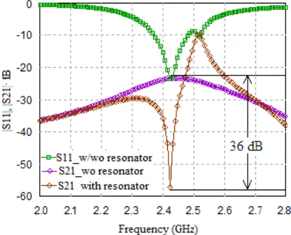
The direct mutual coupling between two patch elements can be canceled out by properly adding an extra indirect coupling path. A proper design aims at creating an indirect signal coming via the extra coupling path that opposes the signal going directly from element to element. If the two amplitudes are comparable, the two signals add up destructively and result is the considerably suppression of mutual coupling. As the mutual coupling is reduced between the patch elements, the occurrence of scan blind in the array integrated with the DGS is also suppressed. With the introduction of DGS, as shown in Figure 4, an extra coupling path can be created by properly adjusting the dimensions of the DGS cell. Here the DGS has been designed in such a way that it involves in the coupling at the resonant frequency of the patch elements. The dimension of the DGS cell has been optimized by the process of simulation. Simulated return loss and mutual coupling of the antenna structure with and without resonator are shown in Figure 5. The simulation process has been done by using IE3D electromagnetic simulator
Figure 4. Antenna structure with DGS cell
(indicated dimensions in millimeters) (λ =
122 mm).
Figure 5. Simulated S11 and S21 for antenna-1 with and without resonator.
based on the method of moment (MoM).
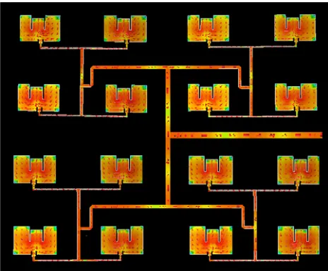
From Figure 5, it is observed that the mutual coupling is suppressed by 36 dB with the introduction of DGS between the antenna elements. This concept has been applied to a large array and accordingly, a sixteen-element array integrated with DGS cell has been designed as shown in Figure 6.
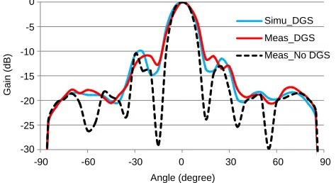
The simulated elevation pattern plots of sixteen-element array with and without DGS are shown in the Figure 7. It is observed that the scan blindness has been suppressed by 13.0 dBi with the introduction of the proposed DGS in the array structure.
The return loss characteristics of sixteen-element array is shown in Figure 8. It is observed that there is no significant change in return loss characteristics with the insertion of DGS cell. The simulated current distribution of the array antenna with DGSs at 2.45 GHz is shown in Figure 9. It is observed that all elements of the array are uniformly excited at the designed frequency. This is one of the ways to show the impedance matching of the array.
A 3D radiation pattern view of the proposed array with and without DGS is shown in Figure 10. The radiation in the horizontal direction is significantly suppressed as observed in comparing Figure 10(b) with Figure 10(a).
The sixteen-element array with and without DGS has been fabricated and measured. The fabricated
Figure 7. Simulated elevation pattern plot of sixteen-element array with and without DGS.
-25 -20 -15 -10 -5 0
2.2 2.3 2.4 2.5 2.6 2.7 2.8
|S
| dB
S _DGS
S _no DGS
11
11 11
Frequency (GHz)
Figure 8. Return loss of sixteen-element array with and without DGS.
Figure 9. Current distribution (with vector notation) of sixteen-elements array integrated with DGS.
(a) (b)
antenna structures are shown in Figure 11.
Measured elevation pattern gain of the sixteen-element array with DGS is shown in Figure 12. Here suppression of scan blindness of 13 dB has been observed in comparison to the array without DGS. The measured return losses with and without DGS is shown in Figure 13. It is observed that there is no significant change in the return loss characteristics of the array with and without DGS. From Figure 12, it is also observed that there is a small variation of the graphs of simulated and measured elevation patterns of the array with DGS at resonant frequency. This might be due to other unknown parasitic effects not considered in the simulation. Since the soldering is not done with a machine on the PCB, positional errors might give rise to the discrepancy.
Combined simulated and measured return loss characteristics of Figure 8 and Figure 13 are shown in Figure 14.
(a) (b) (c)
Figure 11. Fabricated array, (a) front view, (b) back view with DGS, and (c) back view without DGS.
-30 -25 -20 -15 -10 -5 0
-90 -60 -30 0 30 60 90
Gain (dB)
Angle (degree)
Simu_DGS
Meas_DGS
Meas_No DGS
Figure 12. Simulated elevation pattern plot of sixteen-elements array with and without DGS.
|S
| dB
Frequency (GHz) Measured_no DGS Measured_DGS
11
1.5 2 2.5 3 3.5
-25 -20 -15 -10 -5 0
Figure 13. Measured return loss with and without DGS.
2.2 2.3 2.4 2.5 2.6 2.7
Frequency (GHz) Measured_No dgs
Measured_dgs
Simulated_dgs
Simulated_No dgs -25
-20 -15 -10 -5 0
|S | dB 11
From Figure 14, it is observed that there is a small variation of simulated and measured return loss characteristics of the array at resonant frequency. This might be due to little mismatch of impedance of the fabricated array. As the number of antenna elements is large, the parasitic effects might give rise to the incongruity.
4. CONCLUSION
The aim of this work is to maintain the mutual coupling and scan blindness suppression with the designed structure as simple as possible while having a high amount of scan blindness reduction. This paper presents a novel structure suppressing the mutual coupling between nearby patches and scan blindness of the array. A dumbbell-shaped split-ring DGS is proposed as a technique of suppressing the radiation in the horizontal direction. An E-shaped patch array with and without resonator are examined using simulation and experimental results and the idea is verified. Furthermore, the dumbbell-shaped split-ring DGS causing suppression in mutual coupling does not affect other characteristics of the array. Thus, the proposed concept can be employed for achieving improved mutual coupling and radiation pattern with reduced scan blindness where high scan blindness becomes a major limitation in the array of antennas. Here mutual coupling of 36 dB between two antenna elements and scan blindness of around 13.0 dB have been suppressed.
REFERENCES
1. Pozar, D. M. and D. H. Schaubert, “Scan blindness in infinite phased arrays of printed dipoles,” IEEE Trans. Antennas Propag., Vol. 32, No. 6, 602–610, 1984.
2. Ghosh, C. K. and S. K. Parui, “Elimination of scan blindness of microstrip array by using I-shaped λ/2 resonator,”Microwave and Optical Technology Letters, Vol. 56, No. 2, 334–337, 2014.
3. Farsi, S., H. Aliakbarian, B. Nauwelaers, and G. A. E. Vandenbosch, “Mutual coupling reduction
between planar antenna by using a simple microstrip U-section,” IEEE Antennas and Wireless
Propagation Letters, Vol. 11, 1501–1503, Dec. 9, 2012.
4. Habashi, A., J. Nourinia, and C. Ghobadi, “Mutual coupling reduction between very closely spaced patch antennas using low-profile folded split-ring resonators,”IEEE Antennas and Wireless Propagation Letters, Vol. 10, 862–865, Aug. 22, 2011.
5. Nikolic, M. M., A. Djordjevic, and A. Nehorai, “Microstrip antennas with suppressed radiation in horizontal directions and reduced coupling,” IEEE Trans. Antennas Propag., Vol. 53, No. 11, 3469–3476, Nov. 2005.
6. Zhang, L., J. A. Castaneda, and N. G. Alexopoulos, “Scan blindness free phased array design using PBG materials,” IEEE Trans. Antennas Propag., Vol. 52, No. 8, 2000–2007, 2004.
7. Iluz, Z., R. Shavit, and R. Bauer, “Microstrip antenna phased array with electromagnetic band gap substrate,” IEEE Trans. Antennas Propag., Vol. 52, No. 6, 1446–1453, 2004.
8. Fu, Y. and N. Yuan, “Elimination of scan blindness in phased array of microstrip patches using electromagnetic band gap materials,” IEEE Antennas and Wireless Propagation letters, Vol. 3, 63–65, 2004.
9. Yang, F. and Y. R. Samii, “Microstrip antennas integrated with electromagnetic band-gap (EBG) structures: A low mutual coupling design for array applications,” IEEE Trans. Antennas Propag., Vol. 51, No. 10, 2936–2946, 2003.
10. Ghosh, C. K. and S. K. Parui, “Reduction of mutual coupling between E-shaped microstrip antenna array by using a simple microstrip I-section,” Microwave and Optical Technology Letters, Vol. 55, No. 11, 2544–2549, Nov. 2013.
11. Hou, D. B., S. Xiao, B.-Z. Wang, L. Jiang, J. Wang, and W. Hong, “Elimination of scan blindness
with compact defected ground structures in microstrip phased array,” IET Microw. Antennas
Propag., Vol. 3, No. 2, 269–275, 2009.