Generation and Mitigation of Common-Mode Noise for Differential
Traces with Adjacent Ground Line and a Ground Plane
Guang-Hwa Shiue1, *, Zhong-Yan You1, Yu-Hsiang Cheng1, Ting-Chun Wang2,
Kuang-Yi Wu1, Ming-Yuan Chuang2, and Chun-Fu Huang3
Abstract—This study investigates the generation and mitigation of common-mode noise (CMN) in a
common structure which consists of differential traces with adjacent ground lines and a ground plane. For simplicity, a simple test structure similar to the common structure is proposed. The test structure is divided into three parts. One part is composed of differential traces with adjacent ground lines. The second is composed of differential traces with adjacent ground lines that are connected to a ground plane. The third comprises differential traces with an adjacent ground line and an adjacent ground plane. The generation and mitigation of CMN in these three parts are studied. Test structures with different designs are investigated to confirm the effectiveness of the CMN mitigation schemes. Based on these analyses, design guidelines for mitigating CMN are provided. The proposed design guidelines reduce the peak-to-peak CMN amplitude by 81% from that achieved using unsuitable design of test structure. In the frequency domain, the reduction of the magnitude of differential-to-common mode conversion (|Scd21|) at the resonant peaks exceeded 40 dB in the frequency range 0 GHz ∼ 6 GHz. Finally, a comparison between simulated and measured results verifies the favorable CMN mitigation performance of the proposed design guidelines.
1. INTRODUCTION
Conventional high-speed digital circuits transmit signals by differential signaling [1]. Common applications include Serial Advanced Technology Attachment III (SATA III/6 Gbps), High Definition Multimedia Interface (HDMI/5 Gbps), PCI Express Interconnect III (8 Gbps), and USB 3.0 (5 Gbps) devices. The harmonic frequencies of high-speed digital circuits are in the tens of GHz. The advantages of using differential signals include improved signal integrity (SI), cancellation of electromagnetic interference (EMI), and immunity to noise [2]. However, an imbalance between differential signals and common mode noise (CMN) can worsen EMI problems by generating common mode current radiation that is transmitted through I/O cables [1, 3]. Therefore, a maximum common-mode voltage must be specified for high-speed GHz differential transmission systems such as USB 3.0. Recently, methods for mitigating CMN have been widely studied.
Interference by crosstalk noise severely degrades the performance of high-speed digital circuits when the noise increases the signal rise time. Such an interference is typically associated with near-end crosstalk (NEXT) and far-near-end crosstalk (FEXT) [4], both of which are proportional to mutual induction and capacitive coupling. However, FEXT is also proportional to the length of the coupled interconnects and is found only in inhomogeneous environments, such as microstrip structures. The transmission interconnects that are used in many current high-speed digital signal standards consist of
Received 26 March 2017, Accepted 7 June 2017, Scheduled 26 June 2017 * Corresponding author: Guang-Hwa Shiue ([email protected]).
1 Department of Electronic Engineering, Chung Yuan Christian University, Taoyuan City, Taiwan 32023, R.O.C.2Master Program
Figure 1. A practical and common routing scheme for I/O differential lines with ground structures (ground line and ground plane).
t 1Volt
r t
1 s
V
t
-1Volt
r t
2 s
V
(a)
(b)
Copper; 0.02
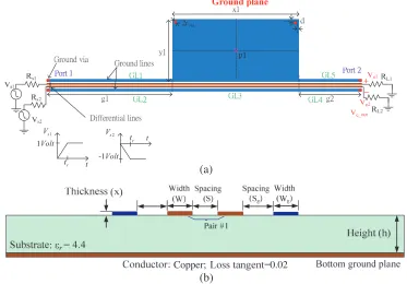
Figure 2. (a) Top and (b) cross-sectional views of test structure.
several differential line pairs. Additionally, owing to a high circuit routing density and a short rise time, the ground line (also called guard trace) and ground plane are generally placed between or adjacent to differential traces (Figure 1) to reduce crosstalk [5] and EMI. (Based on Figure 1, for simplicity, Figure 2 schematically depicts the differential traces with adjacent ground lines and a ground plane, which are together also called a test structure.
resonant frequency response. The typical solution is to increase the number of shorting vias to shift the first resonance frequency away from the bandwidth of interest [8]. In the time domain waveform, resonance is related to the spacing between shorting vias may generate large-amplitude ringing noise on the victim line, which is the main cause of FEXT on the guard trace [9].
High-speed data links depend on cables and connectors to transmit differential signals between various electronic devices or PCBs. Cables can cause EMI because CMN coupled to I/O cables or connectors causes them to act as antennas [3]. Therefore, an essential characteristic of state-of-the-art designs of electronic systems is the reduction of the CMN that is induced by differential interconnects. Figure 1 demonstrates that, in long I/O (input/output) differential lines in a practical and common PCB, crosstalk between differential traces is generally reduced by adding adjacent ground structures, such as a ground line (also called a guard trace) [5] or a ground plane. One end of the ground line is typically connected to a ground plane to maintain the zero voltage. The other end is connected to a bottom ground plane by a ground via. Figure 1 presents hardly any design guidelines that effectively mitigate CMN.
The generation and mitigation of CMN for differential traces with adjacent ground lines that are connected to a ground plane are simple to explain [10]. However, no clear design guidelines or measurements that pertain to the validation of the mitigation and generation of CMN are available. This investigation compares the generations and mitigations of CMN by three partial structures that are art of the test structure. Design guidelines for reducing CMN are also proposed. Validating measurements are made to confirm the generation and reduction of CMN.
The paper is organized as follows. Section 2 describes the problem and structure (test structure) of interest for differential traces with adjacent ground lines and a ground plane. Section 3 investigates the generation and mitigation of CMN in three structures that are separated from the test structure. In Section 4, the test structure is studied to verify the effectiveness of the CMN mitigation schemes. Section 4 also presents design guidelines for mitigating CMN. Section 5 compares simulated and measured results for verification purposes. Finally, Section 6 draws conclusions.
2. STRUCTURE AND PROBLEM
2.1. Structure
Figures 2(a) and 2(b) show top and cross-sectional views of the test structure along with relevant structural parameters, which are the trace width (W) of the differential lines, trace width (Wg) of the ground lines, trace spacing (S) of the differential traces, trace spacing (Sg) between the ground line and the differential traces, lengths (g1) of ground lines GL1 and GL2, length g2 of the ground lines GL4 and GL5, length (x1) of the ground line GL3, sizes x1 andy1 of the ground plane that is connected to the ground lines, height (h) of the substrate, dielectric constant (εr) of the substrate, thickness (x) of the signal trace, radius (rvia) of the ground vias, and distance (d) between the ground via and the side of the ground plane. Figure 2(a) also indicates that the ground vias are typically placed at the ends of the ground lines and at the two corners of the ground plane. Table 1 presents the related geometric dimensions and materials of the test structure that is shown in Figure 2. As illustrated by an example of a practical and common PCB (Figure 1), the design guidelines are usually unclear. In Figure 2, the driver and load resistances (Rs1, Rs2,RL1,RL2) are set to 50 Ω. Both driving sources, Vs1(t) and
Vs2(t), are ramp pulses with a magnitude of±1 V and rise time (tr) of 35 ps. The differential ramped
Table 1. Geometer dimensions and material parameters of test structures. (Figure 2).
x1 y1 W Wg Sg S h
18 mm 19 mm 4 mil 8 mil 6 mil 4 mil 4 mil
x rvia d g1 g2 εr loss tangent
step pulse (main signal) is propagated down the differential traces in all test cases that are described in Sections 3 and 4. To obtain precise data concerning the test structure, an HFSS [11] 3-D full-wave simulator is used for frequency-domain simulation, and CST [12] is used for time-domain simulation.
2.2. Statement of Problem
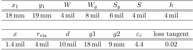
Figures 3(a) and 3(b) compare the time-domain CMN (Vc out) and simulated frequency-domain|Scd21| (differential-to-common mode conversion [13]) for the test structure. The common-mode voltage Vc out is defined as [3]
Vc out= Vo1+Vo2
2 (1)
where Vo1 and Vo2 represent the two voltages at the receiving ends of the differential traces. Figure 3 clearly demonstrates that CMN is high. High CMN that is carried to the I/O cables or connectors by differential traces generates considerable EMI [3]. Therefore, the following sections compare the generation and mitigation of three partial structures that are divided from the test structure. Design guidelines for reducing CMN are also proposed.
0 0.4 0.8 1.2 1.6
Time (ns)
-0.015 -0.01 -0.005 0 0.005 0.01
Vc
_
out
(V
o
lt)
test structure
0 4 8 12 16 20
Frequency (GHz)
-80 -60 -40 -20 0
|Scd
21
| (
d
B
)
test structure
(a) (b)
Figure 3. Simulated (a) time-domain CMN (Vc out) and (b) frequency-domain|Scd21|for test structure.
3. COMPARISON OF CMN GENERATION AND MITIGATION OF THREE PARTIAL STRUCTURES
A long open-stub ground line is typically connected to a ground plane in a multilayer package structure. The crosstalk that is induced by adjacent signal traces on the open-stub ground line then excites ground bounce noise between the pair of parallel ground planes [14]. The test structure (Figure 2) that is analyzed in this work includes a shorting-end ground line connected to a ground plane in the PCB structure. The objective is to determine whether crosstalk noise in a similar structure generates the CMN in differential traces.
To compare clearly the generation and mitigation of CMN, the test structure is divided in three parts. The first part consists of differential traces with adjacent ground lines (Section 3.1). The second part consists of differential traces with adjacent ground lines that are connected to a ground plane (Section 3.2). The third part is composed of differential traces with an adjacent ground line and an adjacent ground plane (Section 3.3). This section investigates CMN generation and mitigation in these three parts. Section 4 investigates the combined effects and design guidelines for mitigating CMN.
3.1. Differential Trace with Adjacent Ground Lines
(a) (b)
(c)
Figure 4. Three test cases: (a) TC A1, (b) TC A2, and (c) TC A3 concerning differential traces with
adjacent ground lines.
traces, in TC A2, a ground via additional to those used in TC A1 is placed at the center of GL1 (Figure 4(b)). In TC A5, a pair of symmetrical additional ground via s is placed on ground lines, so one additional ground via is placed at the center of GL1 and the other is placed at the center of GL2, as shown in Figure 4(c). Therefore, based on the placement of the additional ground via, the differential traces in TC A3 are not symmetrical whereas those in TC A1 and A2 are symmetrical.
Since TC A1 involves a microstrip structure, the differential traces induce far-end crosstalk and near-end crosstalk on two ground lines through mutual capacitance and inductance [2, 4]. However, since the ground lines are both shorting ends (ground vias), the near-end crosstalk is not generated on them. Therefore, the voltage on two ground lines is mostly far-end crosstalk that is induced from differential traces [10, 15]. The two propagating far-end crosstalks do indeed travel back and forth on their own ground line. According to crosstalk theory, the positive differential signal near GL1 and the negative differential signal near GL2 cause the propagating far-end crosstalks to become negative and positive, respectively. Therefore, since the structure (TC A1) is symmetric, the two far-end crosstalks exhibit reverse symmetry.
The two propagating far-end crosstalks on the own ground line can be regarded as other main signals that can induce other crosstalk noise (also called ringing noise [15]) on differential traces. Since the structure is symmetric and differential signals exhibit reversed symmetry, the other crosstalk noises on differential traces that are induced by two propagating far-end crosstalks exhibit reverse symmetry. Therefore, according to formula (1), the CMN (Vc1) at the receiving end of differential traces in TC A1 and TC A3 approaches zero, as shown in Figure 5(a). However, TC A2 is not symmetric, meaning that the sum of the two ground line voltages is not close to zero, and the CMN (Vc1) at the receiving end of the differential traces cannot approach zero, as shown in Figure 5(a).
Figure 5(b) shows the frequency-domain differential-to-common mode conversion|Scd21|. Notably, the ground line with two shorting ends forms a half-wavelength resonator. The resonant frequency of the half-wavelength resonator determines the length () of the ground line. The following equation yields the length of the half-wavelength resonance [16];
fr ≈n c
2√εr,e (2)
wherecis the speed of light in free space;εr,e is the effective dielectric constant of the ground line, and
0 0.2 0.4 0.6 0.8 1
Time (ns)
-0.006 -0.004 -0.002 0 0.002 0.004 0.006
V
ol
ta
g
e
(
V
ol
t)
Vc1
TC A1 TC A2 TC A3
0 4 8 12 16 20
Frequency (GHz)
-100 -80 -60 -40 -20 0
|S
cd
21
| (
d
B
)
TC A1 TC A2 TC A3
(a) (b)
Figure 5. Simulated time-domain voltages: ((a) Ground line voltages and (b) CMN (Vc1)) and (c)
frequency-domain|Scd21|in three cases (TC A1, TC A2, and TC A3) concerning differential traces with adjacent ground lines.
3.2. Differential Traces with Adjacent Ground Lines Connected to a Ground Plane
With reference to the test structure (Figure 2), Figure 6 shows the two test cases TC B1 and TC B2 that are compared in terms of CMN generation and mitigation for differential traces with adjacent ground lines that were connected to a ground plane. TC B1 (Figure 6(a)) is the case of CMN generation that is considered in this section. TC B2 (CMN mitigation) is the same as TC B1 except for the placement of an additional ground via on the connection between the ground line and the ground plane.
(a) (b)
Figure 6. (a) TC B1 and (b) TC B2 from the test structure (Figure 2), elucidating generation and
mitigation of CMN for differential traces with an adjacent ground line that is connected to a ground plane.
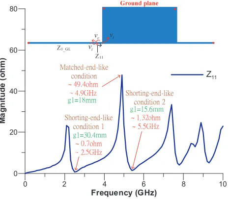
According to previous investigations [10, 14], the input impedance (Z11) (Figure 7) looking into the parallel ground planes from the connection between the ground line and the ground plane can be simulated using the HFSS. From the results in Figure 7, the impedances at two frequencies (2.5 GHz and 5.5 GHz) approach zero and that at one frequency point (4.9 GHz) approaches 50 Ω. Based on the conditions at three frequencies and formula (2), the lengths of the ground lines and the differential traces under shorting-end-like condition 1, matched-end-like condition, and shorting-end-like condition 2, are
gl = 30.4 mm, gl= 18 mm, and gl= 15.6 mm, respectively. The impedance of the connection between the ground line and the ground plane for gl = 30.4 mm and 15.6 mm satisfies the shorting-end-like condition and that for gl = 18 mm satisfies the matched-end-like condition. The relationship between the frequency-domain magnitudes of the voltage vt that is transmitted to the parallel ground planes can be simplified as [14]
vt(f)≈vi(f) 2Z11(f)
Z11(f) +Z0GL
(3)
Frequency (GHz)
0 20 40 60 80
Ma
g
n
it
u
d
e
(
o
h
m
)
Z11 i
v r
v vt
0 2 4 6 8 10
Figure 7. Simulated input impedance (Z11) look-ing into parallel ground planes from connection between ground line and ground plane.
0 0.4 0.8 1.2
Times (ns)
-0.004 -0.002 0 0.002 0.004
Voltage (
V
olt)
Vc1
TC B1 TC B2
Figure 8. Comparisons of simulated CMNs (Vc1)
for (a) TC B1 and (b) TC B2.
However, based on formula (3), an additional ground via at the connection between the ground line and one of the parallel ground planes (Figure 6(b)) can make Z11 approach zero for all frequencies [10, 14]. Then, the differential traces with GL1 and GL2 can be like those in TC A1.
Relative to TC A1 in Figure 4(a), TC B2 involves an additional ground via, so the induced CMN (Vc1) at the receiving end of differential traces is very small, as shown in Figure 8. The mitigation scheme also effectively prevents entry of the induced far-end crosstalk on the ground line into the parallel ground planes.
For the above reason, following the addition of an additional ground via at the connection between the ground line and one of the parallel ground planes, the mitigation scheme significantly reduces CMN for differential traces with adjacent ground lines that are connected to a ground plane.
3.3. Differential Traces with an Adjacent Ground Line and an Adjacent Ground Plane
This section compares the generation and mitigation of CMN in differential traces with an adjacent ground line and an adjacent ground plane. Based on the above test structure (Figure 2), Figure 9 shows the top views of three test cases, TC C1, TC C2, and TC C3. In TC C1, a ground via is added at the two ends of the ground line and the four corners of the ground plane. The lengths of the differential traces and the ground line equal the length (x1) of the long side of the ground plane. In TC C1, no
Ground plane
Vc2 GL3
0.33x1
0.66x1
(a) (b) (c)
Figure 9. Three test cases; (a) TC C1, (b) TC C2, and (c) TC C3, for differential traces with an
other additional ground via is present on the ground line or the ground plane. In TC C2, two additional ground vias are placed symmetrically on the ground plane and the ground line in the half (0.5x1) of GL3, as shown in Figure 12(b). In TC C3, two pairs of additional ground vias are placed symmetrically on the ground plane and the ground line at positions that are specified by 0.33 and 0.66 times the length of GL3, as shown in Figure 12(c).
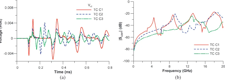
Figures 10(a) and 10(b) plot the simulated CMN (Vc2) and the differential-to-common mode conversion |Sc2d1|in three test cases, TC C1∼TC C3. The noise voltage induced by differential traces enters the ground planes from the side near the differential trace. The noise voltage spreads from the plane side to the ground planes. Therefore, the ground plane voltages near differential traces in TC C1∼C3 are all very small. Moreover, the ground line voltages of GL3 are all far-end crosstalk, whose amplitude is proportional to the length of the ground line and they generally exceed the ground plane voltages. Hence, the far-end crosstalk on GL3 becomes smaller as the number of pairs of symmetrically arranged additional ground vias increases. The difference between the ground plane edge voltage close to the differential trace and the ground line voltage is small, as is the CMN. Therefore, the CMN Vc1 and|Scd21|are largest in TC C1. The CMNVc1 and|Scd21|in TC C2 exceed those in TC C3 (Figure 10).
0 4 8 12 16 20
Frequency (GHz)
-100 -80 -60 -40 -20 0
|S
c2d
1
| (d
B)
TC C1 TC C2 TC C3
(a) (b)
Time (ns)
Figure 10. Comparisons of simulated (a) waveforms of ground line voltages and ground plane voltages,
(b)Vc2 and (c)|Scd21|in three test cases, TC C1, TC C2, and TC C3.
Adding pairs of symmetrical additional ground vias can shorten the ground line and yield a small ground line voltage, yielding a small CMN. Comparisons between Figures 5(b) and 10(b) reveal resonant frequencies that are determined by the length of the ground line in the frequency range of |Scd21|. Therefore, adding pairs of symmetrical additional ground vias for the differential traces that are adjacent to a ground line and a ground plane yields not only a little CMN but also a high first resonant frequency.
4. DESIGN GUIDELINES FOR MITIGATING CMN
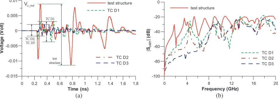
Based on the results obtained in Section 3, this section proposes design guidelines for mitigating CMN in the test structure (Figure 2). With reference to the test structure, Figure 11 shows three cases, TC D1∼TC D3, to validate the design guidelines for mitigating CMN. In TC D1 (Figure 11(a)), two pairs of ground vias are symmetrically added at the two connection positions between the ground plane and the ground lines. In contrast, in TC D2, two pairs of symmetrical ground vias are symmetrically added at the related 1/3x1 and 2/3x1 positions of GL3 and the side of the ground plane, as shown in Figure 11(b). In contrast again, in TC D3 (Figure 1(c)), only one pair of ground vias is symmetrically added at the center of GL1/GL2. The simulated results for the test structure (Figure 2) are compared with those for TC D1∼TC D3. Figure 12 compares the simulated differential-to-common mode conversions (|Scd21|) and CMN values (Vc out) of differential traces in the four cases (test structure and TC D1∼TC D3).
(a) (b)
(c)
Figure 11. Three test cases ((a) TC D1, (b) TC D2, and (c) TC D3) that are utilized to study design
guidelines for mitigating CMN.
0 0.2 0.4 0.6 0.8 1 1.2 1.4 1.6 1.8
Time (ns)
-0.015 -0.01 -0.005 0 0.005 0.01
Vol
ta
g
e
(
V
ol
t)
test structure
TC D1
TC D2 TC D3
0 4 8 12 16 20
Frequency (GHz)
-100 -80 -60 -40 -20 0
TC D1 TC D2 TC D3 test structure
(a) (b)
Figure 12. Comparisons of simulated (a) differential-to-common mode conversions (|Scd21|) and (b)
Vc outvalues of differential traces in four test cases (test structure and TC D1∼TC D3).
traces have an asymmetrical structure, so the CMN of the structure is high (Figure 12). In Figure 12, a comparison of the test structure clearly reveals that the peak-to-peak value of CMN (Vc out) and the mean magnitude of |Scd21| in TC D1 are significantly mitigated. Section 3.1 investigates the CMN mitigation scheme in case TC A1, whereas Section 3.2 investigates it in case TC B2. The reduction of TC D1 from that obtained using the test structure is almost 54%. In the frequency domain, the mean magnitude of |Scd21| in TC D1 is much smaller than that in the test structure in the frequency range 0∼4.5 GHz (Figure 12(b)).
D3, the first resonant frequency is increased from 4.5 GHz to 6 GHz (Figure 12(b)). The EMI effect in the range 0∼9 GHz in TC D3 is weaker than those in other cases.
The peak-to-peak value of CMN in TC D3 is almost 81% lower than that obtained using the test structure. CMN mitigation schemes significantly reduce the time-domain CMN ratio. Comparisons in the frequency domain demonstrate that CMN mitigation schemes can reduce the magnitude of |Scd21| (Figure 12(b)) at the resonant peaks by more than 40 dB in the frequency range 0 GHz∼6 GHz.
Based on the above results, the following design guidelines are proposed for mitigating CMN in differential traces with adjacent ground lines and an adjacent ground plane ((test structure (Figure 2)). (1). One pair of symmetrical additional ground vias must be added at the connection between the ground line and the ground plane. (2). For the differential traces adjacent to one ground line and the one ground plane, adding pairs of symmetrical additional ground vias at symmetrical and average positions of the ground line and the side of the adjacent ground plane can mitigate CMN. (3). The differential traces with adjacent ground lines must maintain symmetry. Restated, pairs of ground vias for differential traces adjacent to ground lines must be symmetrically added. (4). To obtain low EMI at low frequency range, more pairs of symmetrical additional ground vias must be added to the ground structure adjacent to differential traces.
5. MEASUREMENT VALIDATION
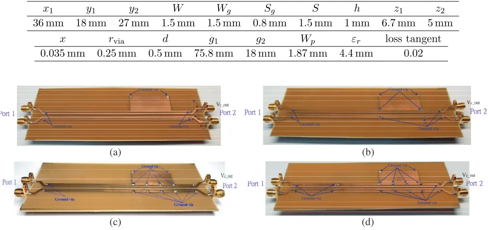
The effectiveness in CMN mitigation of the proposed design guidelines for differential traces with adjacent ground lines and an adjacent ground plane in a common microstrip structure was evaluated by comparing simulated results with measurements in both frequency and time domains. To make a clear comparison, the mitigation of CMN was measured in four boards that were designed for the purpose: (1) measured board 1 (similar to test structure), (2) measured board 2 (similar to TC D1), (3) measured board 3 (similar to TC D2), and (4) measured board 4 (similar to TC D3). Measured board 1 and measured board 2∼4 provide the CMN generation and mitigation conditions, respectively. For ease of implementation, the boards on which measurements are made are fabricated at the mm-scale. Table 2 presents the parameters that are related to the geometric dimensions and the materials of the boards of which measurements are made. Figure 13 shows photographs of those boards.
Table 2. Dimensions and material parameters of measured boards.
x1 y1 y2 W Wg Sg S h z1 z2
36 mm 18 mm 27 mm 1.5 mm 1.5 mm 0.8 mm 1.5 mm 1 mm 6.7 mm 5 mm
x rvia d g1 g2 Wp εr loss tangent
0.035 mm 0.25 mm 0.5 mm 75.8 mm 18 mm 1.87 mm 4.4 mm 0.02
(a) (b)
(c) (d)
Figure 13. Photographs of four boards of which measurements are made; (a) board 1, (b) board 2 (c)
The results in the time- and frequency-domains of the simulations of the two structures of which measurements are made are obtained using the 3-D full-wave simulator CST and HFSS, respectively. A time-domain reflectometer TEK/CSA8000 and a frequency-domain network analyzer Agilent/E5071B are used to perform an experimental comparison of the results of the CST and HFSS simulations. The launching voltage source is drawn from the reflectometer in the CST simulation.
Figure 14 plots the simulated and measured differential-to-common mode conversions (|Sc2d1|) and time-domain CMN (Vc out) for the four boards. All simulation results are highly consistent with the measurements. The deviations between the simulation results and the measurements are attributable to various factors, including the measured coaxial cables and the connectors that are used in the simulations, small variations in the material properties of the substrate, and small variations in the manufacturing processes. Despite the slight discrepancies, both simulations and measurements clearly confirm the feasibility and usefulness of the proposed analysis and design guidelines for mitigating CMN.
Measured bo ard 1
Measurement Simulation
0 1 2 3 4 5
Time (ns) -0.01 -0.005 0 0.005 0.01 Voltage ( V olt)
Measured board 2
Measurement Simulation
0 1 2 3 4 5 Time (ns) -0.01 -0.005 0 0.005 0.01
Measured board 3
Measurement Simulation
0 2 4 6 8 10
Frequency (GHz) -80 -60 -40 -20 0 |S cd 21 |( d B )
Measured board 1
Measurement Simulation
Measured board 4
Measurement Simulation |S cd 21 |( d B ) (a) (b) (c) (d) Frequency (GHz)
Figure 14. Simulated and measured (a), (b) time-domain CMN (Vc out) and (c), (d) frequency-domain
differential-to-common mode conversion (|Scd21|) for four boards.
6. CONCLUSIONS
adjacent to one ground line and one ground plane. The generation and mitigation of CMN in the three structures were investigated. Then, different designs of the test structure were compared to confirm the effectiveness of the CMN mitigation schemes. Based on the investigations and comparisons herein, design guidelines for mitigating CMN in differential traces with adjacent ground lines and an adjacent ground plane are proposed. The peak-to-peak CMN amplitude of using the proposed design guidelines was about 81% of that achieved using a poor design. Further comparisons in the frequency domain demonstrated that CMN mitigation in the magnitude of differential-to-common mode conversion (|Scd21|) at the resonant peaks exceeded 40 dB in the frequency range 0 GHz∼6 GHz.
Finally, a favorable comparison between simulation results and measurements convincingly demonstrated the effectiveness of the proposed design guidelines for mitigating CMN for differential traces with adjacent ground lines and an adjacent ground plane.
ACKNOWLEDGMENT
The authors would like to thank NTUEE SI Laboratory, Allied Circuit Co., Ltd., and Ansys Taiwan, for providing measurement equipment and simulation software. This work was supported by the National Science Council, Republic of China, Taiwan, under Grant NSC 103-2221-E-033-009.
REFERENCES
1. Fan, J., X. Ye, J. Kim, B. Archambeault, and A. Orlandi, “Signal integrity design for high-speed digital circuits: Progress and directions,” IEEE Trans. Electromagn. Compat., Vol. 52, No. 2, 392–400, May 2010.
2. Bogatin, E., Signal Integrity-simplified, Prentice Hall Modern Semiconductor Design Series’ Sub Series: PH Signal Integrity Library, 2003.
3. Paul, C. R., Introduction to Electromagnetic Compatibility, 2nd Edition, Wiley, New York, 2006. 4. Paul, C. R., “Solution of the transmission-line equations under the weak-coupling assumption,”
IEEE Trans. Electromagn. Compat., Vol. 44, No. 3, 413–423, Aug. 2002
5. Mbairi, F. D., W. P. Siebert, and H. Hesselbom, “On the problem of using guard traces for high frequency differential lines crosstalk reduction,” IEEE Trans. Comp. and Packag. Tech., Vol. 30, No. 1, 67–74, Apr. 2009.
6. Ladd, D. N. and G. I. Costache, “SPICE simulation used to characterize the cross-talk reduction effect of additional tracks grounded with vias on printed circuit boards,” IEEE Trans. Circuits Syst. II, Vol. 39, 342–347, Jun. 1992.
7. Novak, I., B. Eged, and L. Hatvani, “Measurement by vector-network analyzer and simulation of crosstalk reduction on printed circuitboards with additional center traces,” Instrumentation Measurement Technol. Conf., 269–274, Irvine, CA, May 1993.
8. Suntives, A., A. Khajooeizadeh, and R. Abhari, “Using via fences for crosstalk reduction in PCB circuits,”2006 IEEE Int. Symp. Electromagnetic Compat., 34–37, Portand, Orgeon, USA, Aug. 14– 18, 2006.
9. Cheng, Y. S., W. D. Guo, G. H. Shiue, H. H. Cheng, C. C. Wang, and R. B. Wu, “Fewest vias design for microstrip guard trace by using overlying dielectric,” 2008 IEEE-EPEP, 321–324, San Jose, CA, Oct. 27–29, 2008.
10. Hung, H. C., S. L. Hong, K. S. A. Chou, Z. X. Chen, C. H. Ting, S. C. Hsu, L. C. Chen, and G. H. Shiue, “Common-mode noise effect for differential traces adjacent ground lines connection a ground plane,” 2015 Asia-Pacific Symp. Electromagnetic Compat., 502–505, Taipei, Taiwan, R.O.C., May 26–29, 2015.
11. Ansys HFSS, ver. 13, Ansys, Pittsburgh, PA, [Online], Available: www.ansys.com.
12. CST Microwave Studio, Manual Computer Simulation Technology, Germany, 2003, Online, Available: www.cst.com.
14. Shiue, G. H., C. L. Yeh, P. W. Huang, H. Y. Liao, and Z. H. Zhang, “Ground bounce noise induced by crosstalk noise for two parallel ground planes with a narrow open-stub line and adjacent signal traces in multilayer package structure,” IEEE Trans. Comp. and Packag. Tech., Vol. 00, 2014. 15. Cheng, Y. S., W. D. Guo, C. P. Hung, R. B. Wu, and D. D. Zutter, “Enhanced microstrip guard
trace for ringing noise suppression using a dielectric superstrate,” IEEE Trans. Adv. Packag., Vol. 33, No. 4, 961–968, Nov. 2010.