Pandian Saraswathi Yadav Engineering College, Arasanoor, Sivagangai, Tamilnadu, India
A Precision Transconductance for Electrical
Impedance Tomography Using CMOS
Technology
M.Mohanaselvi
1, P.Maheswari
2PG Scholar, M.E.VLSI DESIGN, Sri Vidya College of Engineering & Technology, Tamilnadu, India1
Assistant Professor, Department of ECE, Sri Vidya College of Engineering & Technology Tamilnadu, India2
ABSTRACT: Current Drivers are suitable for bioimpedance measurements applications.The CMOS current driver circuits are portable for high resolution, high frequency image system.Current driver are require accurate output current value.This current driver circuits are introduced based on a transconductance and provide accurate current output.This circuit design uses multithreshold CMOS technology (MTCMOS) and negative feedback.The circuit was fabricated in a 0.22µm MTCMOS process technology.It operates at 5v power supply and it can deliver the output current 5mA.
KEYWORDS: CMOS current driver; Transconductance; bioimpedance; Electrical impedance tomography (EIT); Multithreshold CMOS technology.
I. INTRODUCTION
ELECTRICAL IMPEDANCE TOMOGRAPHY (EIT) is a new medical imaging technique.These system offers a non-invasive,low cost medical image approach [1][16].Most bioimpedance measurement techniques are particular interest in EIT.Current patterns are applying to the body surface through electrodes and measure the resulting voltage.A complete set of impedance measurement may be reconstructed into tomographical image [12].Some EIT system use multifrequency to get better differentiation between normal and abnormal tissue within the same organ [2][13]. Current driver are the fundamental circuit in EIT system. These circuits are suitable for bioimpedance application. Current driver is used to control the circuit such as high power transistor.They are usually used to regulate the current flowing through a circuit or are used to control the other factors such as other component, some device in the circuits. These circuits to provide accurate output current to the tissue load [2][9].Current driver circuits have three stages there are preamplifier, transconductance, voltage buffer. This circuit design uses differential amplifier and negative feedback.Here using multifrequency operation in transconductance stage so it consumes more power. The main limitation of this current driver is the upper frequency operation limits by the delay present at high frequency and it consumes more power [1][14].
Considerable effort has been made to reduce or even eliminate this limitation, first to develop a current driver circuit uses negative feedback and multithreshold CMOS technology. This paper presents a current driver based on transconductance stage.The second objective is to modify the transconductance stage using MTCMOS.To optimizes power consumption and it provides maximum output current accuracy. This paper is an expansion of [1] and presents the complete design and simulation results of current driver in 0.22-µm Multithreshold CMOS technology. This paper organized as follows.Section II outlines the system architecture and operation of current driver.Section III describes the circuit design.Section IV present simulation results of current driver.The concluding remarks of Section V complete the paper.
II .RELATED WORK
driver design uses nonlinear feedback and it provides outputs with low phase error.This circuit more suitable for high frequency integrated circuit applications.The drawback of this system is multifrequency currents can generated only each individual frequency phase is corrected [2][17].
Hong.s,Lee.K,Ha.U,Kim.H proposed the paper “A 4.9m ohm Sensitivity Mobile EIT IC for early Breast Cancer Detection System”describes about the mobile EIT IC is proposed for early breast cancer detection personally at home.This system design by Differential sinusoidal current source and it support three operating mode gain scanning, contact impedance monitoring, and EIT modes for the clear EIT image.The main drawback of this system is achieve high output impedance it suffers from a high common mode voltage error appearing across the load [3].
Marco Guermandi,R cardu,R Guerrieri proposed the paper “Active Electrode IC for EEG&EIT with continuous monitoring of contact impedance”describes about the IC is designed to acquire EEG and EIT signals at the same time so as to have the best possible integration between the two techniques.This overcomes the common limitations associated with using two separate systems for EEG and EIT.This system electrode able to program at any time and it improve the output signal quality.The main drawback of this system is suffer from low spatial resolution [4][18].Gustavo sato dos santos,Simon Arridge,David Holder proposed the“Multifrequency Electrical Impedance Tomography using Spactral Constraints”describes about the Multifrequency electrical impedance tomography(MFEIT) the dependence of tissue impedance on frequency to recover an image of conductivity.This system provides emergency diagnosis of pathologies such as acute stroke, brain injury and breast cancer.The main drawback is conductivity image is not possible[5][20].
Sntos.S.A,Leonhardt S proposed the“ Simulation of a Current Source with a Cole-Cole for Multifrequency EIT”describes the accurate current source is one of the keys in the hardware of Electrical impedance Tomography systems.This system design uses improve Howload current source and it provides a constant and stable output current.Limitations appear at high frequencies operations[9].Aaron S,Tucker,Robert M.Fox,Rosalind J.Sadleir proposed the“Biocompatible,high precision,wideband,Improved howload current source with Lead-leg compensation”describes the bioelectrical circuit is deliver precise electrical currents.This paper is improved current driver based on a pair of balanced operational transconductance amplifiers using a negative feedback loop.The drawback of this system is output impedance of the Howland is a critical figure of merit that limits the precision of the delivered current when the load changes[10].
III. SYSTEM ARCHITECTURE
Figure.1 shows the block diagram of the current driver.It consists of three major building blocks; preamplifier, transconductance, voltage buffer. Current driver design by using negative feedback and MTCMOS.The use of negative feedback therefore reduces input source error and circuit should be stable and also it enhances the circuit output current.Multithreshold CMOS uses in the transconductance stage it optimize power consumption.
Pandian Saraswathi Yadav Engineering College, Arasanoor, Sivagangai, Tamilnadu, India
A .Preamplifier
The preamplifier circuit is use to improve the small electric signal strength. These circuit are designed by cascode current mirror [1].It used to boost the signal strength to drive the cable to the main circuit without significant degrading the signal to noise (SNR).
B. Transconductance
The transconductance circuit is designed based on multithreshold CMOS technology.The use of MTCMOS is optimize the power consumption.These circuit acts as a port to transmit input signal from input source to output side without voltage drop.Their purpose is enhance output current and signal gain value.
C. Voltage Buffer
The voltage buffer circuit design by using intersection of inverter. These circuit uses to measure the output voltage. Voltage buffer output is fed into preamplifier negative input terminal it forms the negative feedback path. This path is optimizing accruing noise in this circuit.
IV. CIRCUIT DESIGN
A .Preamplifier
Figure.2 shows the schematic diagram of the preamplifier. These circuit is often placed closed to the input source it reduce the effect of noise and interference.
Fig.2 schematic diagram of preamplifier
B. Transconductance
Figure.3 shows the schematic diagram of the transconductance.Input current source is applied to the M15-M17 of the transistors in this circuits.In this transconductance stage is important part of the current driver system.Preamplifier output voltage is fed into transconductance input v2 terminal.Operation of this circuit is to transmit the input source from input terminal to output source without any signal drop.In conventional circuit consume more power in this stage.So we use multitheshold CMOS technology in proposed current driver circuits.This technology which has transistor with multiple threshold voltage it optimize power and delay.
Fig.4 schematic diagram of voltage buffer
Creating device with multiple threshold voltage is to apply different bias voltage to the base terminal of the transistor. In this circuit apply different bias voltage to the transistors. These circuits have large number of transistor in a current driver, the grater gain it is capable of delivering which all other factor constant. It has directly control the current through the circuit.Their purpose is produce high output impedance, current maintain at constant and enhance the gain. Current driver require high output impedance and stable current to the output. These circuit used regulate and set the voltage it produce constant output.
Pandian Saraswathi Yadav Engineering College, Arasanoor, Sivagangai, Tamilnadu, India
C. Voltage buffer
Figure.4 shows the schematic diagram of the voltage buffer.This circuit design by using CMOS inverter.These circuit uses four inverters.Inverter are (M1-M2)(M3-M4) (M5-M6)(M7-M8).Inveter1,2 connected in serial and 3,4 also connected in serial.
A voltage buffer is used to transfer a voltage from a first circuit, having a high output impedance level, to a second circuit with a low input impedance level. The interposed buffer amplifier prevents the second circuit from loading the first circuit unacceptably and interfering with its desired operation.
Transconductance M14,M15 transistor input fed into voltage buffer(M1-M2)(M3-M4) inverter input terminals.These circuit operates with very low power loss and at relatively high speed.Output voltage are measured by this circuit.Their purpose is provides short transmission time and low power consumption.
V. MEASUREMENT AND RESULT
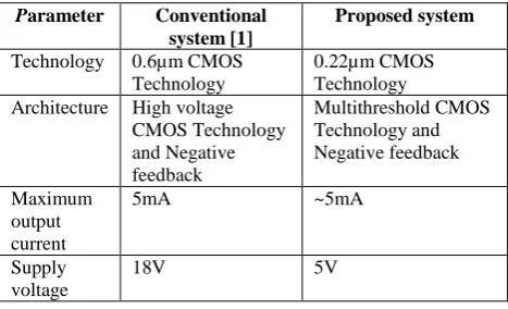
The proposed current driver with MTCMOS technology show in Figure.5 was designed in 0.22-µm CMOS technology.From the experimental results shows in table.1, the input voltage of conventional is 18v, then the input voltage of proposed current driver is 5v and output voltage is 5v.
Parameter Conventional system [1]
Proposed system
Technology 0.6µm CMOS Technology
0.22µm CMOS Technology Architecture High voltage
CMOS Technology and Negative feedback
Multithreshold CMOS Technology and Negative feedback
Maximum output current
5mA ~5mA
Supply voltage
18V 5V
Table 1.comparison table between conventional and proposed system
Fig.5 Schematic diagram of current driver
VI. CONCLUSION
In this paper, we designed and simulate the current driver with Multithreshold CMOS to achieve accurate output current and low power consumption.We concentrated on the output current accuracy is increase and reduces power consumption compare with a conventional system.For this design of CMOS current driver in CMOS design methodology we used Tanner EDA 15.11 simulation tool.
REFERENCES
[1] L. Constantinou, I. F. Triantis, R. Bayford, and A. Demosthenous,“High-power CMOS current driver with accurate Transconductance for electrical impedance tomography,” IEEE Trans. Biomed. Circuits Syst., vol. 8, no. 4, pp.575–583,Aug.2014
[2] Andres Demosthenous, Peter J.Langlois “A Sinusoidal Current Driver with an Extended Frequency Range and Multi frequency Operation for Bioimpedance Application’’ IEEE Transaction, June2014
[3] Hong.s, Lee.K, Ha.u, Kim.H “A 4.9mohm Sensitivity Mobile EIT IC for Early Breast cancer Detection System” IEEE Journal,September2014
[4] Marco Guermandi, R cardu, R Guerrieri “Active Electrode IC for EEG&EIT with continuous monitoring of contact
impedance”IEEETransaction,May2014
[5] Gustavo Sato dos Santos, David Holder, and Simon Arridge “Multifrequency Electrical Impedance Tomography Using Spectral Constraints”IEEETransaction,March2014 . [6] Vidya Sarode, Hema Patil, Alice N. Cheeran “Lab VIEW based Automatic Data acquisition system for Electrical ImpedanceTomography”IJCSIT,2014
[8] Nan Li, Hui Xu, Zhou Zhou, Jinling Xin, Zhaolin Sun, Xin Xu “Reconfigurable Bioimpedance Emulation System for Electrical Impedance Tomography System Validation” IEEE Transaction,June2013
[9] Santos S.A, Leonhardt S “Simulation of a Current Sourcewith a Cole-Cole For Multi frequency EIT”IEEE Transaction, July2013 [10] Aaron S. Tucker, Robert M.Fox, Rosalind J.Sadleir “Biocompatible, High Precision, Wideband, Improved Howland Current Source with
Lead-Lag Compensation”IEEE Transaction, March2013 [11] A. S. Tucker, R. M. Fox, and R. J. Sadleir, “Biocompatible, high precision,wideband, improved Howland current source with lead-lag
compensation,”IEEE Trans. Biomed. Circuits Syst., vol.7,no.1,pp.63-70,2013 [12] J. C. Baeg, H. Wi, T. I. Oh, A. L. McEwan, and E. J. Woo, “An amplitude-to-time conversion technique for multichannel data acquisitionand bioimpedance imaging,” IEEE Trans. Biomed Circuits Syst., vol.7, no. 3, pp. 349–354, 2013.
[13] R. Bayford, P. Kantartzis, A. Tizzard, R. Yerworth, P. Liatsis, and A.Demosthenous, “Development of a neonate lung reconstruction algorithmusing a wavelet AMG and estimated boundary form,” Physiol.Meas., vol. 29, pp. 125–138, 2008.
[14] L. Constantinou, A. Demosthenous, P. Langlois, R. Bayford, and I.Triantis, “An improved CMOS current driver for electrical impedance tomography,” in Proc. 20th Eur. Conf. Circuit Theory and Design,Linköping, Sweden, 2011, pp. 290–293.
[15] R. Bayford and A. Tizzard, “Bioimpedance imaging: An overviewof potential clinical applications,” Analyst, vol. 137, pp. 4635–4643,2012. [16] B.H.Brown, R. A. Primhak, R. H. Smallwood, P. Milnes, A. J.Narracott,and M. J. Jackson, “Neonatal lungs: Can absolute lung resistivity be
determined non-invasively,” Med. Biol. Eng.Comput., vol. 40, pp.388–394, 2002
Pandian Saraswathi Yadav Engineering College, Arasanoor, Sivagangai, Tamilnadu, India
Arridge, E. M. C. Hillman, and A. G. Yodh, “Diffuse optical tomography with spectral constraints and wavelength optimization,” Appl. Opt., vol. 44,no. 11, pp. 2082–93, Apr. 2005.
[20] A. McEwan, A. Romsauerova, R. Yerworth, L. Horesh, R. Bayford, and D. S. Holder, “Design and calibration of a compact multi-frequency