ABSTRACT
DUEWER, BRUCE ELIOT. A Low-Power, High Performance MEMS-based Switch Fabric. (Under the direction of Paul D. Franzon.)
A LOW-POWER, HIGH PERFORMANCE MEMS-BASED SWITCH FABRIC
by
BRUCE ELIOT DUEWER
A dissertation submitted to the Graduate Faculty of North Carolina State University
in partial fulfillment of the requirements for the Degree of
Doctor of Philosophy
COMPUTER ENGINEERING
Raleigh 2001
APPROVED BY
______________________________ _____________________________
BIOGRAPHY
Bruce Duewer, son of Lawrence and Elaine Duewer, was born on August 21, 1973 in Fairfax, Virginia. He has a younger brother, Trent, and sister, Rachel. He graduated from the Thomas Jefferson High School for Science and Tech-nology in 1991, and became an Eagle Scout the same year. In 1995 he received a BS from Virginia Tech, with a double major in Electrical Engineering and Computer Engineering, and a minor in Computer Science. In 1996 he received a MS in Computer Engineering at North Carolina State University.
ACKNOWLEDGEMENTS
I would like to thank Dr. Paul Franzon for his service help and guidance through my time at NCSU. I appreciate how despite an incredibly busy sched-ule, he always made time when I needed to discuss something with him, yet was patient with the various delays and challenges I encountered with the project, and made sure I had the resources necessary to explore solutions. I’d like to also thank the rest of my committee for their support and advice: Dr. Thomas Conte, Dr. Wentai Liu, and Dr. Jacqueline Krim. Also, Dr. Clay Gloster for serving on my committee until he moved out of the state.
David Winick taught me a lot about MEMS, and was a lot of help through-out the project. He helped me scale the learning curves involved in moving from the fairly unrelated areas that had been my focuses in earlier degrees to mechanical design. He also prepared and maintained much of the infrastruc-ture for design and testing of MEMS here, adapting the tools (for example, he wrote an excellent script for cross section extraction that I used extensively), and in specifying and assembling the test equipment we used. We worked together on the bistability for array addressability scheme, which provided the foundation for much of what I developed.
Alan Glaser and Toby Schaffer also provided a lot of help with the design tools, particularly in the design of simulation of electronic circuits.
driver stage of the control chip. He and Steve Lipa helped a lot with high fre-quency testing, and with my understanding of high frefre-quency testing issues and test structures. The circuit model for a bank of MUMPS devices discussed in section 3.7 was developed by John Wilson (my earlier models had only resis-tance and capaciresis-tance components), and he did the fitting of component values with the test data.
David Nackashi, Andrew E. Oberhofer, and Jeff Chang all helped me in the cleanroom, preforming the evaporation depositions. JMC Tool & Machine manufactured the steel mounts for the evaporator. David Nackashi and John Damiano provided advice on process issues involved with metallization.
I’d like to thank all my fellow ERL students. They are very talented bunch, good people to either share an office or go rock climbing with.
TABLE OF CONTENTS
Page
LIST OF TABLES ix
LIST OF FIGURES x
Chapter 1. Introduction 1
1.1 Motivation 1
1.2 Goals 2
1.3 Overall Approach 2
1.4 Crossbar Scaling 3
1.5 Thin Film MEMS 4
1.6 Challenges & Novel Contributions 6
1.7 Target Crosspoint 8
1.8 Outline of Dissertation 9
Chapter 2. Literature Review 11
2.1 Architectural Issues 11
2.1.1 Switching Networks 12
2.1.2 Clos Networks 13
2.1.3 Programming Clos Networks 16
2.2 Circuit Issues 19
2.2.1 Other crossbars 20
2.2.2 Resistors 20
2.2.3 Automated Bias Control (ABC) Circuit 23
2.2.4 Optical Receiver 25
2.2.5 Quantized Feedback 29
2.2.6 Conclusions Regarding Signaling 31
2.2.7 High Voltage Generation 31
2.3 Device Design 32
2.3.1 Silicon as a Mechanical Material 32
2.3.2 Micromachined Relays 33
2.3.3 Spring Design 34
2.3.4 A Previous Bistable Device 36
2.3.5 An RF and Microwave device 37
Chapter 3. Device Operation & MUMPs 39
3.2 Bistability & Array Addressing 41
3.2.1 Derivation of Bistability 42
3.2.2 Array Addressability 44
3.2.3 Stop Gap Height Implications on Bistability 45 3.2.4 Device Throw Implications For Bistability 47
3.2.5 Requirements For Addressibility 47
3.2.6 Experimental Confirmation of Bistability 48
3.2.7 Experiment Details 50
3.3 Substrate Effects on Actuation 53
3.4 MUMPs Designs 55
3.4.1 MUMPs 14 and 18 55
3.4.2 MUMPs 20 58
3.4.3 Later MUMPs runs 60
3.5 Modeling 61
3.5.1 Matlab 61
3.5.2 FastCap 63
3.5.3 MEMCAD 63
3.6 S-parameter results for example device 65
3.7 S-parameter results for a bank of devices 67 Chapter 4. Design of MEMS Structures for Packaging and Test 69
4.1 Introduction 69
4.2 Basic Thin Film MEMS Design Concerns 69
4.3 Electrical Modeling of MEMS Structures 72
4.4 Transmission lines in MUMPs 74
4.5 Testing Considerations: Probing 77
4.5.1 Design for Probing 77
4.5.2 Probe Specifics 78
4.5.3 Two example probe stations 80
4.5.4 Modeling of probing 81
4.5.5 Doing the probing 82
4.6 Packaging 84
4.7 Conclusions 85
Chapter 5. MEMS Crossbar Architecture 86
5.1 System Description 86
5.2 Crossbar Architecture Selection 88
5.3 Characteristics Of A Direct Implementation 89
5.4 Size Limitations 89
5.5 Clos Array Sizes Selection 90
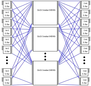
5.7 The System 96
5.8 Signal Path 97
5.9 Overall Power Consumption 100
Chapter 6. Metallization 101
6.1 Metallization Options 101
6.2 Layout for Metallization 102
6.2.1 Mechanical Concerns 104
6.2.2 Low Resistance Line Crossings 104
6.3 Metallization (Sputtering): First SUMMiT Run 107
6.3.1 Visual Inspection 107
6.3.2 Electrical & SEM Tests 110
6.4 New Metallization Test Structures 113
6.5 Metallization(Sputtering): Second SUMMiT Run 114 6.5.1 Metallization Test Structure Testing 115
6.5.2 “Bubbling” and the SAM 117
6.6 Metallization of chips from no-SAM release 119 6.6.2 Some Probing Abnormalities Explained 121
6.6.3 Testing 122
6.7 Evaporation 123
6.7.1 Evaporator Geometry 123
6.7.2 Synthetic Spread Angle 124
6.7.3 Initial Sanity Check 127
6.7.4 First Four Depositions 128
6.7.5 Another Evaporation Run 130
Chapter 7. Devices Using SUMMiT 132
7.1 SUMMiT Process Features Relative to MUMPs 132
7.2 Initial Planning 133
7.3 Rule Adjustments 134
7.4 Some Basic Design Trade-offs 137
7.5 Device Design 138
7.5.1 Design to Survive metallization 140
7.6 The First SUMMiT Run 141
7.6.1 Devices Included 141
7.6.2 Test Results 145
7.7 Second SUMMiT Run 146
7.7.1 Devices Included 146
7.7.2 Test Results: Sputtering 147
7.7.3 Test Results: Evaporation 149
7.9 Capacitance Ratio 151
Chapter 8. Conclusions & Future Work 154
8.1 Achievements 154
8.2 Remainders 155
8.3 Changes 155
8.4 Directions for Future Work 156
References 158
Apprendix 1. Equation Derivations 163
Apprendix 2. Program Listings & Outputs 169
2.1 Clos Array Combination Generator 169
2.2 Clos Programing Code 170
LIST OF TABLES
Page
Table 1 Control for Figure 9 Devices 50
Table 2 Control Voltages 51
Table 3 HighVolt Logic 94
LIST OF FIGURES
Page
Figure 1 Signal Path 3
Figure 2 MUMPs Release Example. Source [39] 5
Figure 3 Resistor Circuit 21
Figure 4 Auto Bias Circuit 24
Figure 5 Restoration of Signal 29
Figure 6 Individual MEMS switch 40
Figure 7 Voltage-Displacement Characteristic (flat plate model) 42
Figure 8 Array Addressing Scheme. 45
Figure 9 Microphotographs demonstrating array addressability. The vertical springs for the ‘down’ switches show fringe lines. 49 Figure 10 Substrate Effects on Pull-in and Release voltages 54 Figure 11 MUMPs 14 Devices (not same scale; springs 2um wide) 55 Figure 12 MUMPs 20 devices (each on different scale) 58
Figure 13 Simulated vs. Measured Actuation 64
Figure 14 S-parameters of an early switch design 66 Figure 15 Bank of MUMPs devices S21 and circuit model 67
Figure 16 The MUMPs Layers. Source: [39] 70
Figure 17 Basic MUMPs Transmission Line Shapes 75 Figure 18 A 192x192 Clos Array using 6 32x32 centers 93
Figure 19 Layout Of Control Chip 95
Figure 20 Unmetallized Model of SUMMiT device ‘on’ state 99
Figure 21 Basic crossover metallization 105
Figure 22 Dissected Device from first metallization 108
Figure 23 Metallization near back of pad 111
Figure 24 Pad Layout Error 112
Figure 25 Built in pad short 113
Figure 26 Metal Test Lines 114
Figure 27 Bubbling Near Bubble Damaged Device 118
Figure 28 Probe Tip close-ups 121
Figure 29 Evaporation Through 2um Grid Line Below 126 Figure 30 Evaporation 1 (2um recipe, 4um recipe on line, nitride) 129
Figure 31 2um Grid Additional Evaporation 131
Chapter 1
Introduction
1.1
Motivation
1.2
Goals
The primary goal of this work is to make possible large crossbars which are superior to CMOS crossbars in terms of data rate, latency, and power con-sumption. In order to achieve these targets, a relatively long reconfiguration delay coming from mechanical operation will be accepted. Circuit switch rather than packet switch applications are targeted; reconfiguration of the switch on the order of 1ms would be acceptable. ‘Large crossbars’ is taken here to mean crossbars beyond the size at which CMOS crossbars scale well, with a size of 192 inputs and 192 outputs chosen for example purposes. A data rate of at least 1 GHz, and latency on the order of 1ns is sought. Improved power con-sumption will come from the electrostatic control of the crosspoints, so long as the power consumption of the receivers is kept reasonable. A secondary goal is that the switch point developed have sufficiently good characteristics to be of use not only for digital switching, but for RF switching as well.
1.3
Overall Approach
pro-cess, making them economical while capable of handling the required voltages. A signal going through the crossbar starts in a driver with a fast edge rate on a CMOS chip, goes through interconnect to the MEMS chip, and enters the array on a row. One of the devices in the row will be in the ‘on’ state; the signal will pass through this device into a column, and back off the chip. A CMOS receiver on another chip will recover the signal.
Figure 1 Signal Path
1.4
Crossbar Scaling
vari-able capacitors, the ‘off ’ capacitors do not have such a large effect as they increase in number. For example, consider a ‘on’ to ‘off ’ capacitance ratio of 100 to 1. Neglecting parasitic capacitances, the capacitance seen by the driver of a row of 200 ‘off ’ devices and one ‘on’ device is the same as that of three ‘on’ devices. The ‘on’ device is 1/3 of the capacitance seen, and gets that share of the signal. As a series capacitance, the voltage across the capacitor does not change quickly, so the high frequency portion of the signal passes through immediately. While parasitics actually become very important if not well con-trolled, in theory the variable capacitor crossbar should be able to scale much better than a pass-gate CMOS crossbar. Therefore, the use of variable capaci-tors to create a large crossbar is well worth exploring.
1.5
Thin Film MEMS
mechanical layers. In order to allow lower layers to shape the vertical shapes of the layers above, planarization is not used as often in MEMS processes as in the metallization stacks of traditional ICs.
Two thin film MEMS processes using polysilicon as the mechanical mate-rial, and glass as the release material are used in this work. The MUMPs pro-cess has two independently moveable polysilicon layers, as well as a thin gold layer for making reflective surfaces that is constrained to only exist on top of the upper polysilicon layer. The version of the SUMMiT process used here has 3 independently moveable polysilicon layers. Unlike the MUMPs process, there is a planarization of the oxide, immediately below the final mechanical polysilicon layer[39][40].
Figure 2 MUMPs Release Example. Source [39]
1.6
Challenges & Novel Contributions
In order to achieve a crossbar of acceptable performance, several technical challenges must be overcome. Maintaining signal integrity in the face of pro-cesses where routing must be done through polysilicon, while at the same time providing sufficient connections to bring all control and signal lines on and off a chip is an extremely difficult problem. The complete lack of active electrical devices on the MEMS chip to provide any signal regeneration or local configuration memory makes most standard methods of reducing signal count and maintaining signal integrity unavailable. This makes proper driver and receiver design, and controlling non-ideal device characteristics all the more important. Other process issues, such as available gap sizes, lack of pla-narity, and process variations in layer thicknesses and line widths, constrain the achievable device characteristics. The use of high voltage controls for the MEMS devices introduces the need not only to provide such control levels, but to protect the high speed signaling chips from these levels. Finally, the desired array sizes, the fixed available chip sizes, and the area necessary to create an acceptable interconnect, put severe pressures on acceptable device size, as does the increasing lack of planarity suffered by larger devices.
such techniques for mirror array control) to help meet the interconnect chal-lenges, and it’s feasibility was demonstrated in the course of this work. The replacement of landing anchors with a signal pad enabled the use of the devices as variable capacitors, while avoiding destruction at pull-in. Careful study and measurement of the substrate effect provided more reliable (and tunable) control of devices. Improvements in the switch design, and optimiza-tion to target devices to the MUMPs and SUMMiT processes were made. As it became evident that improving flatness was important, steps were taken to reduce stress.
At the architectural level, the MEMS switch architecture was optimized to best utilize the characteristics of a variable capacitor crossbar with the avail-able interconnect styles. The space of possible Clos and direct crossbar imple-mentations was explored, and rather than using Clos’s criteria of minimizing crosspoints, a hybrid approach of using small CMOS arrays on the first and last stages and large MEMS arrays in the central stage was proposed and explored. In selecting appropriate array sizings, there are trade-offs in the areas of signaling, power, speed, managing parasitics, and overall area con-straints.
design rules of the SUMMiT process are developed in order to increase the available vertical motion of devices.
While some of the circuit design issues relating to receiver design is dis-cussed in Chapter 2, and some of the background for creating of CMOS cross-bars are discussed as appropriate to understanding other issues, the driver and receiver chips will not be discussed in detail here.
1.7
Target Crosspoint
1.8
Outline of Dissertation
In the next chapter, past work of relevance to this project is examined and discussed. Chapter 3 discusses designs produced using the MUMPs process, and lessons learned there. The basics of bistable device operation and array addressing capability are developed, and the impacts of the substrate biasing effect is explored. Chapter 4 takes a step back and examines some of the more general lessons learned about design and test of devices manufactured in thin film MEMS processes. Chapter 5 returns to the overall architecture. It dis-cusses the other components necessary for creating the system, and the archi-tecture that would have been used if a good enough individual switch point were developed. Chapter 6 investigates metallization, and details methods developed to compensate for the poor suitability of polysilicon for an electrical interconnect. This groundwork is crucial to the use of a process like SUMMiT, which does not include metal layers. Chapter 7 describes the designs in the SUMMiT process, which have significantly improved characteristics relative to the earlier devices. Chapter 8 compares what was achieved with the origi-nal goals, suggests alternate approaches that might have been used, and sug-gests future efforts.
Chapter 2
Literature Review
In preparation for designing a large MEMS switch fabric, existing litera-ture from several areas is examined. An exploration of the architeclitera-ture of large switch fabrics which may be appropriate given the characteristics of mechanical switching elements is made. The need to send and receive high data rate signals through a capacitive coupling network raises circuit issues that are investigated. Earlier work in the physical design of the individual MEMS switches is also examined.
2.1
Architectural Issues
2.1.1
Switching Networks
There are many approaches to building large switching networks. These include Clos, Omega, Delta, Illiac, flip, barrel shifter, data manipulator, shuf-fle-exchange, generalized shuffle network, and the directly implemented full crossbar. Of these, only the Clos and full crossbar are nonblocking. They pro-vide the highest effective bandwidth, but also require more switches than the other options. An advantage of several of the other options is that they are easier to control [1][2][3].
Two examples of network choices in computers that have been built which require large switching networks are the NYC Ultracomputer and the Cedar from Illinois, both of which use Omega networks[4][5][6]. One interesting find-ing is that the use of non-blockfind-ing crossbars would decrease stall time in the Cedar 12-36%, though an increase in bandwidth to memory and other meth-ods of dealing with traffic convergence yield greater speedup[6].
constraints. This is not true in this case since the MEMS pistons allow large subarrays of suitable performance to make a 3-stage Clos feasible. Therefore, a Clos network is the best choice for the large crossbar.
2.1.2
Clos Networks
The most important work in the area of non-blocking crossbars was done by Charles Clos and is described in his paper “A Study of Non-Blocking Switching Networks” published in 1953[7]. Clos describes a way to create non-blocking arrays utilizing multiple stages each consisting of smaller non-blocking arrays. For an effective crossbar of size NxN, the primary intent is to decrease the number of crosspoints required from the usual N2that would be necessary for a direct crossbar implementation. For three stages Clos shows that one method is to use n=N1/2 inputs to the subarrays in the input stage, resulting in 6N3/2 - 3N crosspoints, which saves crosspoints for all N>=36 [7].
means that n+m-1 middle stage subarrays are needed to ensure that blocking will never occur [7].
The general rule for creating a Clos network of 3 stages for a square array (# inputs = # outputs) can be condensed into simple integer equations where n is the size of the square arrays in the center stage (also the numbers of subar-rays in the 1st stage), A is the number of inputs in the first stage arsubar-rays (also the number of outputs in the last stage arrays), and B is the number of out-puts from the first arrays (also the number of arrays in the center stage, and the number of inputs into the last stage arrays).
A = (N - 1) / n +1 B = 2A - 1
This results in an array with the actual number of inputs and outputs equal to n*A, which will be greater than or equal to N. A program has been written to generate a table of valid three stage Clos networks for a target array size, which will be discussed further Chapter 5 and is included in Appendix 2. Clos derives in his paper that N ~ 2n2will achieve the best reduction in crosspoint total[7]. There are situations where another choice for n may be better due to other considerations, and this program may be of value in determining whether this is true in any given situation.
crosspoints required as N increases for various numbers of stages. It appears that a 3 stage network is most useful for this work, since it achieves most of the size reduction at a lower latency and complexity cost than the networks with more stages require[7].
Benes includes Clos’s work in his textbook along with a few enhancements others have suggested for special cases. The most interesting improvements involve the case of N mod n != 0. For example, I. G. Wilson discovered that for single input (or single output) subarrays, it is necessary to connect each to only n (or m) of the middle arrays, and this allows some of the middle arrays to be smaller, saving crosspoints. J. Riordan has found that in some cases instead of using one switch of size N mod n, making the last several switches (n-1) will often save crosspoints[8]. These techniques from Benes’s textbook may save some area, but not enough to warrant significant increases in control complex-ity.
where F is the Fibonacci number[10]. This property seems
most useful for small central stages. For the large center stages used in this work, this does not allow me to reduces the number of stages from m=2n-1 in most cases.
2.1.3
Programming Clos Networks
Many approaches to programming Clos networks have been proposed; some are described in [9][11][12][13]. Heath and Disch have developed and imple-mented a control algorithm for a three-stage Clos network of 256x256 described in [13]. A delay model for their algorithm is also developed. An implementation of this algorithm utilizing custom logic chips is discussed in [14].
Their approach is to split control into four basic building blocks: a RAM module and a module type for each of the three stages of the array. The RAM module keeps track of information about the outputs of the Clos array, and connects to each first stage module. The first stage module communicates with the input device, and determines whether the requested output port is avail-able. It executes opcodes and queries second stage modules as to whether they can provide connection (or disconnection) to the final stage. The second stage is responsible for accepting address and control data from the first stage and responding as to whether it has access to the output port. The third stage
sim-m 2 1
F2r–1
---–
n
ply executes connect or disconnect commands from the first stage. The com-munication between stages is done using bi-directional comcom-munication along the links used by the modules to connect to the output, with the exception of the last stage which never sends a message back[13].
The opcodes are presented for each of these stages. They include the infor-mation necessary to set up connections of a specified duration. After this dura-tion, the connection will be removed unless this time is extended by a subsequent command. Since the control is based on each stage controlling the next along the existing lines, this control scheme does require the duration based control. A model is derived for the time taken to set up and remove con-nections; the largest delay is the maximum of 2823 cycles it may take to set up a connection. The estimated cycle time for their hardware using MOS was 500ns, for a delay in this case of 1.41ms [13].
voltage controls for the MEMS devices. Also, the algorithm relies on timed ending of connections, while for this dissertation it has been decided that con-nections remain until explicitly ended. If the method in [13] is representative of those available for programing, the speed of device switching will not be as significant a portion of overall programing time as was initially anticipated, even with the faster cycle times now possible.
The main drawback of the algorithm used is its reliance on a timer to end connections, and repeated commands to add time to keep connections open. A circuit-switch network is usually used for connections of relatively long dura-tion, and the long reconfigure time also fits long duration connections. There-fore it seems better to utilize a method in which connections remain until they are explicitly removed.
suit-ability of the available process for making the memories. Also, the paper does not present the algorithm for removing connections[15].
2.2
Circuit Issues
2.2.1
Other crossbars
Some examples of circuit approaches to the design of electrical large cross-bars include [22][23][24]. The available commercial 32x32 crossbar which seems most comparable in performance to the middle stage being developed is [25] by Applied Micro Circuits Corporation. It utilizes PECL and differential signaling in order to achieve a 1.5 Gbit/s data rate. It has a latency of 3.0ns for data which is longer than the approximately 1.5ns of the MEMS approach, but it can reconfigure much faster (6 ns). The main drawback for applications where the data latency is acceptable is the much higher power consumption. The nominal power consumption is 1.95 Amps, and a 5V supply is used, lead-ing to a rough power estimation of 9.75 Watts[25].
A more recent commercial crossbar, designed to carry electrical signals in large optical routers, is discussed in the preliminary data sheet [26]. This is a 140x140 switching matrix, which uses 2.5V and 1.8V supplies and consumes 17W at 2.5Gbps. It allows multi-rate connections, and is suitable to serve as part of a larger Clos array. The maximum data rate is 3.2 Gbps; latency is unspecified[26]. Based on the power supply levels, it probably utilizes a more advanced process than the ones used for the circuitry in this work.
2.2.2
Resistors
inconve-nient. A simple technique for creating this component discussed is the one described by Gabara in [16]. This paper describes how to make a controlled resistance on-chip despite temperature and process variations. The intended use is to minimize the need for off-chip termination resistors. The technique makes use of one off-chip 100 Ohm resistor, a -2V supply, an Op-Amp, and on-chip polysilicon resistors of 100 Ohms and 50 Ohms. The polysilicon resistors are used to create a reference voltage of -1.3V when used as a voltage divider. A voltage divider is also created between the external 100 Ohm resister and a PMOS transistor; the Op-Amp is used to control the gate voltage of the tran-sistor[16].
Figure 3 Resistor Circuit
for higher accuracy applications than the one described in the paper is that if the bias voltage must travel a long distance from the reference area to other areas of the chip, process variations along with noise picked up along the way could lead to different resistance values of the PMOS transistors. To deal with these difficulties, it may be necessary to use multiple reference generators close to where the references will be used if resistances will be tightly con-trolled[16].
The paper claims the error of the match to 50 Ohms is l5 to 20%. It then presents a method for bringing the match to within 5%. An n-plus resistor which varies from 50-150 Ohms depending on process variations is added to the circuit in parallel to the transistor. If the resistor is closer to 50 Ohms, the transistor is turned off, while if the resistor is of significantly higher resis-tance the transistor acts as the appropriate parallel resisresis-tance to make a 50 Ohm resistance. Of course, now an extra on-chip resistor is necessary for each usage. However, since the transistor is only being used as trim now, it need not be as large as before. The paper does not detail the sizes of the transistors for either case[16].
needed for the receiver. Also, since two on-chip resistors are used to generate the voltage bias necessary in making the resistor, it is unclear whether these resistors and the voltage divider they form would be superior to making a volt-age divider directly with onboard resistors. Finally, the voltvolt-ages and resis-tances used would have to be appropriately adjusted to generate the appropriate resistances, but this is a comparatively minor problem since each of the components can be created in a standard CMOS process.
In summary, while this simple method is probably sufficient for Gabara’s target application of creating 50 Ohm termination resistors, it is probably insufficient by itself for the needs of a capacitively coupled receiver. It may be useful for creating terminators if utilizing a scheme that requires them.
2.2.3
Automated Bias Control (ABC) Circuit
to the current source on both circuits, so both are properly biased even though only one is checked1. It appears that the slowness of the Op-Amp is counted on to assure that the current variation is not fast enough to cause difficulties in operation of the sense-amp. The first inverter after the sensing circuit should be a duplicate of the one used in the biasing circuit, except that it can be intentionally modified to create a delta-V from Vth for the bias of the output. Figure 4 shows this circuit[17].
Figure 4 Auto Bias Circuit
1. One somewhat confusing portion of the description states “By feeding the same input signal (In0) on the replica circuit as that for the BiCMOS sens-ing circuit before the input transitions, Vsense0 can be monitored”[17]. One possible interpretation would be that In0 should be delayed be one transi-tion; another is that the biasing occurs before transitions. The later inter-pretation makes more sense due to the lack of any mention of delay
This method looks promising for the capacitive coupling receiver applica-tion because of its ability to use a sense-amp based receiver without changing the receiver itself, or requiring large area passive components, but only assuming the main problem of creating a bias to compare to the incoming sin-gle signal is taken care of some other way. One drawback to using it is that the paper assumes a BiCMOS process. A CMOS sense-amp, or other receiver cir-cuitry, may not perform as well, or will at least require further design. A greater problem is that with the delta-V between Vth and the bias point about 200mV, the 1.25ns sensing time, which though significantly better than the non-ABC circuit may not be good enough for the target application (depending on the how the CMOS receiver in current technology size would behave). And of course, this still does not take care of the part of self-biasing sought to begin with: a mechanism to properly bias the input, or in a pseudo-differential case to create the reference level. Alternately, the capacitively coupled signal must be sent full-differential. Still, this method looks like a promising way to adapt for process and temperature variations and cut down on additional amplifica-tion stages, decreasing latency. Some other soluamplifica-tion to the DC wander at the input will need to be considered.
2.2.4
Optical Receiver
capacitive coupling receiver: The average value can move around, the ampli-tude of the input may vary significantly depending on the path the signal has taken, and a low latency response is desired. In order to meet these chal-lenges, the approach used is to keep track of the high and low values, and then use their average as the bias. Since in the optical application, the variance of the DC mostly occurs in different packets rather than within one packet, a reset is provided to be used between packets so that if the amplitude of the next packet is lower it is still received properly[18].
This method requires the use of two resistors and two capacitors, as well as some CMOS circuitry, for each ABC section; it recommends multiple sections for each receiver. Each section contains a top-hold and bottom-hold circuit to track the expected high and low values of the current packet, and sets the bias to the value midway between these using the resistors as a voltage divider.
authors may have made a mistake in labeling their figures; the bottom hold circuit they provide is not sufficient for providing current to the voltage divider. What is more likely intended is a bottom hold circuit similar to the top hold circuit, but with the diode reversed, and this description assumes this. When not in reset the capacitors can only discharge through parasitic leakage currents, thus the circuit is not nearly as susceptible to errors in the average due to the same symbol repeating itself many times, like a BJT-based version of the receiver might be (since the base current would discharge the capaci-tor)[18].
The paper suggests the use of a pre-amplifier followed by more stages, each with its own ABC circuits, rather than doing all the amplification in one stage. This way the first stage need only be close enough to optimal bias to get some amplification, not provide all the amplification necessary to completely restore the signal. When using this multi-stage approach, it is good to use a limiting amplifier to keep the output within the operative range of the top-hold and bottom-hold circuits so that the reference voltage generated is correct. A cir-cuit to do this is also provided in the paper, as well as a pre-amp design for low noise. The power consumption of the preamp was measured to be 50mW in a 0.8u technology with a 4.5V supply. The pre-amp test chip was 0.8mm by 1 mm, while the GCA was 2mm x 2.5mm[18].
feedback, so the stability would need to be examined. Also, simulation should be done to check what range of inputs it can use, and whether it can still be used as a front end with the expected amount of variation in the target appli-cation of this work.
2.2.5
Quantized Feedback
An interesting approach in [19] is to use the quantized feedback method, long used to deal with low frequency interference in transatlantic communica-tions, to deal with the DC wander in capacitively coupled situation as well. In this method, the output data is fed through a low-pass circuit and added back into the input data. If the low-pass circuit is based on the same RC as high-pass circuit which occurs due to the capacitive coupling, then in theory the input to the receiver is restored to the original input, except for the delay required to go through evaluation and filtering. A diagram of the approach is shown in Figure 5.
Figure 5 Restoration of Signal
2.2.6
Conclusions Regarding Signaling
The papers by Kurodo et al.[17], and Nakamurea[18] provide some interest-ing methods for biasinterest-ing receivers. Each method would require some adjust-ments to utilize with the target application. The former would require the use of differential signaling, or some other method (perhaps even the one pre-sented in [18]) to create the reference for comparison. The latter method would require adaptation for careful power and area management to preserve some of the advantages of capacitive coupling, as well as making sure that the input signal was appropriate for working with the preamplifier, or modifying the reference voltage creation circuit so the system can work without a preamp. The controlled resistance method described by Gabara[16] may be useful for creating many resistors of the same size, but alone is not sufficient for making a capacitively coupled receiver. The single best method for signal-ing through a MEMS array appears to be the one presented by Gabara and Fischer in [19], if the problems in matching the RC characteristics of the crossbar can be overcome.
2.2.7
High Voltage Generation
Charge pumps are commonly used to increase voltages in EEPROMS and flash memories for programming, as described in [28][29]. Because the MEMS devices to be designed should not consume significant current, the current limitations of charge pumps should not be a problem.
2.3
Device Design
While there is not much related to the design of the devices developed for this work, it is instructive to examine foundational work in MEMS, and look at a few other MEMS devices targeted at provide forms of electrical switching. Some details of design, such as predictable spring design, have been investi-gated in the past and so are examined here.
2.3.1
Silicon as a Mechanical Material
of a design once it has been developed. Also, some early MEMS switches are discussed, mostly based on bulk fabrication; in this section several of the advantages (high on-state to off-state impedance ratios, low power, high speed relative to relays, and integration) and disadvantages (high switching volt-ages) of MEMS switches are discussed. It is predicted that the ideal applica-tions would be in systems requiring large arrays of switches, which is what is being developed here [30].
2.3.2
Micromachined Relays
There are many papers which describe contacting micromachined relays based on magnetic or electrostatic actuation including [31][32][33]; one of the most recent is [34] which is examined now for comparison purposes.
0.5ms-5ms. 850,000 cycles have been tested without failure. Since the testing appears geared to DC characteristics, no high frequency information is given. Switching power of 33mW was observed[34].
Due to the size and switching power, such a relay could not be used to build large low power crossbars, but it has the advantages for other applications of low resistance and the ability to carry large currents, while the devices devel-oped in this dissertation are DC isolated. The 850,000 cycles without failure using metal contacts was impressive. The switching speed is on the order of the switching speed for a large array of the devices developed here. Regarding the merits of the presented relay relative to other relays, the most significant aspects are the relatively simple construction, avoiding the need for multiple coil layers, and not requiring the attachment of additional components such as separate springs or magnetic cores for operation after the fabrication; also no coil-suppression diodes were used[34].
2.3.3
Spring Design
The first method is to derive equations which take into account the effect of elasticity of the step-up in modeling the behavior of beams. Equations are derived for a variety of cases, and finite element modeling was used to verify the results; the largest difference between model predictions and finite ele-ment analysis was 5%. There is also an analysis of buckling force [35].
One concern is the lack of fabrication to check these results, since the finite element analysis and derivations seem to make simplifying assumptions regarding the shape and thickness of the step-up. While the equations to account these variations would likely be complex, some test results would at least provide some information as to the degree of error these assumptions introduced.
have the predicted variation in frequency from each other. The inclusion of experimental results so that this could be noticed was good[36]. It is interest-ing to note that similar problems with matchinterest-ing theoretical behavior hap-pened in this work, as well be apparent from chapter 3.
An adaptation of the method described in [36] for anchoring spring will be used since it appears they will make things more predictable by simpler equa-tions, and this method takes very little additional area. It appears however that, compared to other factors this may not matter, as shown by the experi-mental results of [36].
2.3.4
A Previous Bistable Device
the device state can be changed with 7mA at 25V for 12usec. Total device length excluding pads is 200um. The vertical movement at the end of the can-tilever is +/- 6um[37].
This device is not useful for the intended application since the curved canti-lever would probably not achieve high enough capacitance with another sur-face, and adding metal to make a contacting switch would interfere with device operation. It is however very interesting. The use of heating rather than the usual electrostatics or magnetics in actuation was of particular note, and it is a good feature that the design retains its state due to its mechanical properties.
2.3.5
An RF and Microwave device
The performance is quite good; the electrical isolation is >50dB at 4GHz and >25dB at 40GHz, and insertion loss is <0.5dB. The current handling capacity is 200mA, and power consumption for actuation of 1.4uW for the low-est voltage actuation. The silicon dioxide beam is reported to have been tlow-ested for 65 billion cycles without fatigue, but no reliability data on the contacting portion of the switch is reported; this is a potential area for problems due to the metal-metal contact[38].
Chapter 3
Device Operation & MUMPs
3.1
MEMS Switch
down to the ‘on’ position. The flexure spring restores the plate up to the ‘off ’ position when the voltage is removed.
Figure 6 Individual MEMS switch
The entire device, except for the optional metal at the top, is polysilicon. When the device is down (in the ‘on’ position), the capacitance dielectric con-sists only of the native oxide of the polysilicon (about 20nm) and any air gap created by a lack of flatness at the plate interface. When this device is up (in the ‘off ’ position), the capacitance dielectric includes an additional approxi-mately 2um of air gap, so that ideally there would be a 100:1 capacitance ratio between the ‘on’ and ‘off ’ states. Actual capacitance ratio results for this device were not nearly as good, which is evident from the s-parameter mea-surements shown in section 3.6.
Springs (fringe
Actuation areas Capacitor
The plate is shaped so that when the device is actuated, the actuation con-trol surfaces never touch the top plate. Despite the high resistance created by the native oxide, the control voltages are high enough that a short would cause the destruction of the device. Common failure modes when such shorts occur include melting of the springs and spot welding of the moving plate to the actuation plates. Because of this, the signal plate voltage is kept the same as the moving plate, so that when they contact there is no DC current flow. Some of the AC signal may pass through the high resistance oxide, but most of the signal should pass through the capacitive connection.
3.2
Bistability & Array Addressing
3.2.1
Derivation of Bistability
The relationship between plate displacement and the applied voltage neces-sary to create a force balancing the restoring spring force at a given displace-ment for a basic switch is given in Figure 7.
Figure 7 Voltage-Displacement Characteristic (flat plate model)
This can be derived from the equations for these forces assuming a flat-plate model for the capacitances between flat-plates:
where d is the distance between plates, V is the applied voltage, y is the spring displacement, L is the length of the spring, and I is the moment of iner-tia for the spring. Note that the Fs equation is necessarily the equation of a beam with a guided end, rather than the free end equation commonly used for
Vset
Vhold
On State-> <-Off State
Fc C V⋅ 2
2 d⋅
---= Fs y 6 I E⋅ ⋅ ⋅
L3
---= C ε⋅A
d
---= I b h⋅ 3
cantilever beam devices. In a design with two springs, setting the forces equal yields:
The position of the plate is stable in the region of the curve with a positive slope (to the left of the maxima), while the segment with negative slope (to the right of the maxima) is characterized by a “pull-in” effect, in which the device moves to full actuation and remains there until the voltage is reduced below the level Vhold. In other words, once enough voltage (Vset) is applied, the device turns on and remains on until it is released. In order to return to the left side of the maxima it is necessary to apply a voltage lower than the hold voltage necessary for the maximum displacement (Vrelease < Vhold).
In other words, there are two forces acting on the plate. The electrostatic force due to the applied voltage difference is trying to move the plate down. This is offset by the force of the spring trying to bring the plate back to it’s ini-tial position. For the first region of the device operation, the spring force is suf-ficient to keep the device from being pulled all the way to the mechanical stops. As the device moves and the distance between the plate and control sur-faces decreases, the force pulling the device down increases. At a certain point, simply moving the plate lower increases the force exerted on it faster than the restoring force from the springs grow with their deflection. The plate is there-fore pulled all the way to the mechanical stops. Now the plate is close enough
y ε A V
2 L3
⋅ ⋅ ⋅
2 b E h⋅ ⋅ ⋅ 3⋅d2
to the control surfaces that the voltage must be lowered to a value signifi-cantly lower than was required to cause pull-in. This difference in voltages for actuating and releasing is what make the device bistable.
While the “on” state consists of a single physical position which the device snaps into when a sufficient voltage is applied, the “off ” state consists of the range of positions the device can occupy before pull-in. These should all be fairly low capacitances relative to the “on” state.
It is important to note that the effective applied voltage is simply the differ-ence between the voltage on the plate, and that on the control surfaces.
3.2.2
Array Addressability
individual switches down into the “on” state while other switches in the array remain in the “off ” state.
Figure 8 Array Addressing Scheme.
In other words, by moving the voltages on a pair of control lines apart, the device at their intersection can be actuated without affecting other devices. By moving the voltages on the pair of control lines closer together, the device at their intersection can be released without affecting other devices.
3.2.3
Stop Gap Height Implications on Bistability
would still be difficult to release, as a very tiny voltage difference would be sufficient to provide a huge amount of force. Thus, the mechanical stop, which is also the signal plate, is a very important part of the mechanical system.
The gap between the height of the stop, and the height of the portion of the plate over the actuation area, determines the gap when the device is actuated (using the graph, it determines how far back from the d=0 to look up the release voltage). Thus, for all other design parameters held equal, this gap determines the release voltage, and the size of the hold voltage region, which has significant implications for controllability. The hold voltage region must be large enough so that all devices in an array can be controlled (this is dis-cussed further in section 3.2.5). On the other hand, if the gap is too small, the force on the device becomes large enough to bend or unbalance the device so that a short occurs and the device is destroyed.
3.2.4
Device Throw Implications For Bistability
The primary concern regarding device throw that the greater the device throw, the better the “off ” state of a device can be. It is beneficial however to understand how this design parameter relates to bistability as well. Referring again to Figure 7, notice that the steepest portion of the curve is at the begin-ning, where the actuation capacitance is still increasing slowly with device motion. The greater the initial distance between the plate and the actuation areas, the more displacement the spring experiences before reaching a given distance from the actuation plates. Thus, the restoring force from the spring is higher, and the plate must get closer to the actuation area before the restoring force and actuating force balance. In other words, the necessary set voltage is increased by increasing the initial gap height. This aids in increasing the size of the hold voltage region. Indeed, total device throw is one of the few design parameters which (at least within the bounds of the available processes) it is beneficial to maximize from both the mechanical controllability and electrical switch quality perspectives.
3.2.5
Requirements For Addressability
well understood. Three regions have been presented: the actuation voltage (and any higher voltage), the hold region, and the release voltage range (all voltages from the release point down to zero). Due to process variation, the actuation and release threshold may vary from chip to chip; they even vary from device to device within the same array. In addition, any signal going through a device will add an additional attractive force. Finally, there are other forces involved, such as the substrate effect discussed in section 3.3. All of these cut into the usable hold region. In order for a voltage to be success-fully used as the hold voltage in a control scheme, it must be an acceptable hold voltage for all the devices in the array; if the control voltages are not tuned on a chip by chip basis it must be an acceptable hold voltage for all devices of that design produced by the process. It is therefore necessary to design devices with a large theoretical hold voltage range, just as designing circuits with large noise margins helps to achieve working designs.
3.2.6
Experimental Confirmation of Bistability
devices that are ‘down’. The corresponding programming voltages are given in Table 1. Since a 5V swing on each line is an appropriate choice, programming can be performed by a 5V capable CMOS process, once a DC bias source of around 20V is provided. In the photograph on the left in Figure 9 two devices diagonal to each other have been actuated using x-y addressing while leaving the surrounding devices unactuated. Then these devices were released and two neighboring devices on the opposing diagonal were actuated. Optical devices based on the same principles are described in [47], and analog control of device state is described in [48].
3.2.7
Experiment Details
This test was performed on part of an 8x8 array of the device F_JS2_Base and was fabricated in the MUMPs20 run. F_JS2_Base is the base form of one of the flat spring devices. Six 50 Ohm probes were used. Two were connected to the bottom signal lines, two to top-plate signal/actuation lines, and two to actuation lines. The substrate and the other 18 lines in the array were left unconnected since 6 probes is the maximum that can be fit around a chip in the probe station utilized.
A 20x diffractive index lens was used for observing the devices during the test; the green filter was used so that the bending of the springs could be seen by counting the number of dark-light brightness transitions on the springs.
Four power supplies were used. Two were connected to the horizontal actu-ation probes. The other two were connected to the top plate probes. The remaining two probes (the signal lines) used were connected to the same sup-ply as the top line that would be actuated at the given stage in the experi-ment. This was to prevent large quantities of charge from flowing from the top
Table 1 Control for Figure 9 Devices
Pull-in/Release
(Volts) Column 4 Column 5
Row G 29.7/20.6 29.1/22.9
to bottom plates when contact was made. The supplies for the top plates were configured to produce negative voltages, while the actuation lines would have positive voltages applied.
Since this was the first set of measurements for this particular device, it was necessary to start by measuring the pull-in and release voltages of the devices and getting an idea of the process variation. The probes were landed so as to be working with rows G and H of the array (lettering top to bottom looking from above) and columns 4 and 5 (looking right and left). Since the substrate was not controlled, some variation was expected in the voltages; if variation had been too large a 7th probe to the substrate would have been needed to prevent excessive charge accumulation. The pull-in and release voltages were measured and are given in Table 1. Based on these results, con-trol voltages were chosen and are shown in Table 2.
The following operations were done using these control voltages: 1. Setting device G4 without moving other elements in array.
The signal plate for G4 was connected to the supply for the top plate. The other signal plate was hooked to the other top plate supply at this time. The lines not being used to set were put at the hold states. Then the voltage of
Table 2 Control Voltages
(Volts) Actuation Moving Plate
Set 28 -4
Hold 24 -4 when doing releases, 0 when doing sets
the top plate was slowly ramped the top plate to the Set value and with actuation plate under test; the set occurred when the actuation voltage reached 25.2.
2. Setting device H5 without moving other elements in array.
The voltage on the actuation line was returned to the Hold voltage, and returned the top plate voltage to zero for that device. The device held down. Then the top plate was set to -4V then ramped the voltage for the actuation line for H5 up to the set voltage. The set occurred when the actuation volt-age reached 25.4V.
3. Returning array to signalling mode. The actuation plate voltage on H5 was set to hold voltage, and the top plate voltages to 0V. The signal lines were disconnected from the supplies.
4. Both devices released in preparation for setting G5 and H4.
They were released the same time, as the array would normally be released to save time in a full reprogram.
5. Set G5 and H4.
Following the same procedure these two elements were set. Setting occurred at 24.8V for G5 and 25.2V for G4. As before, the other devices retained their state during these operations.
6. Release G5
G5 was now released without releasing H4 by ramping down the actuation voltage while holding the top plate at zero. Release occurred at 21.7V. 7. Other tests and pictures.
3.3
Substrate Effects on Actuation
The voltage on the substrate has a significant effect on device operation and the substrate cannot be ignored without leading to unreliable device opera-tion. This lack of reliability is because a charge is induced on the substrate when voltages are applied to control the device. This problem can be overcome by intentionally biasing the substrate. The bias affects the substrate on a chip-wide level.
If differential signaling is used, with a pair of devices at each crosspoint instead of a single device, the selection of the bias level is very important. In order to limit the number of control lines necessary, and achieve better com-mon mode noise rejection, for one device of each pair the upper plate has the higher voltage applied, while for the other the higher voltage is applied to the lower plate.
the range of voltages at which both devices will retain their state if one pair of control signals has the higher voltage on the moving actuation plates, while the other has the higher voltage on the fixed actuation plates. In order for X-Y addressing to be possible, this region must be larger than the sum of regions where one device actuates without the other device actuating. This constraint is necessary but not sufficient. The region must actually be larger than this, to account for the other factors discussed in section 3.2.5.
Figure 10 Substrate Effects on Pull-in and Release voltages
Substrate Bias (Volts)
Actuation Voltages when Substrate Biased of F_JS2W_Base_M20
A c t u a t i o n
3.4
MUMPs Designs
The MUMPs process is a multilayer thin film MEMS process. It includes two releasable polysilicon layers, the top of which can have a liftoff deposited Au layer. MCNC developed the MUMPs process, and later spun of their MUMPs fabrication facility as part of CRONOS[39].
3.4.1
MUMPs 14 and 18
Designs utilizing the MUMPs process went through several stages. The ini-tial designs were fabricated in the MUMPs 14 run. Figure 11 shows the basic devices made at that time.
Figure 11 MUMPs 14 Devices (not same scale; springs 2um wide)
The basic approach used in all devices except (b), (e) is to put a single signal pad in the middle and bring in both signal and actuation through the springs.
(a) (b) (c) (d)
In devices (b), (e) the actuation control is in the middle, and there are two sig-nal plates, the sigsig-nal passing through the device. Devices (b) and (e) never worked even with enough voltage applied that the signal line running adja-cent to (b) flexed visibly without the device itself moving. Devices (a) (c) (d) are all basically the same except for the dimensions of the plate and clearances. (d) utilizes significantly larger clearances as a safety margin for process errors. This had no impact on device operation. (a) had problems with opera-tion in which the far side of the device from the spring would actuate alone. While this occurred on occasion for most devices in MUMPs 14 it happened consistently with this device.
(e) (f) (g) utilized springs attached at opposite corners of the device. This tended to provide more consistent and proper operation especially of (g).
MUMPs 18 contained basically the same devices as MUMPs 14, with differ-ences in the test structures. Instead of one line intended for DC probing from each direction, a ground line beside previous line was introduced to provide return paths. Also, several wire bondable arrays were included to allow for verification of the bistability property of array control.
leading to a short and device destruction. This complicated wiring for later runs, since springs could no longer wrap all the way around devices.
3.4.2
MUMPs 20
New devices (see Figure 12) were included in the MUMPs 20 run which incorporated several improvements.
Figure 12 MUMPs 20 devices (each on different scale)
Some of the changes were minor, such as the increased anchor size in (k). Other such changes include the inclusion of metallized and nonmetallized ver-sions of several devices ((e) shows a metallized version of one). (e) also utilizes landers as one approach to the problem of partial actuation.
The most important change, used in all devices except (e) and (k), was to redesign devices so that springs did not pass over POLY0. This led to better operation for device (d), as well as the creation of the new device family of
(a) (b) (c) (d) (e)
which (a) (b) (f) and (g) are a part with long narrow signal and actuation regions. These devices differ in details such as the h/w ratios, and spring attachment points; all except the extremely long devices (f) and (g) operated well mechanically. Device (a) is the F_JS2_Base_M20 design which the tests described in section 3.3 refer, (c) is the F_JS2W_Base_M20 version which was used in an array in MUMPs 20, and which was used to demonstrate array addressability as discussed in Section 3.2. These are the most robust devices developed with MUMPs.
Devices (h) (i) and (j) are much larger than all the others, utilizing multiple springs and very large signal plates. The goal of these devices was to provide a large amount of capacitance and serve as RF components. None of these devices actuated. The primary discovery of importance from these devices was the extreme degree of bending which occurs in large devices in the MUMPs process. This was a large factor in the decision to look more closely at the amount of plate curvature occurring in the smaller devices.
MUMPs 20 demonstrated this problem most effectively, since with only one metal layer it is impossible for two lines to cross and remain metallized.
3.4.3
Later MUMPs runs
MUMPs 22 included no significant device changes, but did include test cells with pairs of devices hooked up differentially, and even some arrays using a differential signaling scheme.
MUMPs 23 included multiple devices in parallel in an attempt to make s-parameter measurement easier, as well as provide an alternative method of creating a large RF-suitable capacitance since larger devices are impractical. Too much non-metal routing was necessary to get good results from these structures.
MUMPs 29 included a similar variation in device design as MUMPs25, except that the signal plates instead of running parallel each were in series, the path of both together in parallel with the actuation lines.
3.5
Modeling
In order to predict device operation, a variety of modeling approaches were used. The simplest approach was simple pencil and calculator estimates using the basic equations of the on and off capacitances. For better models, a variety of tools were utilized. The traditional formulas for estimating fringing capaci-tance did not provide any better estimates than the simple flat plate approxi-mations, so for all models short of finite element approaches a flat plate approximation was used. Indeed, while fringing models usually add additional capacitance, devices usually act as if they have less capacitance than pre-dicted by analytical models using the flat plate assumption.
3.5.1
Matlab
Matlab was used to create actuation curves assuming a flat plate model and estimate parasitic and signal capacitances. The basic equations given in Sec-tion 3.2 were used for actuaSec-tion computaSec-tions.
substrate and the actuation area of the moving plate. It is assumed for sim-plicity that because the signal pad is larger than the signal area of the plate, the effects of the signal area on the plate-substrate capacitance are not impor-tant in the curve region below actuation. The unreliable operation of devices during high (|Bias| >=25V) substrate bias was predictable when this was added to the model. Despite the flat plate capacitance simplification, this model was very useful in projecting regions of safe device operation, and areas to avoid.
If one adds the capacitive force of the substrate to the equation (repeated variables gain subscript s if dealing with the substrate, a for actuation plate; all voltages are relative to the plate voltage), then one can solve for the actua-tion voltage to generate a given displacement.
A fuller derivation of this equation, and the assumptions involved, is given in Appendix 1. The main problem with the Matlab simulations relative to the field solvers is from one of the assumptions used in the derivation. It is assumed that the force generated by the attraction between the substrate and moving plate, and the force generated by the attraction between the actuation controls and the moving plates, can each be computed separately based only on the voltages of the plate and the involved area. The effect on the charge
dis-da ds
--- ds
2
y 2 E b h⋅ 3
⋅ ⋅ ⋅ ⋅ – As⋅Vs2⋅L3⋅ε Aa⋅L3⋅ε
---±
tribution by the voltage on the third surface is neglected. The error introduced by this is illustrated by the upper left actuation curve in Figure 10. In this case, the moving plate voltage is held constant, and for various substrate bias values the voltage that must be applied to the actuation control area to actu-ate the device is measured. If the assumption used in deriving an expression for substrate controls were valid, this curve would be symmetric about the zero bias.
3.5.2
FastCap
FastCap was used to try to obtain better estimates of capacitances. In order to model a device in FastCap it is necessary to manually create the models of the surfaces of the devices using quadrilaterals. In order to simplify this pro-cess, the C preprocessor was used to create basic device shapes. The general use of FastCap is described further in section 4.3. MEMCAD incorporates the FastCap tool, so FastCap was not used separately once MEMCAD was acquired.
3.5.3
MEMCAD
the pull-in simulations converged to +/- 0.25V, the release simulations failed to get closer than a 4V range, and even so failed to produce release numbers for about half the cases. All releases were predicted to be in the range of 8 to 12 volts. Figure 13 is a comparison of the predicted actuation values from the Matlab equations, the MEMCAD simulations, and the data measured in the lab.
Figure 13 Simulated vs. Measured Actuation
It is interesting to note that while the general shape of the curves is the same, the simulated values are off by more than 10V for most of the range, and the MEMCAD results are farther from the measured results than the
−30 −20 −10 0 10 20 30
15 20 25 30 35 40 45
Actuation Voltages when Substate is Biased for F−JS2−Base−M20
Substrate Bias
Actuation Voltage
MEMCAD Actuation Plate High MATLAB Actuation Plate High
MEMCAD Actuation Plate Zero
MATLAB Actuation Plate Zero
Measured Actuation Plate High
simpler Matlab simulation. The MEMCAD curves do however indicate the same non-symmetry that the experimental results do, which the derived equa-tions do not capture.
One possible reason that MEMCAD is providing results that differ more from experimental results than simple calculations is that the structure is too complex for the software to handle. While the tightest mesh the software was able to complete and simulate was used, it may not have been sufficient to allow accurate modeling of device operation. Much simpler situations (such as bending a single beam) provide significantly more accurate results when tighter meshes are applied than was feasible here, than when meshes of simi-lar density are applied. Yet in order to get a good finite element simulation, usually more complex structures require more detailed meshes than simple structures.
Another possible reason for the offset of both curves is simply that there are differences in details such as material properties and layer thicknesses of the actual devices from the values used for simulation.
3.6
S-parameter results for example device
Fig-ure 14. The given switch is part of the JS2 family, and is sized to fit in 50um by 130um (excluding routing). The gain is on the low side, and the shape of the S21 curves greatly complicates the task of receiver design. Factors contribut-ing to this include poor matchcontribut-ing, large attenuation from polysilicon routcontribut-ing, lack of planarity, poor step coverage of the one metal layer, and the possibility of the polysilicon layers making up the device acting partially as dielectrics and partially as conductors. Rather than attempting to fit a model to this indi-vidual device, a later test setups involved banks of a device repeated several times.
Figure 14 S-parameters of an early switch design
dB
Frequency(Hz)
100Mhz 10GHz
3.7
S-parameter results for a bank of devices
In MUMPs 29, there were a number of 16 device banks tested to explore the viability of such an approach for creating a variable capacitor for RF uses. While the banks take up too much area for using in building crossbars, and the capacitance ratio is too low, this approach does make modeling easier. Fig-ure 15 shows the S21 of the ‘on’ state of such a bank with its fit.
Figure 15 Bank of MUMPs devices S21 and circuit model
108 109 1010
−40 −30 −20 −10 0
S21 for MEMS Switch from MUMPS process and S21 for model
S21 in dB
108 109 1010
−200 −100 0 100 200
Phase Response for MEMS Switch from MUMPS process and model
![Figure 4 shows this circuit[17].](https://thumb-us.123doks.com/thumbv2/123dok_us/1554353.1190828/37.612.204.450.249.483/figure-shows-this-circuit.webp)