N A N O E X P R E S S
Open Access
Interfacial, Electrical, and Band Alignment
Characteristics of HfO
2
/Ge Stacks with In
Situ-Formed SiO
2
Interlayer by
Plasma-Enhanced Atomic Layer Deposition
Yan-Qiang Cao
*, Bing Wu, Di Wu and Ai-Dong Li
*Abstract
In situ-formed SiO2was introduced into HfO2gate dielectrics on Ge substrate as interlayer by plasma-enhanced atomic layer deposition (PEALD). The interfacial, electrical, and band alignment characteristics of the HfO2/SiO2 high-k gate dielectric stacks on Ge have been well investigated. It has been demonstrated that Si-O-Ge interlayer is formed on Ge surface during the in situ PEALD SiO2deposition process. This interlayer shows fantastic thermal stability during annealing without obvious Hf-silicates formation. In addition, it can also suppress the GeO2degradation. The electrical measurements show that capacitance equivalent thickness of 1.53 nm and a leakage current density of 2. 1 × 10⁻³A/cm2at gate bias of Vfb+ 1 V was obtained for the annealed sample. The conduction (valence) band offsets at the HfO2/SiO2/Ge interface with and without PDA are found to be 2.24 (2.69) and 2.48 (2.45) eV, respectively. These results indicate that in situ PEALD SiO2may be a promising interfacial control layer for the realization of high-quality Ge-based transistor devices. Moreover, it can be demonstrated that PEALD is a much more powerful technology for ultrathin interfacial control layer deposition than MOCVD.
Background
With the continuous scaling down of metal-oxide-semiconductor field-effect transistors (MOSFETs), Si-based MOSFET is approaching its physical and technical limitation. Alternative channel materials such as germa-nium (Ge) [1, 2] and III-V materials [3–5] have recently attracted a great deal of interest for high-performance logic device applications. Among them, Ge has the po-tential to replace silicon as the channel material in MOSFET because of its intrinsic higher hole carrier mo-bility [6]. However, direct deposition of high-k gate di-electrics on Ge substrates often causes high interface trap density (Dit) and the unwanted formation of
inter-facial layer between Ge and high-k dielectrics layers [7]. Therefore, in order to achieve high-speed and low-power Ge-based MOSFETs, it is very important to achieve a high-quality high-k/Ge interface. Fortunately, a
lot of methods have been reported to improve the qual-ity of high-k/Ge interface [8], such as the introduction of SiO2[9], Si [10], GeO2[11], Al2O3 [12, 13], GeOxNy
[14, 15], and rare earth oxides [16, 17] as the interfacial control layer between Ge substrate and high-k gate di-electrics. In particular, the GeO2/Ge structure has
super-ior interface properties, an extremely low interface state density (Dit) of less than 1 × 1011 cm−2 eV−1 can be
achieved [18]. However, GeO2 would decompose above
425 °C, and it is soluble in water. As a result, an un-acceptable Ditis always revealed for the Ge-MOS
capaci-tor (MOSCAP) [6]. Fortunately, Kita et al. reported that capping layer on GeO2 can suppress the GeO2
degrad-ation; however, the selection of the material for the cap layer should be very crucial [19–21]. For example, Si or Y2O3 works more efficiently than HfO2 to retard the
Ge-O desorption. These results indicate the importance of high-k materials or interfacial control layer selection to inhibit the GeO2 degradation. Nakashima et al.
re-ported that a very thin SiO2/GeO2 bilayer by physical
vapor deposition (PVD) is a promising interlayer layer
* Correspondence:[email protected];[email protected]
National Laboratory of Solid State Microstructures and Department of Materials Science and Engineering, College of Engineering and Applied sciences, Collaborative Innovation Center of Advanced Microstructures, Nanjing University, Nanjing 210093, People’s Republic of China
for Ge passivation, a Dit of 4 × 1011 cm-2 eV−1 was
achieved near the midgap [22, 23]. Li et al. introduced the SiO2 interlayer on Ge by metal-organic chemical
vapor deposition (MOCVD), and SiO2interlayer can
ef-fectively suppress Ge out-diffusion during HfO2 growth
and subsequent post-deposition annealing process [9]. Therefore, SiO2should be a wonderful interfacial control
layer for Ge substrate. However, compared to PVD and MOCVD, PEALD can provide a much more uniform passivation layer, especially for ultrathin thickness. Hence, PEALD-formed SiO2 may be a promising
inter-facial control layer to achieve high-performance Ge-based transistor devices.
Herein, we introduced in situ PEALD-formed SiO2
into HfO2/Ge stacks as interfacial layer. The interfacial,
electrical, and band alignment characteristics of ALD HfO2 films on n-type Ge substrates have been
investi-gated carefully. The SiO2 was first deposited on the Ge
substrates as interfacial control layer by PEALD. Then, HfO2 gate dielectric was in situ deposited by thermal
ALD mode. Post-deposition annealing (PDA) at 500 °C for 60 s in N2was performed for the HfO2/SiO2high-k
gate dielectric stacks on Ge. The X-ray photoelectron spectroscopy analyses reveal that Si-O-Ge interlayer and GeO2layer is formed on the Ge surface during PEALD
SiO2deposition. This Si-O-Ge interlayer not only shows
fantastic thermal stability, but also it can suppress the thermal decomposition of GeO2. Therefore, good
elec-trical properties were achieved for the HfO2/Si-O-Ge/
GeO2/Ge stacks. Compared to MOCVD SiO2interlayer,
in situ PEALD SiO2 exhibits much improved electrical
properties. Therefore, PEALD is a much more powerful technology than MOCVD in the area of MOSFETs fabri-cation, especially for ultrathin interfacial control layer deposition.
Methods
N-type Sb-doped Ge (100) with a resistivity of 0.2–0.3
Ω∙cm were used as substrates. The substrates were firstly cleaned by sonication in acetone, ethanol, isopropanol, and deionized water for 5 min, respectively. Then, a di-lute HBr solution (H2O/HBr = 3:1) was used to etch the
surface native oxides for 5 min. After wet chemical cleaning, the substrates were rinsed with deionized water and blown dry in pure N2. Subsequently, the substrates
were immediately transferred to the PEALD (Picosun SUNALETM R-200) chamber. Before the high-k HfO2
films deposition, 10 cycles SiO2 film was deposited at
250 °C by PEALD as interlayer, where one cycle con-sisted of 1 s Si source injection, 10 s N2purging, 13.5 s
oxidant injection, and 4 s N2 purging.
Tris-(dimethyla-mino)-silane (TDMAS) and O2 plasma were used as Si
precursor and oxidant for SiO2deposition, respectively.
TDMAS was kept at room temperature. Pure O2 gas
(99.999%) was used as O2 plasma source. The plasma
power and O2gas flow rate were 2500 W and 160 sccm,
respectively. The growth rate of PEALD SiO2was
deter-mined to be ~0.7 Å/cycle by ex situ spectroscopy ellip-sometry. Then ~4 nm-thick HfO2 film was in situ
deposited at 250 °C for 40 cycles by thermal ALD, where one cycle consisted of 0.1 s Hf source dosing, 4 s N2
purging, 0.1 s H2O dosing, and 4 s N2purging.
Tetrakis-(ethylmethylamino)-hafnium (TEMAH) and H2O were
used as Hf precursor and oxidant for HfO2 deposition,
respectively. TEMAH was evaporated at 150 °C and H2O was kept at room temperature. Pure N2(99.999%)
was used as carrier gas and purge gas. PDA was per-formed in N2ambient at 500 °C for 60 s under
atmos-pheric pressure using rapid thermal annealing.
The interfacial structures and chemical bonding of the films were investigated by ex situ X-ray photoelectron spectroscopy (XPS, Thermo Fisher K-Alpha) with stand-ard Al Kα (1486.7 eV) X-ray source. XPS spectra were collected at a takeoff angle of 90°. The binding energy scale was calibrated using the Ge 3d5/2peak at 29.4 eV.
In addition, XPS spectra were fitted with Gaussian-Lorentzian (G-L) functions after smart-type background subtraction. Pt top electrodes of area 1.55 × 10⁻⁴ cm2 were deposited on the surface of HfO2 films using a
shadow mask by sputtering method for electrical mea-surements. The capacitance-voltage (C-V) and leakage current density-voltage (J-V) characteristics were mea-sured by a Keithley 4200 semiconductor analyzer system with a probe platform (Cascade summit 12000B-M).
Results and Discussion
For the thin PEALD SiO2 (~0.7 nm) on Ge, Si 2p
ex-hibits a peak at 102.4 eV corresponding to Si-O bond (Fig. 1a), which is smaller than binding energy of ideal SiO2 [24]. Both silicon suboxide (SiOx) deposition and
Si-O-Ge formation on Ge surface during PEALD process can cause the Si 2p shift to lower energy. Therefore, Si 2p spectrum of thick PEALD (~7 nm) on Ge was also performed. It can be found that it exhibits a main peak at 103.6 eV corresponding to ideal SiO2 bonding, as
shown Fig. 1b. So, the silicon oxide deposited by PEALD here is ideal SiO2. However, besides the strong Si-O-Si
peak, there is a weak peak located at ~102.4 eV, which should correspond to Si-O-Ge bonding on Ge surface. Therefore, it can be concluded that Si-O-Ge is formed on Ge surface in the initial PEALD SiO2 growth. After
in situ 4 nm HfO2 deposition, the Si 2p peak intensity
decreases without obvious chemical shift (102.3 eV), as shown in Fig. 1a. Furthermore, the Si 2p peak also ex-hibits no evident chemical shift (102.2 eV) after the 500 °C PDA in N2, suggesting the good thermal stability
of the HfO2/SiO2interface during HfO2 deposition and
PDA process. In Hf 4f spectrum of as-deposited HfO2/
SiO2 gate stacks (Fig. 1c), the doublet at 16.5 and
18.2 eV can be assigned to Hf 4f7/2and Hf 4f5/2peaks of
HfO2with the spin orbit splitting energy of 1.7 eV,
con-sistent with the literature value of HfO2[25]. After 500 °
C PDA, the Hf 4f spectrum shows no obvious change with only 0.1 eV shift to higher energy. It implies that there are no evident Hf-silicates formed during PDA process. In Fig. 1d, the Ge 3d spectrum of as-deposited sample dis-plays the doublet peaks at 29.4 and 30.0 eV, which can be assigned to the Ge 3d5/2 and Ge 3d3/2 peaks of Ge sub-strate with the spin orbit splitting energy of 0.6 eV. Except the signal of Ge substrate, there is a huge peak at 32.7 eV for Ge-O bonding. The Ge-O peak should be resulted from the formation of Ge-O-Si and GeO2. The GeO2layer
was formed by surface oxygen plasma oxidation during PEALD SiO2deposition process. Therefore, the real
fabri-cated structure here is HfO2/Si-O-Ge/GeO2/Ge stacks.
Moreover, the Ge 3d spectrum shows no evident change after 500 °C PDA treatment, indicating the thermal stabil-ity of HfO2/Si-O-Ge/GeO2/Ge stacks without GeO2
deg-radation. It has been reported by Kita et al. that some capping layers on GeO2could suppress the GeO2
decom-position, such as Si or La2O3[19]. Therefore, the PEALD
induced the Si-O-Ge interlayer here can also suppress the GeO2decomposition. Based on above XPS analysis, it can
be concluded that an ultrathin Si-O-Ge interlayer is formed on Ge surface. Moreover, this interlayer exhibits fantastic thermal stability without Hf-silicates formation, it can also inhibit the GeO2degradation.
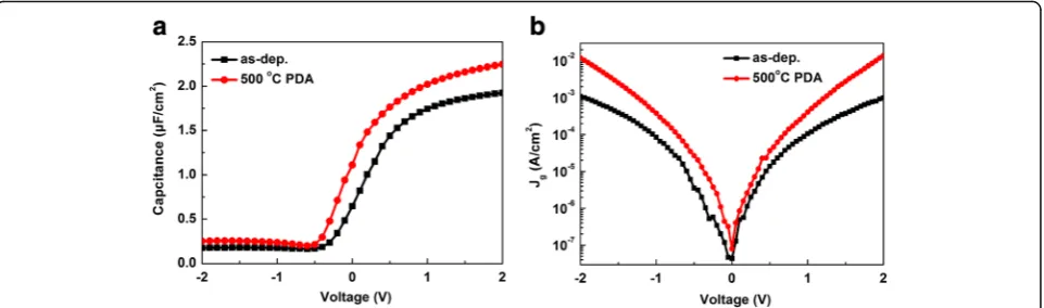
Figure 2a plots the high-frequency (1 MHz) C-V curves of HfO2/SiO2gate stacks on Ge before and after
PDA. It can be found that flat band voltage (Vfb) values
of HfO2/SiO2/Ge before and after PDA are 0.42 and
0.27 V, respectively. The calculated ideal Vfb value is
0.55 V. The slightly negative Vfb shift indicates positive
fixed charges, which may be induced by the oxygen va-cancies in the dielectrics [26, 27]. During the inert at-mosphere annealing process, more oxygen vacancies may be induced, resulting in a slightly negativeVfbshift.
It has been demonstrated in many reported literatures that the GeO2 degradation during the annealing will
cause the positive Vfb shift. The desorption process of
Ge-O is believed to generate additional negative charges [28, 29]. Therefore, it can also be concluded that GeO2
decomposition is suppressed by Ge-O-Si interlayer from
Vfb shift. The accumulation capacitance evidently
in-creases from the original 1.92 to 2.25μF/cm2after PDA. The corresponding capacitance equivalent thickness (CET) values of the MOS capacitors can be calculated from the accumulation capacitances of the C-V curves using ε0εrA/Cacc [30]. Therefore, a smaller CET of
1.53 nm is obtained after PDA compared to as-deposited sample of 1.80 nm. It can be ascribed to the fact that a denser and thinner high-k layer can be acquired after PDA process. Figure 2b shows the leakage current char-acteristics of HfO2/SiO2 films on Ge before and after
PDA. At the bias voltage ofVfb+ 1 V, the leakage current
density is 2.1 × 10⁻³A/cm2and 2.2 × 10⁻⁴A/cm2for the
[image:3.595.62.537.88.337.2]sample before and after PDA, respectively. The increased leakage current density after PDA can be also attributed to the decrease of the gate dielectrics thickness.
In order to examine the interface quality of HfO2/
SiO2/Ge quantitatively, the interface state density (Dit)
was determined by the conductance method [31]. Fig-ure 3 shows the distribution ofDit below Ecin the band
gap extracted by the conductance method at room temperature for Pt/HfO2/SiO2/Ge before and after 500 °
C PDA. The Dit can be roughly calculated from Dit=
2.5 × (Gp/w)max/Aq, where (Gp/w)maxis the peak value of
conductance-voltage characteristics, f(=w/2π) is the fre-quency, A is the electrode area, and q is the elemental charge. Therefore, Dit values of Pt/HfO2/SiO2/Ge
struc-tures without and with PDA are determined to be 4.05 × 10¹² eV−1 cm-2 and 5.37 × 10¹² eV−1 cm−2 at E-Ev=
0.38 eV, respectively. The lower Dit values of 2.03 ×
1012 cm−2eV−1and 2.67 × 1012cm−2eV-1near the bottom of conduction band are observed for the samples without and with PDA, respectively.
Figure 4 illustrates the leakage current density (Jg
)-CET relationship of Ge-based MOS capacitor with dif-ferent interfacial control layer [32, 33]. Compared to the S-passivated Ge without interlayer reported by our pre-vious work [34], the HfO2/SiO2/Ge in this work exhibits
much improved properties with smaller CET (1.53 vs 2.18 nm), leakage current density (2.1 × 10⁻³ vs 3.1 A/ cm2), and Dit (4.37 × 10¹² vs 8.61 × 10¹² eV−1 cm−2). It
implies that in situ PEALD-formed SiO2 is a wonderful
passivation layer for Ge. Moreover, compared to the ex situ-formed SiO2 interlayer by MOCVD [9], the sample
with in situ PEALD-formed SiO2interlayer in this work
shows better electrical performance with both smaller CET (1.53 vs 1.75 nm) and leakage current density (2.1 vs 3.9 mA/cm2). It can be ascribed to the fact that SiO2
de-posited by PEALD are more uniform than MOCVD espe-cially for ultrathin thickness.
The band alignment at HfO2/SiO2/Ge interface was
also determined by measuring the valence band offset
ΔEv(VBO) using XPS. The VBO values can be obtained
based on the assumption that the energy difference be-tween the core level and the valence band (VB) edge of the substrate remains constant with/without the depos-ition of dielectrics films [35]. Here, the Ge substrate was chosen as the reference to determine the VBO between gate dielectrics stack and Ge substrate. Figure 5a presents the VB spectra of the clean Ge substrate, as-deposited and annealed HfO2/SiO2/Ge stacks determined by linear
ex-trapolation method, respectively. The VB edge of the clean Ge substrate has been determined to be 0.10 eV. And, the VB edges of as-deposited and annealed HfO2/SiO2
sam-ples are found to be 2.55 and 2.79 eV, respectively. It can be noticed that there is a small tail in VB spectra for HfO2/SiO2/Ge stacks, which is corresponding to Ge
sub-strate signal [36]. The leading edge of this weak tail is measured to be 0.10 eV and the same as the VB edge of Ge substrate. Therefore, the VBOs at the interface of HfO2/SiO2/Ge with and without PDA are estimated to be
Fig. 3Distribution of Ditbelow Ecin the band gap at room temperature for Pt/HfO2/SiO2/Ge before and after 500 °C PDA
Fig. 2Electric characteristics of HfO2/SiO2gate stacks on Ge substrates before and after 500 °C PDA.aHigh-frequency (1 M Hz) C-V curves.b J-V curves
[image:4.595.59.540.88.230.2] [image:4.595.57.291.528.704.2]2.69 and 2.45 eV, respectively. The conduction-band offset
ΔEc (CBO) can be obtained by subtracting the VBO and
the bandgap of the substrate from the bandgap of HfO2:
ΔEc¼EgðHfO2Þ−Egð ÞGe −ΔEv;
where Eg(HfO2) and Eg(Ge) are the bandgap of HfO2
and Ge, respectively. The bandgaps of Ge and HfO2are
0.67 and 5.6 eV, respectively. Therefore, the CBO values at the interface of HfO2/SiO2/Ge with and without PDA
are estimated to be 2.24 and 2.48 eV, respectively. The CBO values are consistent with the previously reported data of 1.8–2.6 eV [37]. Figure 5b illustrates the corre-sponding band alignment of as-deposited and annealed HfO2/SiO2/Ge structures. Evidently, the HfO2/SiO2
high-k gate dielectric stacks on Ge exhibit large VBO
and CBO values with huge barrier heights to inhibit leakage current.
Conclusions
In summary, SiO2 interlayer was introduced into HfO2
gate dielectrics on n-Ge substrates successfully by in situ PEALD. We have investigated the interfacial, electrical properties, and band alignment of HfO2/SiO2/Ge MOS.
It has been demonstrated that Ge-O-Si interlayer and GeO2 layer is formed on Ge surface during the in situ
SiO2deposition. This Ge-O-Si interlayer shows fantastic
thermal stability during PDA without Hf-silicates forma-tion. Moreover, Ge-O-Si interlayer can also inhibit the GeO2degradation during annealing process. The HfO2/
SiO2/Ge sample after PDA exhibits a CET value of
1.53 nm with low leakage current density of 2.1 × 10⁻³ A/cm2at Vfb+ 1 V. The VBO values at the HfO2/SiO2/Ge
Fig. 4Leakage current density (Jg)-CET relationship for Ge-based MOS capacitors with different interfacial control layer
[image:5.595.60.540.88.299.2] [image:5.595.59.539.560.701.2]with and without PDA are determined to be 2.69 and 2.45 eV, and the CBO values to be 2.24 and 2.48 eV, re-spectively. Compared to the ex situ-formed SiO2interlayer
by MOCVD, the sample with in situ PEALD-formed SiO2
interlayer in this work shows improved electrical perform-ance, ascribed to the fact that SiO2deposited by PEALD
are more uniform than MOCVD. Therefore, PEALD is a much more powerful technology for ultrathin interfacial control layer deposition than MOCVD.
Acknowledgements
This project is supported by the Natural Science Foundation of China and Jiangsu Province (51571111 and BK2016230), a grant from the State Key Program for Basic Research of China (2015CB921203).
Authors’Contributions
YQC and BW carried out the sample fabrication and device measurements. YQC and BW did the data analysis and interpreted the results. ADL and DW participated in the discussion of results. YQC drafted the manuscript. ADL supervised the whole work and revised the manuscript. All authors critically read and commented on the manuscript. All authors read and approved the final manuscript.
Competing Interests
The authors declare that they have no competing interests.
Publisher’s Note
Springer Nature remains neutral with regard to jurisdictional claims in published maps and institutional affiliations.
Received: 16 March 2017 Accepted: 13 April 2017
References
1. Lee ML, Leitz CW, Cheng Z, Pitera AJ, Langdo T, Currie MT et al (2001) Strained Ge channel p-type metal-oxide-semiconductor field-effect transistors grown on Si1-xGex/Si virtual substrates. Appl Phys Lett 79(20): 3344–6
2. Chui CO, Ito F, Saraswat KC (2006) Nanoscale germanium MOS dielectrics-part I: Germanium oxynitrides. Electron Devices IEEE Trans 53(7):1501–8 3. Ye PD, Wilk GD, Yang B, Kwo J, Chu SNG, Nakahara S et al (2003) GaAs
metal-oxide-semiconductor field-effect transistor with nanometer-thin dielectric grown by atomic layer deposition. Appl Phys Lett 83(1):180–2 4. de Souza JP, Kiewra E, Sun Y, Callegari A, Sadana DK, Shahidi G et al (2008)
Inversion mode n-channel GaAs field effect transistor with high-k/metal gate. Appl Phys Lett 92(15):153508
5. Molle A, Spiga S, Andreozzi A, Fanciulli M, Brammertz G, Meuris M (2008) Structure and interface bonding of GeO2/Ge/In0.15Ga0.85As heterostructures. Appl Phys Lett 93(13):133504
6. Kamata Y (2008) High-k/Ge MOSFETs for future nanoelectronics. Mater Today 11(1-2):30–8
7. Caymax M, Van Elshocht S, Houssa M, Delabie A, Conard T, Meuris M et al (2006) HfO2as gate dielectric on Ge: Interfaces and deposition techniques. Mater Sci Eng B 135(3):256–60
8. Xie Q, Deng S, Schaekers M, Lin D, Caymax M, Delabie A et al (2012) Germanium surface passivation and atomic layer deposition of high-k dielectrics-a tutorial review on Ge-based MOS capacitors. Semicond Sci Technol 27(7):1528–30
9. Li XF, Liu XJ, Fu YY, Li AD, Zhang WQ, Li H et al (2012) Effect of annealing on interfacial and band alignment characteristics of HfO2/SiO2gate stacks on Ge substrates. J Vacuum Sci Technol B 30(1):010602
10. Taoka N, Harada M, Yamashita Y, Yamamoto T, Sugiyama N, Takagi S-i (2008) Effects of Si passivation on Ge metal-insulator-semiconductor interface properties and inversion-layer hole mobility. Appl Phys Lett 92(11):113511 11. Li XF, Liu XJ, Zhang WQ, Fu YY, Li AD, Li H, et al (2011) Comparison of the
interfacial and electrical properties of HfAlO films on Ge with S and GeO2 passivation. Appl Phys Lett 98(16):162903.
12. Zhang L, Li H, Guo Y, Tang K, Woicik J, Robertson J et al (2015) Selective passivation of GeO2/Ge interface defects in atomic layer deposited high-k MOS structures. ACS Appl Mater Interfaces 7(37):20499–506
13. Asahara R, Hideshima I, Oka H, Minoura Y, Ogawa S, Yoshigoe A et al (2015) Comprehensive study and design of scaled metal/high-k/Ge gate stacks with ultrathin aluminum oxide interlayers. Appl Phys Lett 106(23): 15–4
14. Xie Q, Musschoot J, Schaekers M, Caymax M, Delabie A, Qu XP et al (2010) Ultrathin GeOxNyinterlayer formed by in situ NH3plasma pretreatment for passivation of germanium metal-oxide-semiconductor devices. Appl Phys Lett 97(22):2902
15. Cao YQ, Chen J, Liu XJ, Li X, Cao ZY, Ma YJ et al (2015) HfO2/GeOxNy/ Ge gate stacks with sub-nanometer capacitance equivalent thickness and low interface trap density by in situ NH3plasma pretreatment. Appl Surf Sci 325:13–9
16. Li XF, Liu XJ, Cao YQ, Li AD, Li H, Wu D (2013) Improved interfacial and electrical properties of atomic layer deposition HfO2films on Ge with La2O3 passivation. Appl Surf Sci 264:783–6
17. Zimmermann C, Bethge O, Winkler K, Lutzer B, Bertagnolli E (2016) Improving the ALD-grown Y2O3/Ge interface quality by surface and annealing treatments. Appl Surf Sci 369:377–83
18. Matsubara H, Sasada T, Takenaka M, Takagi S (2008) Evidence of low interface trap density in GeO2/Ge metal-oxide-semiconductor structures fabricated by thermal oxidation. Appl Phys Lett 93(3):032104–3 19. Kita K, Lee CH, Nishimura T, Nagashio K, Toriumi A (2009) Control of
properties of GeO2films and Ge/GeO2interfaces by the suppression of GeO volatilization. ECS Trans 19(2):101–16
20. Kita K, Suzuki S, Nomura H, Takahashi T, Nishimura T, Toriumi A (2007) Dramatic improvement of GeO2/Ge MIS characteristics by suppression of GeO volatilization. Ecs Trans 11(4):111–22
21. Kita K, Suzuki S, Nomura H, Takahashi T, Nishimura T, Toriumi A (2008) Direct evidence of GeO volatilization from GeO2/Ge and impact of its suppression on GeO2/Ge metal-insulator-semiconductor characteristics. Jpn J Appl Phys 47(4):2349
22. Nakashima H, Iwamura Y, Sakamoto K, Wang D, Hirayama K, Yamamoto K et al (2011) Postmetallization annealing effect of TiN-gate Ge metal-oxide-semiconductor capacitor with ultrathin SiO2/GeO2bilayer passivation. Appl Phys Lett 98(25):252102
23. Yamamoto K, Ueno R, Yamanaka T, Hirayama K, Yang H, Wang D et al (2011) High-performance Ge metal-oxide-semiconductor field-effect transistors with a gate stack fabricated by ultrathin SiO2/GeO2bilayer passivation. Appl Phys Express 4(5):051301–3
24. Di Z, Zhang M, Liu W, Shen Q, Luo S, Song Z et al (2005) Interfacial and electrical characteristics of Al2O3gate dielectric on fully depleted SiGe on insulator. Appl Phys Lett 86(26):262102
25. Renault O, Samour D, Damlencourt JF, Blin D, Martin F, Marthon S et al (2002) HfO2/SiO2interface chemistry studied by synchrotron radiation x-ray photoelectron spectroscopy. Appl Phys Lett 81(19):3627–9
26. Deng S, Xie Q, Deduytsche D, Schaekers M, Lin D, Caymax M et al (2011) Effective reduction of fixed charge densities in germanium based metal-oxide-semiconductor devices. Appl Phys Lett 99(5):437
27. Choi C, Lee JC (2010) Scaling equivalent oxide thickness with flat band voltage (VFB) modulation using in situ Ti and Hf interposed in a metal/high-k gate stacmetal/high-k. J Appl Phys 108(6):197
28. Cheng CC, Chien CH, Luo GL, Yang CH, Kuo ML, Lin JH et al (2007) Study of thermal stability of HfOxNy/Ge capacitors using postdeposition annealing and NH3plasma pretreatment. Entrepreneurship Regional Dev 154(7):229–52
29. Bai W, Lu N, Kwong DL (2005) Si interlayer passivation on germanium MOS capacitors with high-κdielectric and metal gate. IEEE Electron Device Lett 26(6):378–80
30. Kraut E, Grant R, Waldrop J, Kowalczyk S (1980) Precise determination of the valence-band edge in x-ray photoemission spectra: application to measurement of semiconductor interface potentials. Phys Rev Lett 44(24):1620
31. Nicollian EH, Brews JR (1982) MOS (metal oxide semiconductor) physics and technology. Wiley, New York, Chapter 5
32. Gao J, He G, Fang Z, Lv J, Liu M, Sun Z (2016) Interface quality modulation, band alignment modification and optimization of electrical properties of HfGdO/Ge gate stacks by nitrogen incorporation. J Alloys Compd 695:2199–206
33. Cheng ZX, Liu L, Xu JP, Huang Y, Lai PT, Tang WM (2016) Impact of nitrogen incorporation on the interface between Ge and La2O3or Y2O3 gate dielectric: a study on the formation of germanate. IEEE Trans Electron Devices 63(12):4888–92
34. Li XF, Cao YQ, Li AD, Li H, Wu D (2012) HfO2/Al2O3/Ge gate stacks with small capacitance equivalent thickness and low interface state density. ECS Solid State Lett 1(2):N10–N2
35. Mi Y, Wang S, Chai J, Pan J, Huan A, Ning M et al (2006) Energy-band alignments at LaAlO3and Ge interfaces. Appl Phys Lett 89(20):2107 36. Dalapati GK, Oh HJ, Lee SJ, Sridhara A, Wong ASW, Chi D (2008)
Energy-band alignments of HfO2on p-GaAs substrates. Appl Phys Lett 92(4):042120 37. Seo KI, Mcintyre PC, Sun S, Lee DI, Pianetta P, Saraswat KC (2005) Chemical
states and electronic structure of a HfO2/Ge(001) interface. Appl Phys Lett 87(4):042902–3
Submit your manuscript to a
journal and benefi t from:
7Convenient online submission
7Rigorous peer review
7Immediate publication on acceptance
7Open access: articles freely available online
7High visibility within the fi eld
7Retaining the copyright to your article